ISSN(Online) : 2319-8753
I
nternational
J
ournal of
I
nnovative
R
esearch in
S
cience,
E
ngineering and
T
echnology
(An ISO 3297: 2007 Certified Organization)
Vol. 3, Issue 3, March 2014
Design and Implementation of FPGA Using
Error Tolerant Adder for Image Processing
Application
N.Nandhagopal 1, B.Senthilraja2
Associate Professor, Department of Electronics and Communicaton Engineering, SKP Engineering College Tiruvannamalai, Tamilnadu, India1
Assistant Professor, Department of Electronics and Communicaton Engineering, SKP Engineering College Tiruvannamalai, Tamilnadu, India2
ABSTRACT: In the era of low power, high performance digital systems are needed to boost up the technology revolution in nano-electronics. Realization of new digital logic is essential for making revolutionary changes in low power and high speed performance. In modern VLSI technology, the occurrence of all kinds of errors has become inevitable. By adopting an emerging concept in VLSI design and test, error tolerance (ET), a novel error-tolerant adder (ETA) is proposed. The ETA is able to ease the strict restriction on accuracy, and at the same time achieve tremendous improvements in both the power consumption and speed performance. A robust and efficient error-tolerant adder (ETA) is proposed in this project and it is compared with its conventional counterparts, with respect to power consumption and high speed. The proposed ETA is then applied for an image processing application and tested for its performance in terms of error tolerance. A novel type of adder, the error-tolerant adder, which trades certain amount of accuracy for significant power saving and performance improvement, is proposed. One example of such applications is in the image processing.
KEYWORDS: Error tolerant Adder, low-power and high speed circuit, VLSI, Image processing. I. INTRODUCTION
In conventional digital VLSI design, most digital data are processed and transmitted in a noisy channel. During this process, errors may occur anywhere in the processing chain. Error-tolerant concept cannot be adopted for all systems – In digital control systems, the correctness of the output signal is extremely important, and this denies the use of the error tolerant circuit. In modern VLSI technology, the occurrence of all kinds of errors has become inevitable. By adopting an emerging concept in VLSI design and test, error tolerance (ET), a novel error-tolerant adder (ETA) is proposed. The ETA is able to ease the strict restriction on accuracy, and at the same time achieve tremendous improvements in both the power consumption and speed performance.
A robust and efficient error-tolerant adder (ETA) is proposed in this project and it is compared with its conventional counterparts, with respect to power consumption and speed. The proposed ETA is then applied for a typical signal processing application (image processing and speech processing systems, the error-tolerant circuits may be applicable) and tested for its performance in terms of error tolerance.
Increasingly huge data sets and the need for instant response require the adder to be large and fast. The traditional ripple-carry adder (RCA) is therefore no longer suitable for large adders because of its low-speed performance. Many different types of fast adders, such as the carry-skip adder (CSK), carry-select adder (CSL) and carry-look-ahead adder (CLA) have been developed – But all of them suffer a trade-off between speed and power.ETA can attain great improvement in both the power consumption and speed performance.
ISSN(Online) : 2319-8753
I
nternational
J
ournal of
I
nnovative
R
esearch in
S
cience,
E
ngineering and
T
echnology
(An ISO 3297: 2007 Certified Organization)
Vol. 3, Issue 3, March 2014
image processing application. The first part has three separate blocks. Clock divider, Transmitting section and another one is receiving section. clock divider is work as an incoming clock frequency 20 MHZ is divided by a factor 1042and again divide by two to achieve 9600 baud is used for both transmission and reception of pc & FPGA. For that receiving section the received data from PC is 9600 baud rate. The received data is used for image processing application using low power high speed adder. Reception is done by accumulating one bit at a time than shifting left. Next, the transmitting blocks performing the reverse operation of receiving block. Each bit is separated from data output and shifted right to achieve serial transmission. This process is repeated eight times.
II.LOW POWER HIGH SPEED ERROR-TOLERANT ADDER
A. TERMINOLOGY
The ETA, the definitions of some commonly used terminologies are given as follows.
Overall error (OE): OE = | Rc – Re | Where Re is the result obtained by the adder, and Rc denotes the correct result.
Accuracy (ACC): The accuracy of an adder is used to indicate how “correct” the output of an adder is for a particular input.
Minimum acceptable accuracy (MAA):The accuracy of an acceptable output should be high enough to meet the requirement of the whole system.MAA is just that threshold value.
Acceptance probability (AP): Acceptance probability is the probability that the accuracy of an adder is higher than the minimum acceptable accuracy.
B. REASON FOR DELAY & POWER CONSUMPTION IN DIGITAL ARITHMETIC CIRCUITS
Conventional adder circuit, the delay is mainly attributed to the carry propagation chain along the critical path; from the least significant bit (LSB) to the most significant bit (MSB).Significant proportion of the power consumption of an adder is due to the glitches that are caused by the carry propagation. Therefore, if the carry propagation can be eliminated or curtailed, a great improvement in speed performance and power consumption can be achieved.
C. PROPOSED ERROR TOLERANT ADDER ADDITION IN ARITHMETIC
Step -1: We first split the input operands into two parts: an accurate part that includes several higher order bits and the inaccurate part that is made up of the remaining lower order bits. The length of each part need not necessary be equal. The addition process starts from the middle (Joining point of the two parts) toward the two opposite directions simultaneously. In the example of two 16-bit input operands, A=“1011001110011010” (45978) and B= “0110100100010011”(26899), are divided equally into 8 bits each for the accurate and inaccurate parts.
Step – 2: Addition Process for Accurate part
The addition of the higher order bits (accurate part) of the input operands is performed from right to left (LSB to MSB) and normal addition method is applied. This is to preserve its correctness since the higher order bits play a more important role than the lower order bits.
Step-3: Addition Process for In Accurate part
The lower order bits of the input operands (inaccurate part) require a special addition mechanism. No carry signal will be generated or taken in at any bit position to eliminate the carry propagation path. To minimize the overall error due to the elimination of the carry chain, a special strategy is adapted, and can be described as follow:
1) Check every bit position from left to right (MSB to LSB).
2) if both input bits are “0” or different, normal one-bit addition is performed and the operation proceeds to next bit position;
3) If both input bits are “1,” the checking process stopped and from this bit onward, all sum bits to the right are set to “1.
ISSN(Online) : 2319-8753
I
nternational
J
ournal of
I
nnovative
R
esearch in
S
cience,
E
ngineering and
T
echnology
(An ISO 3297: 2007 Certified Organization)
Vol. 3, Issue 3, March 2014
The block diagram of the ETA Figure.1.that adopts our proposed addition arithmetic is provided in Figure. This most straightforward structure consists of two parts: an accurate part and an inaccurate part. The accurate part is constructed using a conventional adder such as the RCA, CSK, CSL, or CLA. The carry-in of this adder is connected to ground. The inaccurate part constitutes two blocks: a carry-free addition block and a control block. The control block is used to generate the control signals, to determine the working mode of the carry-free addition block.
Figure.1: LOW POWER HIGH SPEED ERROR-TOLERANT ADDER
D. DESIGN OF 32-BIT LOW POWER HIGH SPEED ERROR TOLERANT ADDER
Fault tolerance (FT) is the ability of a system to continue correct operation of its tasks after the occurrence of hardware of software faults .
Defect tolerance (DT) the term refers to any circuit implementation that tolerates more defects than a non-defect-tolerant implementation. Recently the “undefined” term error-tolerance has appeared in several documents. In some cases, the term seems to refer to the fact that hardware has defects, and that one needs the ability to reconfigure a device so that only the “good” circuitry is used. This concept seems to be a merger of DT and reconfigurable FT ideas. We put forth the following new definition of error-tolerance. A circuit is error-tolerant (ET) with respect to an application or system, if (1) it contains defects that cause internal and may cause external errors, and (2) the system that incorporates this circuit produces acceptable results. Since an ET circuit may produce erroneous results, ET is different from FT and DT. The primary interest in ET is that it has the potential to significantly enhance the effective yield of a process.
As VLSI scaling continues along its traditional path, chips will have billions of devises and thousands of defects. Using only FT and DT techniques might not be sufficient to produce functionally perfect chips at affordable prices. The case is clearly made in the 2001 International Technology Roadmap for Semiconductors (ITRS). One challenge they discuss is error-tolerance. Clearly, some applications require correct computation, such as banking and the control of a nuclear power plant. Many others do not. One large domain where perfect functional operation is not required is in some multi-media and many DSP applications. One good example of an error tolerant system is a MPEG motion detection encoder that provides excellent performance in the presence of a large fraction of single stuck-at faults.
ISSN(Online) : 2319-8753
I
nternational
J
ournal of
I
nnovative
R
esearch in
S
cience,
E
ngineering and
T
echnology
(An ISO 3297: 2007 Certified Organization)
Vol. 3, Issue 3, March 2014
In our proposed 32-bit ETA, the inaccurate part has 20 bits as opposed to the 12 bits used in the accurate part. The overall delay is determined by the inaccurate part, and so the accurate part need not be a fast adder. The ripple-carry adder, which is the most power-saving
Conventional adder has been chosen for the accurate part of the circuit.
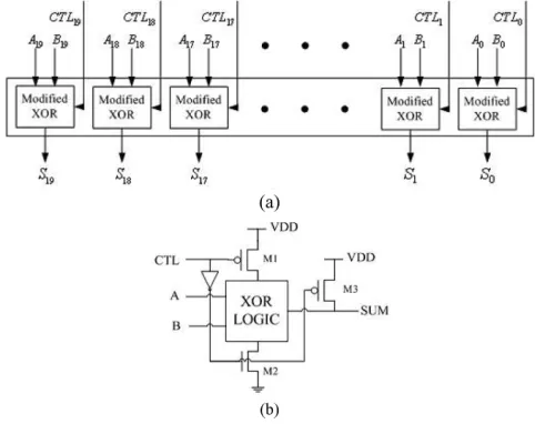
The inaccurate part is the most critical section in the proposed ETA as it determines the accuracy, speed performance, and power consumption of the adder. The inaccurate part consists of two blocks: the carry free addition block and the control block. The carry-free addition block is made up of 20 modified XOR gates, and each of which is used to generate a sum bit. The block diagram of the carry-free addition block and the schematic implementation of the modified XOR gate are presented in Fig. 2.
Fig. 2. Carry-free addition block. (a) Overall architecture and (b) schematic diagram of a modified XOR gate. In the modified XOR gate, three extra transistors, M1, M2, and M3, are added to a conventional XOR gate. CTL is the control signal coming from the control block of Fig.3 and is used to set the operational mode of the circuit. When CTL=0, M1 and M2 are turned on, while M3 is turned off, leaving the circuit to operate in the normal XOR mode. When CTL=1, M1 and M2 are both turned off, while M3 is turned on, connecting the output node to VDD, and hence setting the sum output to “1.”The function of the control block is to detect the first bit position when both input bits are “1,” and to set the control signal on this position
ISSN(Online) : 2319-8753
I
nternational
J
ournal of
I
nnovative
R
esearch in
S
cience,
E
ngineering and
T
echnology
(An ISO 3297: 2007 Certified Organization)
Vol. 3, Issue 3, March 2014
Fig. 3. Control block. (a) Overall architecture and (b) schematic implementations of CSGC.
Two types of CSGC, labelled as type I and II in Fig. 3(a), are designed, and the schematic implementations of these two types of CSGC are provided in Fig. 3(b). The control signal generated by the left most cell of each group is connected to the input of the leftmost cell in next group. The extra connections allow the propagated high control signal to “jump” from one group to another instead of passing through all the 20 cells. Hence, the worst case propagation path (shaded in gray in Fig. 3(a)) consists of only ten cells.
E. BLOCK DIAGRAM
Fig. 4 Block Diagram
ISSN(Online) : 2319-8753
I
nternational
J
ournal of
I
nnovative
R
esearch in
S
cience,
E
ngineering and
T
echnology
(An ISO 3297: 2007 Certified Organization)
Vol. 3, Issue 3, March 2014
F. SIMULATION RESULTS
To demonstrate the advantages of the proposed ETA, we simulated the ETA along with four types of conventional adders, i.e., the RCA, CSK, CSL, and CLA, using Xilinx. The input frequency was set to 20 MHz, and the simulation results are all tabulated in Table 1
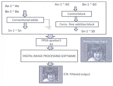
III. APPLICATION OF LOW POWER HIGH SPEED ERROR-TOLERANT ADDER IN IMAGE PROCESSING
In image processing and many other DSP applications, fast Fourier transformation (FFT) is a very important function. The computational process of FFT involves a large number of additions and multiplications. The input raw image is processed in spartan3 kit then the output of the image is obtained from PC. The input image error is filtered by the low power high speed adder and the output is obtained by clear format.
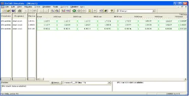
SIMULATION RESULTS:
ORCAD has been used to obtain the simulation results of Error Tolerant Adder (ETA).
Figure: 5 ETA simulation output
LOGIN FORM:
ISSN(Online) : 2319-8753
I
nternational
J
ournal of
I
nnovative
R
esearch in
S
cience,
E
ngineering and
T
echnology
(An ISO 3297: 2007 Certified Organization)
Vol. 3, Issue 3, March 2014
LOW POWER HIGH SPEED ETA AND ITS APPLICATION IN IMAGE PROCESSING:
Figure 7: Low Power High Speed ETA and its application in image processing
IV. CONCLUSION
In this paper, the concept of error tolerance is introduced in VLSI design. A novel type of adder, the error-tolerant adder, which trades certain amount of accuracy for significant power saving and performance improvement, is proposed. Extensive comparisons with conventional digital adders showed that the proposed ETA outperformed the conventional Adders in both power consumption and speed performance. The potential applications of the ETA fall mainly in areas where there is no strict requirement on accuracy or where super low power consumption and high-speed performance are more important than accuracy. One example of such applications is in the DSP application for portable devices such as cell phones and laptops.
REFERENCES
[1]. M. A. Breuer, “Intelligible test techniques to support error-tolerance,”in Proc. Asian Test Symp., Nov. 2004, pp. 386–393.
[2]. A. B. Melvin and Z. Haiyang, “Error-tolerance and multi-media,”in Proc. 2006 Int. Conf. Intell. Inf. Hiding and Multimedia SignalProcess., 2006, pp. 521–524.
[3]. M. A. Breuer, S. K. Gupta, and T. M. Mak, “Design and error-tolerance in the presence of massive numbers of defects,” IEEE Des. TestComput., vol. 24, no. 3, pp. 216–227, May-Jun. 2004.
[4]. Ning Zhu path, Wang Ling Goh, Weija Zhang, Kiat Seng Yeo, and Zhi Hui Kong,”Design of Low-Power High-Speed Truncation-Error-Tolerant Adder and Its Application in Digital Signal Processing”.
[5]. K. V. Palem, “Energy aware computing through probabilistic switching: A study of limits,” IEEE Trans. Comput., vol. 54, no. 9, pp.1123–1137, Sep. 2005
.[6].J. E. Stine, C. R. Babb, and V. B. Dave, “Constant addition utilizing flagged prefix structures,” in Proc. IEEE Int. Symp. Circuits and Systems (ISCAS), 2005.
[7].L.-D. Van and C.-C. Yang, “Generalized low-error area-efficient fixed width multipliers,” IEEE Trans. Circuits Syst. I, Reg. Papers, vol. 25,no. 8, pp. 1608–1619, Aug. 2005.
[8]V. C. Prasad, N. S. C. Babu, "Selection of test nodes for analog fault diagnosis in dictionary approach", IEEE Trans. Instrum. Meas., vol. 49, pp. 1289-1297, Dec. 2000.
[9]H. Chung, A. Ortega, "Analysis and testing for error tolerant motion estimation", Proc. Int'l Symp. on Defect and Fault Tolerance in VLSI Systems, pp. 514-522, 2005.