Low Power High Speed Dynamic Comparator
P
1
P
Swati Singh, P 2
P
Pankaj M. Gulhane,
P
1
P
M.Tech. Student, DIMAT
P
2
P
Asst. Professor, DIMAT [email protected]
Abstract – In high speed ADC, a comparator directly influence the overall performance of ADC. This paper describes the performance of latched comparator and also introduces a new technique that uses a differential amplifier in closed loop to
measure the offset of dynamic latch. The comparator circuit consists of a pre amplifier and a latch followed by a output buffer. The offset of preamplifier and latch is store and cancel by using a standard technique and gives output with high resolution. This comparator is designed in 0.18µm CMOS technology in LT-Spice and it can resolve the signals of 6.3Mv above and below the reference value. The clock used in 3 phase clock with a time period of 0.24µsec.
Index Terms: - Analog-to-Digital Converter, comparator, preamplifier, latch offset measurement, offset cancelation , latched comparator.
I. INTRODUCTION
Comparators are fundamental building block for
Analog-to-Digital converters and regulators. ADC’s
are used in many applications such as data storage
systems, fast serial links, high speed communication
and interfaces, which required for high resolution and
high speed of the order of GSPS.
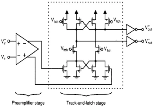
Latched Comparator
Architecture of modern high speed comparator
essentially consists of a preamplifier stage and a latch
stage. The preamplifier stager amplifies the input
signal to improve the comparator sensitivity and it also
isolates the input of the comparator from switching
noise coming from the positive feedback stage. The
second stage is latch stage which is used to determine
the larger input signal and thus need to have high gain.
Usually positive feedback is used to achieve high gain
and fast response.
fig. 1 Latched Comparator circuit
Offset Cancellation Techniques
Dynamic comparators are widely used in the high
speed ADCs due to its low power consumption and
fast speed. However, it is difficult to determine the
operation regions and bias conditions of transistors in a
dynamic comparator when mismatch exists. The
analog sampling capability inherent in CMOS
technologies provide a means whereby offsets can be
periodically sensed, stored , and then substracted from
the input.
Input Offset Storage
Fig. shows the Input Offset Storage (IOS) technique
applied to a comparator chain consisting of
pre-amplifier, offset storage capacitors (CRSR) and a latch. CRPR
is the parasitic capacitance at each node.
Fig. 2 Input Offset Storage
In the first phase unity gain loop is closed around the
preamplifier and the offset is stored on capacitor. In
the second phase input is applied and thus the total
residual offset is given by-
In the above equation GR0R is the gain of preamplifier
and VROSlR is the offset of latch and ∆q is the charge
injection from MOS switches. This offset can be
minimized by enlarging the gain of the pre-amplifier,
GR0R, thus VROSR is ultimately limited by the charge
injection of the switches, whose effect can only be
reduced by increasing CRSR.
Similarly in the output offset storage (OOS) technique
the offset is cancelled by shorting the preamplifier
inputs and storing the amplified offset on the ouput
coupling capacitors.
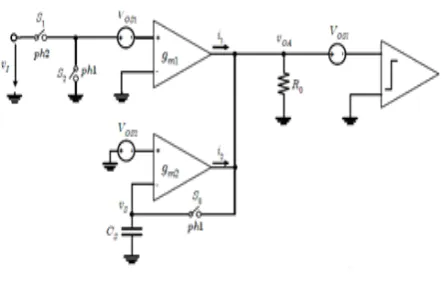
Offset reduction using Auxiliary Differential
Pairs-An another approach is to use an auxiliary differential
pair that isolates the signal path from the offset storage
capacitors, while performing offset cancellation.
Figure presents such an implementation. The auxiliary
differential pair, gm2, is connected to the output of the main differential pair, gm1. R0 is the load resistance.
Fig. 3 use of auxiliary differential pair
In the offset sampling phase, ph1, switches S2 and S3 are turned on, and a unity gain loop is closed around
gRm2R, charging CRSR. In normal operation S1 is on, and the auxiliary differential pair adds a DC current to the
output of the main amplifier, that (ideally) cancels its
offset voltage.
The total residual offset referred at input is:
Once again VROSlR appears divided by the gain of the
main amplifier, because this technique does not
compensate the offset of the latched comparator. A
large CRSRreduces the charge injection term, but affects
the output voltage settling speed during ph1.Thus the offset is reduced by the gain of auxiliary amplifier.
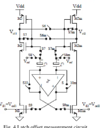
Offset cancellation technique for latch
Figure 4 shows the basic configuration of the dynamic
latch offset measurement technique which uses a
differential amplifier.
Fig. 4 Latch offset measurement circuit
This circuit has two modes of operation. The first is
the differential amplifier evaluation, and latch offset
measurement mode. During this mode of operation,
switches S6, S6m, S8, S8m, S10, and S10m are not
conducting. Switches S5, S5m, S7, S7m, S9, and S9m
are conducting. The amplifier is embedded in a closed
negative feedback loop. Intuitively, the loop works as
follows: If due to some device mismatch, Vol1 starts to fall and Vol2 starts to rise, the differential amplifier will apply a voltage difference of A2(Vol2 − Vol1) to the latch inputs in a sense that will drive the voltage
difference between the latch output nodes back close to
zero. The second operating mode of this circuit is the
latch regeneration and differential amplifier input
offset storage mode, where now we have S6, S6m, S8,
S8m, S10, and S10m conducting, while S5, S5m, S7,
S7m, S9, and S9m are not conducting. Therefore, the
latch positive feedback is activated.
Proposed Technique for Comparator design
The circuit designed is for the proposed technique
shown in Fig 5 The comparator consists of a
preamplifier, an auxiliary amplifier, a latch and a
differential pair for offset measurement of latch. Here
the capacitors are not in the signal path and hence the
speed as compared to that of the existing technique is
greater. The offset storage and cancellation is through
an auxiliary amplifier.
Fig. 5 Schematic of Proposed technique
In the proposed technique, the latch offset
measurement is done by the differential amplifier and
offset cancellation is done through auxiliary amplifier.
The offset cancellation is again done in two phases:
Offset storage phase and evaluation and cancellation
phase.
The comparator circuit uses 3 phase clocking. The
behaviour of the circuit during these phases is as
follows:
U
Phase1:
During this phase of clock, the switches S2a,b, S4a,b,
S5a,b, S7a,b and S9a,b conduct. In this phase
pre-amplifier offset voltages are amplified and stored on
Ca1 and Ca2 respectively. The latch offset
measurement process is activated and the latch inputs
g1 and g2 act like voltage sources with value VOSl1
and VOSl2 respectively.
U
Phase 2:
During this phase switches S1a,b, S8a,b and S10a,b
conduct while S2a,b, S4a,b, S7a,b and S9a,b are
opened. S5a,b still conduct. The inputs Vin and VR are
applied to the comparator. The latch offset
measurement loop is broken. The latch positive
feedback is still disabled. Offset Voltages of the latch
offset measurement amplifier are being stored on C1
and C2, so that they get cancelled during offset
measurement of the latch.
U
Phase 3:
During this phase only switches S4a,b, S5a,b and
S6a,b change their switching states, rest all switches
remain in their previous states. The latch positive
feedback is activated after the imbalance has been
applied to the latch inputs. The latch regenerates to
either one of its two final states.
Results of Implementation-
The whole circuitry is implemented in 0.18µm CMOS
technology in LT-Spice (level-8). In this design offset
of 10mv is kept between the two thresholds of the
input transistor.
Power Supply 3.3V
Gain of preamplifier 11
Load capacitance 0.1pf
Power 300µW
Clock period 0.24µsec
Resolution 6.3mv above and below
reference (1.65)
Area 3.6µmP
2
Table 1
Table 1 lists some performance parameters for the
comparator of Fig.5. The comparator can resolve
signals of 6.3mv above and 6.3mv below the reference
value (i.e. Resolution). The speed is greater
(0.24µsec).
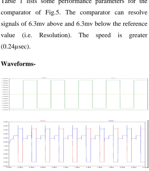
Waveforms-
Fig. 6 Input and Output waveforms for proposed technique
The waveforms shown in Fig.6 are the input and
output waves. The input waveform is a pulse with
voltage varying from 1.6437 Volts to 1.6563 Volts, i.e.
6.3mV above and below the reference value of 1.65
Volts. The output waveform is the output of the latch
corresponding to the input signal applied. The output
waveform has 3 parts corresponding to each phase.
The waveform in blue is the wave at one of the outputs
and that in red is at the other output (complementary to
the wave in blue). The output is 3.3 (VRddR) volts if the
input is above the reference and is 0 Volts (gnd) if the
input is below the reference.
Conclusion
A low-offset high-speed voltage comparator has been
designed in 0.18um technology. . The offset of the
latch is first measured with the help of a differential
amplifier and the stored and cancelled through an
auxiliary amplifier. The novel design has a
amplifier gain of 11 and it can resolve signals of
6.3mV above and below the reference value. The clock
used is a 3-phase clock with a time period of 0.24usec.
REFERENCES:
1. David A. Johns, Ken Martin – Analog integrated circuit design – John Wiley & Sons, 1997.
2. R. Jacob Baker – CMOS: Circuit design, layout and simulation – 2P
nd
P
ed., John Wiley & Sons, 2007.
3. Behzad Razavi, Beuce A.Wooley,”Design
Techniques for High Speed, High-Resolution
Comparators”,IEEE JOURNAL OF SOLID
STATE CIRCUIT. VOL. 27, NO. 12,
DECEMBER 1992.
4. Sunghyun Park, Michael P. Flynn,”A
regenerative Comparator structure with
Integrated Inductors”,IEEE Transaction on
Circuits and Systems- I VOL.-53, NO. 6,
AUGUEST 2006.
5. Ali Valaee, Mohammadi Maymandi-nejad and
Vakilabad BLVD Mashhad, “An Ultra
Low-Power Low- Voltage Track and latch
Comparator”, IEEE ICECS 2010.
6. Meena Panchor and R. S. GAMAD, “Low
Power High Speed CMOS Comparator design
using 0.18 µm Technology”, ISSN 0975-6450
VOL- 2 NO. 1 (2010) pp 71-77
7. Guo Yongheng , Cai Wei, Lu Tiejun,
Wang Zongmin, “ANovel 1GSPS Low
Offset Comparator for High Speed ADC”,
IEEE computer society 2009
8. Samad Sheikhaei, Shahriar Mirabbasi, and Andre Ivanov” A 0.35μm CMOS Comparator Circuit for High Speed ADC
Applications”,IEEE NSERC 2005
9. Khayrollah Hadidi and Gabor C. Temes,
“A High Resolution Low Offset and High
Speed Comparator”, IEEE 1992 CUSOM
INTEGRATED CIRCUITS
CONFERENCE
10. Benjamin J. McCarroll, CharlEs G. Sodini
Hea Seung Lee, ”A High Speed CMOS
Comparator for Use in an ADC”, IEEE
JOURNALS OF SOLID STATE
CIRCUITS VOL 23, NO 1, Feb1988
11. P. E. Allen, and D.R. Holberg “CMOS
Analog Circuit Design” Second addition
Oxford university 2007
12. R JACOB BAKER“CMOS Circuit design
and layout and simulation”, IEEE PRESS
second edition