N bit Concurrent SEU recognition and rectification for Hybrid NVSRAM Cell Nishma NJ1 ,Dr. Keshaveni N2
Dept. of Electronics and Communication KVGCE, Sullia, DK, India
Abstract—The main project confronted through Hybrid NVSRAM cell with soft error tolerance. The proposed NVSRAM cell comprises of a 6T SRAM core and a Resistive RAM (RRAM), made of a 1T and a Programmable Metallization Cell (PMC). The proposed cell has simultaneous mistake recognition called as concurrent error detection (CED) what's more, rectification (error correction) capacities.CED is proficient utilizing a dualrail checker, while it is refined (corrected) by using the restore operation; information from the non-volatile memory component is replicated back to the SRAM core. The dual rail checker uses two XOR doors each made of 2 inverters and 2 ambipolar transistors, henceforth, it has a hybrid nature. The reproduction results demonstrate that the proposed plan is exceptionally proficient as far as various figures of merits.
Keywords—Memory Cell, Programmable Metallization Cell (PMC), SEU, Detection, Correction, Emerging Technology
I. INTRODUCTION
Scaling of CMOS has been made conceivable by moved forward creation/fabricating and also designprocedures. So called developing innovations have been generally answered to supersede or supplement CMOS. Integration of significantly different emerging technologies with CMOS has gained attention, thus creating new possibilities for designing circuits and systems. This type of design style is commonly referred to as “hybrid”
[1], because it exploits different characteristics of emerging technologies.
One of the rising technologydriven standards in memory frameworks is spoken to by the so called non-volatile resistive RAM (RRAM) [2]. Distinctive nonvolatile SRAM (NVSRAM) cells have been proposed.The volatile information held in the SRAM core is supplanted with the information held in the non-volatile capacity when a restore operation on force up is performed. Non-unpredictable components in light of resistive switching, for example, memristor have been as of late proposed for NVSRAM execution[3]. Security limitations and additionally multi-setting configurability (i.e. the capacity to store and work under different arrangements of setup information) require non-volatile operation in programmable chips, for example, FPGAs. Consequently non-volatile components have been proposed as an expansion to SRAMs in FPGAs [4]. In spite of these advances, the solid operation at nanometricfeature sizes stays of noteworthy concern [5]. The measure of charge put away on a circuit node is getting to be littler because of the lower supply voltage and the littler node capacitance.This makes circuits more vulnerable to spurious voltage and charge varieties created by remotely impelled marvels, for example, cosmic ray neutrons and α-particles [6].
requiring 11 transistors (i.e. 11T) has been proposed in [4].
This paper proposes a PMC-based NVSRAM cell with a new plan for SEU resilience. It considers the node of slightest charge (i.e. the basic charge) for relieving a SEU by achieving both recognition and rectification. Reenactment results demonstrate that the proposed plan is extremely productive in wording of various figures of merit.
II. PROPOSED NVSRAM CELL In this segment, the operational standards of the proposed NVSRAM cell are exhibited. This NVSRAM cell comprises of two sections: an unpredictable (6T) SRAM core and a RRAM hardware (comprising of a 1T and a 1X, where X signifies the sort of resistive component). The proposed cell (7T1P; X=P as it uses a PMC as non-volatilestockpiling/storage component) is appeared in Fig. 1.
Fig1: NVSRAM Cell
In a NVSRAM cell, the non-volatile capacity node has a substantial charge, so it is to a great degree tolerant to a SEU; this suggests likewise that a NVSRAM cell has an innate repetition in put away information and the information put away in the non-volatile (resistive) component still holds right information if the SRAM cell is influenced by a SEU. As debasement of the information put away in the non-volatile component of a cell because of a SEU is exceptionally far-fetched (if not outlandish), the information put away in the RRAM is a dependable copy of the one put away in the SRAM core. Also, the resistive
component in a NVSRAM is typically set on an alternate plane in the chip format, in this way guaranteeing different surprises are exceptionally unrealistic to influence both variants of the same information and saving information autonomy in the capacity capacities.
In all cells, it has been demonstrated that the non-unpredictable capacity node has a charge request of greatness bigger than the basic charge, in this manner making the information put away in the RRAM exceptionally solid. The use of this element however requires altering existing operations, (for example, read and write) and in addition presenting new ones, (for example, restore).
1. Write (Store): the information is writed to both the SRAM core and the PMC. 2. Read: the information is perused from
the SRAM core dependent upon no event of a SEU.
3. Restore: if a SEU happens, Concurrent Error Detection (CED) is utilized and this operation is evoked, such that the information put away in the PMC is exchanged to the SRAM core for redress.
4. Instant On: the information put away in the SRAM core is volatile, i.e. it is lost when there is no force supply. Once the supply voltage is again made accessible, the instant on operation is begun and the information put away in the PMC is exchanged additionally to the SRAM core.
Store operation
Amid the store (write) operation, information is writed in both the PMC and the SRAM core. The voltage at node EN is at GND, while the voltage at node ENB is at VDD. Transistor M8 and the transmission gateway (T1) are OFF.
Write "0" Operation
while the estimation of the PMC resistance must be ROFF (high resistance). The voltages at BL and BLB are at GND and VDD separately. The memory cell is chosen by setting the voltage at WL to VDD. The voltage at D is at GND. For the write operation of a PMC, the changing rate of the resistance of the PMC is identified with the voltage distinction crosswise over it; transistor M7 is turned ON by expanding the supply voltage and the voltage at Ctrl1 to Vdh amid the write operation; so the PMC is writed with the information relating to the voltages at D and Ctrl2. As the voltage at node D is at GND and the voltage at Ctrl2 is at Vdh, then a negative voltage is dropped over the PMC and its resistance is set to the OFF state (high resistance).
Write "1" Operation
For this situation, the voltage at node D must be at VDD while the PMC resistance must be put in the ON state (low resistance). In this way, the voltage at WL must be at VDD for selecting the memory cell, while the voltages at BL and BLB are at VDD and GND separately. The information put away in the SRAM (voltage at D) is at state '1'; both the PMC and the SRAM are writed in the meantime, so the supply voltage of the phone is Vdh amid the write operation. M7 must be ON to produce the voltage contrast over the PMC. Along these lines, the voltage at Ctrl1 is Vdh, while the voltage at Ctrl2 is at GND. A voltage contrast over the PMC exists and the write "1" operation is executed.
Restore operation
The restore operation exchanges (duplicates) the information put away in the PMC to the SRAM cell, i.e. at node D. The information put away in the PMC is perused by setting the voltages at Ctrl1 and Ctrl2 to GND and VDD individually. In the event that a "0" ('1') is put away in the PMC, the voltage at DP is at GND (VDD).For the restore operation, VWL is set at VDD, while the voltages at BL and BLB are shifted relying upon the put away information, i.e. for a "0" ('1') in the PMC, the voltages at BL
and BLB are given by GND and (VDD and GND) individually and the voltage at D is at GND (VDD).During the restore operation, the voltages at nodes EN and ENB are at GND and VDD separately; transistor M8 and the transmission door (T1) are OFF.
Instant On Operation
Amid the instant on operation, the voltages at EN and ENB are at GND and VDD separately. Instant on operation is begun by setting the voltages at Ctrl1 and Ctrl2 to VDD while the voltages at lines BL, BLB and WL are at GND; thus, M7 is turned ON, while the voltage at D fluctuates relying upon the estimation of the PMC resistance. Because of the high estimation of the PMC resistance in state '0', an instability may exist because of a releasing node in the middle of D and DN.
In any case, the little estimations of the ON state resistance of M1 and M7 (contrasted with the high resistance of the PMC) result in a low voltage at node D. This at long last turns OFF M3, accordingly keeping the release of node DN; thus, the voltage at D is at 0V. On the off chance that a "1" is put away in the PMC (with a low estimation of resistance), the voltage at D is at VDD while the voltage at DN is released through M3. Therefore, the data in the PMC is correctly restored to D.
III. REVIEW
Programmable Metallization Cell (PMC)
The Programmable Metallization Cell (PMC) otherwise called the Conducting Bridge Random Access Memory (CBRAM) is a resistive exchanging non-volatile component in view of the relocation of metallic particles through a strong electrolyte and the ensuing development and disintegration of a metallic conductive fiber (CF) interfacing the two terminals.
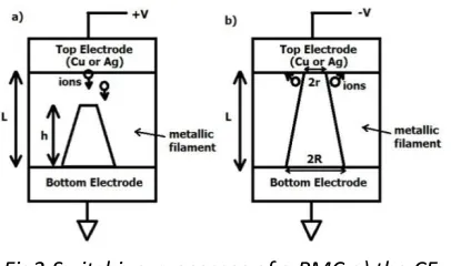
the CF vertically develops until it achieves the top anode, at which time the set procedure happens. Taking after the set process, the CF becomes horizontally and its measurement keeps on expanding, on the grounds that more metal particles are available around it.
Fig2:Switching processes of a PMC a) the CF vertically grows prior to set process, b) the CF
laterally dissolves prior to reset process
For the reset process, when a negative voltage predisposition happens over the PMC, the CF tends to along the side break up, in light of the fact that the upgraded sidelong electric field is at the highest point of the CF. The reset is finished when the width of the conductive fiber contracts down to zero at the top terminal. After the reset, the CF vertically breaks up and its stature continues diminishing. In this way, the exchanging procedure of a PMC has a move point that happens at whatever point the tip of the CF touches or isolates from the top anode. The resistance of a PMC is reliant on the CF height (h) and the CF range (r) for finding the ON and OFF-state resistance (Ron and Roff). The OFF state happens when the tip of the conductive fiber is isolated from the top terminal; for this situation, h is not exactly the film thickness of the strong electrolyte or the height of the PMC (L). When h is found, the OFF-state resistance (Roff) is given by the aggregate of two resistors in arrangement
Roff = (ρonh + ρoff(L - h))/A
The ON-state resistance of a PMC (Ron) happens when the tip of the CF touches the top cathode; the resistance quality depends on the
CF span (r). As the state of the conductive fiber is cone shaped, then the cell resistance of a PMC in the ON-state is as per the following
Ron = ρonL/(πrR) Ambipolar transistor
Not the same as a conventional (unipolar silicon CMOS) gadget whose conduct (either p-sort or n-sort) is resolved at creation, ambipolar gadgets can be worked in an exchanged mode (from p-sort to n-sort, or the other way around) by changing the gateway predisposition. Ambipolar conduction is portrayed by the superposition of electron and gap streams; this conduct has been tentatively reported in various rising innovations, for example, carbon nanotubes, graphene, silicon nanowires and natural single precious stones.
An ambipolar transistor can be utilized to control the bearing of the current taking into account the voltage at the alleged extremity door. A 4-terminals ambipolar transistor (Double Gate MOSFET, or DG-FET) is used in this paper. The second door (alluded to as the Polarity Gate, PG) controls its extremity, i.e. at the point when PG is set to logic '0', the ambipolar transistor carries on like a NMOS; when PG is set to logic '1', it acts like a PMOS
Fig 3 Ambipolar transistor, a) Symbol, b) Characteristics
Fig4: Model of ambipolar transistor
The conduct of the ambipolar transistor depends on the voltage at its extremity door. On the off chance that the voltage at node PG is GND, switch Sw1 is ON while Sw2 is OFF; the ambipolar transistor carries on as a NMOS. Be that as it may if the voltage at the extremity door is VDD, switches Sw1 and Sw2 are OFF and ON individually.
Soft Error (SE) and model
There is a broad specialized writing on SE-tolerant configuration for recollections. In a memory circuit, the transient voltage change that is created by a substantial particle strike, may straightforwardly prompt a Single Event Upset (SEU) as a state change of the memory cell. A SEU is said to happen when the gathered vitality Q at a specific node is more noteworthy than the basic charge, Qcrit, i.e. Qcrit is the base charge that should be kept at the touchy node of a capacity cell to flip (change) the put away piece (information). For the most part for a 6T SRAM core, Qcrit is found at one of the capacity nodes, i.e. DN or D.
Diverse solidifying approaches have been proposed to conquer a SEU. An illustration of a solidifying approach in memory outline is ordinarily known as DICE and uses double the quantity of transistors of a standard stockpiling cell (i.e. 12T versus 6T). The upside of this outline is that it doesn't require an expansion in the extent of the transistors or the capacitance of a few nodes. In the DICE cell, the single node that is influenced by a TF can be driven back to its past state by alternate transistors. An alternate solidified memory plan requiring 11 transistors (i.e. 11T) has been proposed in; the single node influenced by a TF can be driven back by utilizing novel get to and invigorating
circuits. Hypothetically, these two volatile plans are safe to any measure of charge gathered at any single node. Be that as it may they cause in noteworthy overhead as far as transistors added to the 6T SRAM core.
CED by dual-rail checker
Simultaneous mistake identification (CED) is used for enduring the event of a SEU. The CED circuit comprises of a double rail checker. The proposed configuration is cross breed in nature, since it has a further oddity in the circuit, in particular the utilization of ambipolar transistors in the XOR doors for the double rail checker.
Proposed XOR gateway
A CMOS XOR gateway requires no less than 8 transistors, while two more inverters are expected to create the converse information logic. In this way, the aggregate number of transistors is expanded to 12. Ambipolar transistors are utilized in this paper to diminish the quantity of transistors in a XOR gateway taking into account their attributes to act as either NMOS or PMOS. The diminishment in the quantity of transistors likewise enhances the force scattering.
Fig5:Proposed XOR gate
Double rail checker
the CED highlight. The double rail checker is associated with the proposed NVSRAM cell; for CED, M7 is killed, while the voltage at Ctrl2 is at VDD, the voltages at the three nodes are given as inputs to the two XOR gateways.
Fig6:Dual-rail checker for CED
Fig7:Ambipolar-based dual-rail checker
The yields of the double rail checker likewise guarantee that a solitary flaw happening in the proposed memory cell will be recognized as creating an invalid code at the yield, i.e. this circuit is self-checking as well. The restore operation in this way is required when VER1 = VDD and VER2 = 0. As portrayed already, the restore operation allows the information put away in the PMC to be writed back in the SRAM core, along these lines revising the SEU.
The ambipolar-based double rail checker that uses the proposed XOR gateways. Node DP is embedded at node IN1 of both the proposed XOR doors while nodes D and DN are associated with node IN2 of XOR1 and XOR2 individually.
IV. SIMULATION RESULTS
In this section, the proposed NVSRAM cell is evaluated by simulation. HSPICE is utilized as simulation tool, while the model of is
employed for simulating the PMC.
Delay, power dissipation, and PDP for write, read, and Restore operations of the proposed PMC-based NVSRAM cell.
Input voltage Output voltage Status Vd Vdn Vdp Ver1 Ver2
0 Vdd 0 0 Vdd No SEU
0 Vdd Vdd Vdd 0 SEU
Vdd 0 0 Vdd 0 SEU
Vdd 0 Vdd 0 Vdd No SEU
Fig9: CNFET results representing the voltages and current characteristics
Fig10: input voltage(vin) representation of 6T SRAM Cell
Fig11: vin1 & vin2 representation of 6T SRAM Cell
Fig12: output q representation of 6T SRAM Cell
Fig13: output qb representation of 6T SRAM Cell
V. CONCLUSION
This paper has introduced a novel way to deal with concurrent error detection and correction of a SEU in another memory cell. The proposed memory cell is hybrid in nature. Unique in relation to other SEU tolerant cells, the proposed memory cell is non-volatile and uses a double rail checker for simultaneous error recognition and the supposed restore operation for redress. The operational standards of the proposed NVSRAM have been examined and broad simulation results have been displayed for the greater part of its operations. Without a SEU, the proposed cell has faster read and write times contrasted and outlines utilizing hardening. The usage of a PMC results in a huge resistive reach, low equipment overhead, quick switching, however to the detriment of the necessity of higher voltage values for the store operation and higher PD and PDP esteem. This necessity recommends that the proposed cell is most appropriate for memories requiring non-volatile operation withfrequent read operations.
VI. REFERENCES
*1+ P. Junsangsri and F. Lombardi ”Design of a Hybrid Memory Cell UsingMemristance and Ambipolarity,” IEEE Transactions onNanotechnology, vol. 12, no. 1, pp. 71-80, 2013
*2+ H. Akinaga, H. Shima, “Resistive Random Access Memory (ReRAM) Based on Metal Oxides,” Proc. of the IEEE, pp. 2237-2251, 2010 [3] M. F. Chang, C. H. Chuang, M. P. Chen, L.-F. Chen, H. Yamauchi, P.-F. Chiu, S.-S. Sheu, “Endurance-Aware Circuit Designs of Nonvolatile Logic and Nonvolatile SRAM Using Resistive Memory (Memristor) Device”, 2012
17th Asia and South Pacific Design
AutomationConference (ASP-DAC), pp. 329-334,
2012
[4] X. Xue, W. Jian, Y. Xie, Q. Dong, R. Yuan, Y. Lin, “Novel RRAM Programming Technology for Instant-on and High-security FPGAs,” 2011 IEEE
9th International Conference on ASIC (ASICON),
pp. 291- 294, 2011
*5+ S. Lin, Y.B. Kim and F. Lombardi, “Soft-Error Hardening Designs of Nanoscale CMOS Latches,” Proc. IEEE VTS 2009, pp. 41 - 46, 2009 *6+ P.E. Dodd and L.W. Massengill, “Basic Mechanisms and Modeling of Single-Event Upset in Digital Microelectronics,” IEEE Transactions onNuclear Science, pp. 583 - 602, June 2003
*7+ T. Calin, M. Nicolaidis, R. Velazco, “Upset Hardened Memory Design for Submicron CMOS Technology,” IEEE Transactions on NuclearScience, Volume 43, Issue 6, Part 1, pp. 2874 - 2878, Dec. 1996
[8] M. H. B. Jamaa, K. Mohanram, G. D. Micheli "An Efficient Gate Library for Ambipolar CNTFET Logic" IEEE Trans. Computer-AidedDesign of Integrated Circuits and Systems, Vol. 30, No.2, Feb 2011
[9] P. Junsangsri, J. Han and F. Lombardi, ”Macro modeling a Phase Charge Memory (PCM) Cell by HSPICE,” Proc. IEEE/ACM Int.
Symposium onNanoarchitectures, pp. 77-84,
Amsterdam, July 2012.
[10] R. J. Baker "CMOS Circuit Design, Layout, and Simulation" Wiley- IEEE Press, Revised 2nd Edition, 2011