A Novel Omnidirectional Triangular Patch Antenna Array Using
Dolph-Chebyshev Current Distribution for C-Band Applications
Bhupendra Bhadoria and Sumit Kumar*
Abstract—In this paper the design and implementation of a patch antenna array using Dolph-Chebyshev current distribution operating in C-Band is demonstrated. The proposed novel omnidirectional triangular patch antenna array is a nonuniform array type with equal or uniform spacing between the antenna elements, but having the nonuniform amplitude excitation with Dolph-Chebyshev current distribution. Dolph-Chebyshev amplitude excitation suppresses the side lobes as well as the designed antenna works like an omnidirectional antenna. The proposed antenna array has a gain of 0.52 dB and return loss of −35.0649 dB which works as an omnidirectional antenna. This proposed antenna is suitable for C-band applications such as Wi-Fi devices, cordless phones, and keyless entry systems.
1. INTRODUCTION
In today’s wireless world, antennas have become the most important part of communication, in which microstrip patch antennas are being widely used due to their popularity. They have a thin profile, easy fabrication, shape flexibility unlike a slot antenna and dipole antenna, and can handle dual-frequency operation [1]. In the modern world where internet is needed mostly everywhere, more and more gadgets are made using microstrip patch antennas. Microstrip patch antennas are versatile and can be used for omnidirectional coverage, pencil beams and fan beams. They offer the decision of choosing linear polarization or circular polarization. Microstrip patch antennas are further combined to design antenna arrays which increase gain. An antenna array can be defined as a set of multiple single antennas and works as a single antenna to improve the gain. The larger the number of individual antenna elements is, the more the gain will be, and the narrower beam is achieved [2]. In linear antenna array, a uniform antenna array has uniform inter-element spacing as well as uniform current distribution to all antenna elements whereas a nonuniform antenna array has uniform inter-element spacing but nonuniform current distribution to all antenna elements. Binomial and Dolph-Chebyshev arrays are the different types of nonuniform antenna arrays. Binomial array has less directivity and lower number of side lobes, while Dolph-Chebyshev has good directivity as well as fewer side lobes [3–5]. Dolph-Chebyshev method is based on Chebyshev polynomial approximation for the pattern of the array. Now to distribute the output signal to the radiating antenna elements we need feed network. The effects of feed network are also very important in a high gain microstrip antenna array. There are different types of feeding techniques to improve the gain as well as directivity such as series, corporate and series-corporate, among which series-corporate feed has a higher directive gain than series and corporate feeding technique [6]. Now for an omnidirectional antenna we need to suppress side lobes. Side lobes represent unwanted radiation in undesired direction which results in wastage of energy and can cause interference to other equipments. One of the techniques for reducing the side lobes is by decreasing the distance between the
Received 14 May 2018, Accepted 23 July 2018, Scheduled 30 July 2018
* Corresponding author: Sumit Kumar ([email protected]).
two input ports while increasing the internal flares, which delays the occurrence of side lobes and keeping the return loss intact, i.e., below −10 dB [7]. The authors [8] employed CSRR (Complementary Split Ring Resonator) which creates the interferometer pattern to reduce side lobes. The parasitic patches can also be used for reducing side lobes [9]. The authors in [10] have designed an omnidirectional antenna which has low side lobes. The authors in [11] have used a cylindrical patch for omnidirectional characteristics. Use of triangular antenna [12, 13] elements in an array leads to the reduction of side lobe level, i.e., side lobe suppression. Also triangular antenna elements have smaller dimensions than a rectangular structure, so it is widely used in the applications where compact antenna is required or by using evolutionary algorithms such as Firefly algorithm, self adaptive differential evolution method and biogeography based optimization method [14]. The authors in [15] have fed a patch antenna array with corporate feed with appropriate amplitude tapers. Each antenna element is fed with individual separate feedline for low side lobes. In this paper, a triangular nonuniform antenna array is used with Dolph-Chebyshev amplitude excitation with corporate feed and is applied to uniform spaced triangular patch antenna elements. The designed antenna array operates in C-band [16], i.e., 4 GHz–8 GHz. Amplitude excitations to all the patches are different according to Dolph-Chebyshev polynomials so as to reduce the side lobes. The impedances to top patches, bottom patches and middle patch are different. The orientation of the paper is such that in the second section the design of antenna element is discussed such as length and width of antenna element as well as substrate used. In the third section, the design of the antenna array is discussed. In the fourth section, simulated and measured results and comparison between them are presented. The last section of the paper concludes the proposed work.
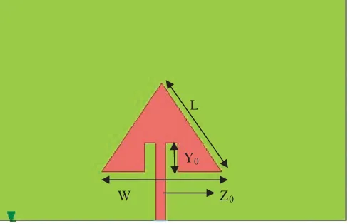
2. THE ANTENNA ELEMENT
The proposed triangular patch is shown in Figure 1. The patch is designed on an FR4 EPOXY dielectric substrate with relative permittivity of (γr) 4.4 and loss tangent (δ) of 0.02 with thickness of 1.6 mm. The length (L) and width (W) of the patch are 14.9 and 16.8 mm, respectively. The slot length for inset feed is 4 mm while the width is 2.9 mm.
L
W
Y0
Z0
Figure 1. Single C-band microstrip patch.
The length and width of the patch antenna calculated using Equations (1), (2) and (3) are shown in Table 1.
L = c
2fo√γ eff
−0.824h
⎛ ⎜ ⎜ ⎝
(γeff + 0.3)
W
h + 0.264
(γeff −0.258)
W
h + 0.8
⎞ ⎟ ⎟
⎠ (1)
W = c
2fo
γr+1
2
γeff =
(γr) + 1
2 +
(γr)−1 2 ⎡ ⎢ ⎢ ⎢ ⎢ ⎣ 1
1 + 12
h W ⎤ ⎥ ⎥ ⎥ ⎥ ⎦ (3)
whereL andW are the length and width of the patch antenna, and the substrate relative permittivity and thickness are γr = 4.4 and h = 1.6 mm, respectively. The substrate relative permittivity and thickness are γr= 4.4 and h= 1.6 mm, respectively.
Table 1. Dimensions of the antenna element.
Parameter Dimension (mm)
Patch Length, L 14.9
Patch Width,W 16.8
Antenna Substrate Thickness,ta 1.6
Slot Length, Y0 4
Slot Width, Z0 2.9
3. THE PROPOSED TRIANGULAR PATCH ANTENNA ARRAY
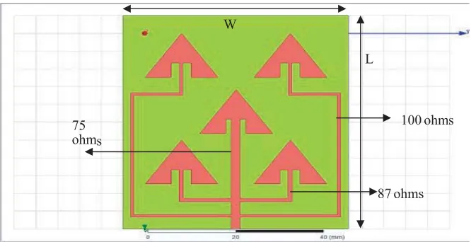
The proposed patch antenna array is shown in Figure 2. This patch array consists of 5 triangular microstrip patches and fed with nonuniform amplitude excitation with corporate feeding to reduce the side lobe level. It is designed on an FR4 EPOXY dielectric substrate with relative permittivity of (γr) 4.4, loss tangent (δ) of 0.02 and thickness of 1.6 mm. Dolph-Chebyshev amplitude excitation is applied to the patches. The bottom two patches have different feeding lines from top two and middle patches because we are using Dolph-Chebyshev amplitude excitation. The advantage of nonuniform array over uniform array is that it has low level side lobes. Binomial and Dolph-Chebyshev arrays are the different types of nonuniform antenna arrays, among which binomial array gives low level side lobes, and if the spacing between antenna elements is λ/2, it gives no side lobes with less gain and directivity, whereas Dolph-Chebyshev array has both good gain and directivity as well as good level of side lobe suppression. The microstrip patch antenna is designed to resonate in C-band, i.e., 4 GHz to 8 GHz. The length (L) and width (W) of the substrate are 60 mm and 51.8 mm, respectively. The impedance to top two patches
100 ohms 87 ohms 75 ohms L W
is 100 ohms, impedance to bottom two patches 87 ohms, and impedance to the middle patch 75 ohms. They are arranged in such a way that the resultant radiation pattern has the least side lobes. If we use an even array, i.e., even number of antenna elements, then there is no antenna element at the origin. On the other hand, if we use an odd array, an antenna element is present at the origin which is employed in our proposed antenna array.
4. SIMULATED AND EXPERIMENTAL RESULTS
The proposed antenna array is simulated on HFSS (High frequency Structure Simulator), and the results of designed antenna are verified on Vector Network Analyzer. Figure 3 shows that the designed antenna
Figure 3. Simulated return loss of antenna element.
Figure 5. Simulated return loss.
element resonates at 4.11 GHz and 5.68 GHz frequencies with return losses of−15.16 dB and−11.59 dB, respectively, which is below−10 dB in line with antenna design requirements.
Figure 4 shows the current distribution of the patches and is different due to the difference in the feed line width. In uniform power distribution, the impedance to all the transmitting feed lines is same, whereas for Dolph-Chebyshev impedance to each transmitting feed line is different with a different width to the feed lines which can be seen in Figure 4.
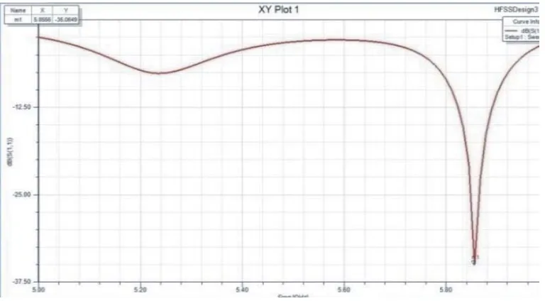
Figure 5 shows the simulated return loss or S11 parameter for the antenna array. The antenna
array resonates at the frequency 5.8556 GHz and has the return loss of −35.0649 dB which is below
−10 dB. The working bandwidth is 90 MHz and ranges from 5.811 to 5.9 GHz.
Figure 6 shows the 3-D radiation pattern of the proposed antenna array which shows that there are minimized back lobe, least side lobes and a maximum gain of−3 dB, and is almost similar to doughnut shape. It can be more optimized by increasing the substrate size, such that substrate is lambda/4 greater than the patch.
Figure 7 shows the two directional radiation patterns in E-plane and H-plane at the resonating frequency of 5.85 GHz and shows good omnidirectional radiation characteristics in horizontal plane.
Figure 7. E-plane andH-plane radiation pattern.
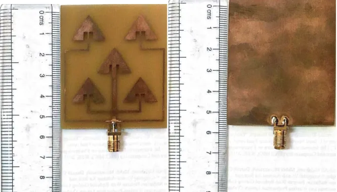
Figure 8 shows the prototype of the designed antenna. A patch antenna array is realized by deploying it on an FR4 EPOXY substrate with relative permittivity of 4.4 and height of 1.6 mm. The measured results of return loss, bandwidth, Smith chart and experimental setup are plotted in Figures 9–12, respectively.
Figure 8. Prototype of realized antenna array.
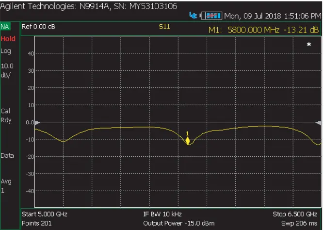
Figure 9 shows the measured result of return loss. It can be seen that the realized patch antenna array resonates at frequency 5.85 GHz with −13.21 dB return loss compared to a simulated return loss of −35.0649 dB and resonating at frequency 5.85 GHz.
Smith chart of the realized prototype of the antenna array is shown in Figure 10. It shows the impedance of 38.57 Ω at 5.85 GHz frequency.
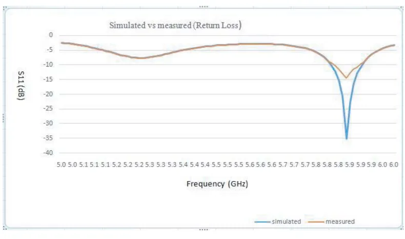
Figure 11 shows the comparison between the simulated and measured return losses which are
Figure 9. Measured return loss.
Figure 10. Smith Chart of realized prototype.
Table 2 shows the difference between the simulated and measured parameters such as frequency, return loss, bandwidth, and impedance of the patch antenna array. Measured results slightly differ from but show good agreement with the simulated results.
Table 2. Parametric analysis of simulated and measured results.
Parameters Simulated Measured
Frequency 5.85 GHz 5.85 GHz
Return Loss −35.0649 dB −13.21 dB
Bandwidth 90 MHz 80 MHz
Figure 11. Return loss (simulated vs measured).
Fabricated antenna array
VNA (Vector network analyzer)
Figure 12. Experimental setup.
Table 3. Comparison of antenna arrays.
Designed Antenna Size S11 (dB) VSWR
Antenna 1 [17] 42 mm (Each patch)∗4 −16.3353 1.4 (approx)
Antenna 2 [18] 74.4 mm×74.4 mm −16 1.42
Antenna 3 [19] 8 cm×9 cm −20.519 1.20
Antenna 4 [20] 70 mm×140 mm −27 1.09
Antenna 5 [21] 60 mm×60 mm −27 1.09
Figure 13. Cross-polarization.
Figure 12 shows the experimental setup which shows the realized prototype connected to vector network analyzer to measure the desired results.
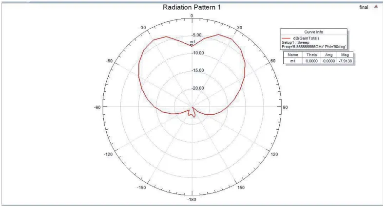
We have simulated cross polarization, shown in Figure 13. We found that cross polarization magnitude is−7.9 dB.
Table 3 shows the comparison of our proposed antenna array with different antenna array designs in the same frequency range, which clearly shows that the proposed antenna array has the highest S11
and lowest VSWR with a compact size among all antenna arrays in the same frequency range.
5. CONCLUSION
A C-band omnidirectional triangular patch antenna array is designed, investigated and experimentally validated. The antenna array gives return loss of−35.0649 dB at 5.85 GHz frequency simulated in HFSS, and realized prototype of antenna array has return loss of −13.21 dB at 5.85 GHz frequency which is in line with the simulated results. Both measured and experimental results show that the triangular patch antenna array can be designed as an omnidirectional antenna, and therefore, the triangular patch antenna array is a cheaper solution for omnidirectional antenna. The proposed antenna array with Dolph-Chebyshev current distribution shows good omnidirectional radiation characteristics with least side lobes. The proposed antenna array can be used for Wi-Fi devices, cordless phones, and keyless entry systems for vehicles.
REFERENCES
1. Balanis, C. A., Antenna Theory, Analysis and Design, 2nd Edtion, New York, Wiley, 1997. 2. Ding, K., C. Gao, T. Yu, D. Qu, and B. Zhang, “Gain-improved broadband circularly polarized
antenna array with parasitic patches,”IEEE Antennas and Wireless Propagation Letters, Vol. 16, No. 99, 1468–1471, December 29, 2016.
3. Perdanasaputra, Y., F. Oktafiani, Y. Wahyu, and A. Munir, “Side lobe suppression for X-band array antenna using Dolph-Chebyshev power distribution,”The 22nd Asia-Pacific Conference on
Communications, APCC, Indonesia, 2016.
4. Wang, P., Y. Li, S. C. Liew, and B. Vucetic, “Non-uniform linear antenna array design and optimization for millimeter-wave communications,” IEEE Transactions on Wireless
5. Munir, A., Y. P. Saputra, and Y. Y. Maulana, “Experimental approach of X-band slotted microstrip patch antenna array with non-uniform current distribution,” International Conference
on Electromagnetics in Advanced Applications, IEEE, Indonesia, 2016.
6. Errifi, H., A. Baghda, A. Badri, and A. Sahel, “Design and analysis of directive microstrip patch array antennas with series, corporate and series-corporate feed network,”International Journal of
Electronics and Electrical Engineering, Vol. 3, No. 6, 416–423, December 2015.
7. Malakooti, S.-A., M. Moosazadeh, and D. C. Ranasinghe, “Antipodal Vivaldi antenna for sum and difference radiation patterns with reduced grating lobes,”IEEE Antennas and Wireless Propagation
Letters, Vol. 16, 3139–3142, October 23, 2017.
8. Dewantari, A., J. Kim, S.-Y. Jeon, S. Kim, and M.-H. Ka, “Gain and side-lobe improvement of W-band microstrip array antenna with CSRR for radar applications,” IEEE Electronics Letter, Vol. 53, No. 11, 702–704, May 25, 2017.
9. Dzagbletey, P. A., K.-S. Kim, and W.-J. Byun, “Stacked microstrip linear array with highly suppressed side-lobe levels and wide bandwidth,” IET Microwaves, Antennas, and Propagation, Vol. 11, No. 1, 17–22, January 23, 2017.
10. Svezhentsev, A. Ye., V. Volski, and S. Yan, “Omnidirectional wideband E-shaped cylindrical patch antennas,” IEEE Transactions on Antennas and Propagation, Vol. 64, No. 2, 796–800, February 2016.
11. Herscovici, N., Z. Sipus, and P.-S. Kildal, “The cylindrical omnidirectional patch antenna,” IEEE
Transactions on Antennas and Propagation, Vol. 49, No. 12, 1746–1753, December 2001.
12. Orazi, H. and H. Soleimani, “Miniaturisation of the triangular patch antenna by the novel dual-reverse-arrow fractal,” IET Microwaves, Antennas, and Propagation, Vol. 9, No. 7, 627–633, May 18, 2015.
13. Khraisat, Y. S. H. and M. M. Olaimat, “Comparison between rectangular and triangular patch antennas array,” 2012 19th International Conference on Telecommunications (ICT), 1–5, IEEE, 2012.
14. Sharaqa, A. and N. Dib, “Position-only side lobe reduction of a uniformly excited elliptical antenna array using evolutionary algorithms,”IET Microwaves, Antennas, and Propagation, Vol. 7, No. 6, 452–457, June 18, 2013.
15. Poduval, D. and M. Ali, “Wideband aperture coupled patch array antennas — High gain, low side lobe design,” Progress In Electromagnetics Research, Vol. 160, 71–87, 2017.
16. Maddio, S., “A compact wideband circularly polarized antenna array for C-band applications,”
IEEE Antennas and Wireless Propagation Letters, Vol. 14, 1081–1084, January 14, 2015.
17. Chopra, P., M. Bhandari, and S. Saxena, “Conformal antenna using circular microstrip patches in C band,”2016 3rd International Conference on Signal Processing and Integrated Networks (SPIN), 759–762, IEEE, 2016.
18. Rao, V. S., D. R. Jahagirdar, and G. Kumar, “Design and development of broadband circularly polarized C-band microstrip antenna array,” 2014 IEEE Annual India Conference (INDICON), 1–4, IEEE, 2014.
19. Riyazuddin, M. and J. Ramlal Bharath, “Design and simulation of C-band microstrip corporate feed array antenna,” 2015 13th International Conference on Electromagnetic Interference and
Compatibility (INCEMIC), 182–186, IEEE, 2015.
20. Mei, L., N. Zhang, and Y. Ma, “Design of a C-band 2×2 Quasi-Yagi antenna array,”2014 XXXIth
URSI General Assembly and Scientific Symposium (URSI GASS), 1–4, IEEE, 2014.
21. Shi, W., X. Li, H. Sheng, Y. Li, and G. Yang, “Design and study of an aperture coupled patch antenna array with hyperbolic lens in C-band,”2017 IEEE International Symposium on Antennas