International Journal of Research (IJR)
e-ISSN: 2348-6848, p- ISSN: 2348-795X Volume 2, Issue 10, October 2015Available at http://internationaljournalofresearch.org
FPGA
P
ower Reduction by
M
ux based
C
lock
G
ating
C
onsidering
a
L
ogic
A
rchitecture
Student:
Naresh Kumar R
(12841D5703)Guide: Mr. : K SatishBabu (M.Tech) Associate Professor
HOD: Mrs V. Gouri Shiva Nandhini
(AuroraTechnological and Research Institute)
Abstract—
Guarded evaluation is a power reduction technique that involves identifying subcircuits (within a larger circuit) whose inputs can be held constant (guarded) at specific times during circuit operation, thereby reducing switching activity and lowering dynamic power. The concept is rooted in the property that under certain conditions, some signals within digital designs are not “observable” at design outputs, making the circuitry that generates such signals a candidate for guarding. Guarded evaluation has been demonstrated successfully for applicationspecific integrated circuits (ASICs); in this paper, we apply the technique to field-programmable gate arrays (FPGAs). In ASICs, guarded evaluation entails adding additional hardware to the design, increasing silicon area and cost. Here, we apply the technique in a way that imposes minimal area overhead by leveraging existing unused circuitry within the FPGA. The primary challenge in guarded evaluation is in determining the specific conditions under which a subcircuit’s inputs can be held constant without impacting the larger circuit’s functional correctness. We propose a simple solution to this problem based on discovering gating inputs using “noninverting” and “partial noninverting” paths in a circuit’s AND-inverter graph representation. Experimental results show that guarded evaluation can reduce switching activity on average by as much as 32% and 25% for 6-input look-up table (6-LUT) and 4-LUT architectures, respectively. Dynamic power consumption in the FPGA interconnect is reduced on average by as much as 24% and 22% for 6-LUT and 4-LUT architectures, respectively. The impact to critical path delay ranges from 1% to 43%, depending on the guarding scenario and the desired power/delay tradeoff.
Index Terms—Field-programmable gate arrays (FPGAs); logic synthesis; low-power design;
optimization; power; technology mapping
INTRODUCTION
Field Programmable Gate Arrays (FPGAs) are reconfigurable devices that can implement a digital circuit. It can be programmed by the end-user using high-level hardware description languages such as VHDL or Verilog. They have often been compared to Application Specific Integrated Circuits (ASICs), where the user designs and implements the circuit on a chip that is then fabricated. FPGAs offer quicker time-to-market as an FPGA can be configured in the order of minutes to hours, while ASIC
International Journal of Research (IJR)
e-ISSN: 2348-6848, p- ISSN: 2348-795X Volume 2, Issue 10, October 2015Available at http://internationaljournalofresearch.org
considerably more leakage and dynamic power
dissipation compared to ASICs for
implementing a given function. Recent years have seen intensive research activity on reducing FPGA power through innovations in CAD, architecture, and circuits. Circuits at the Register-transfer level (RTL), synthesized from HDL, is transformed into the bit stream used to program the FPGA through a number of steps in the CAD flow, which is illustrated in figure.
1. Logic Synthesis: The HDL is elaborated and synthesized into an optimized net list.
2. Technology Mapping: The net list is mapped to the target FPGA architecture. FPGA architectures consist of look-up tables which are able to implement any K-input logic function.
3. Packing: Mapped LUTs are packed into clusters based on the target FPGA architecture.
4. Placement: The packed logic blocks (LBs) are physically placed on the device.
5. Routing: Necessary connections are made between LBs using physical wires.
We propose an algorithm to reduce FPGA dynamic power consumption. We mainly target the technology mapping stage of the CAD flow using an approach known as Guarded Evaluation, which has been used successfully in the custom ASIC domain. We also implement this algorithm in the packing and placement stages to make comparisons and fully explore the benefits of the algorithm. Recall that dynamic power in a CMOS circuit is defined by
Traditional FPGA CAD Flow
Where Ci is the capacitance of a net i fi is the toggle rate of net i, also known as net i's switching activity V is the voltage supply. In this work, we minimize the switching activity of each net to reduce dynamic power consumption.
Summary of Contributions : A summary of contributions of this thesis are as follows:
1. A power-aware technology mapping cost function that is able to achieve dynamic power reductions over the state of the art.
2. An observation in the structure of the net list (converted to an And-Inverter
graph) that allows for fast
computation of observability don't cares.
3. A post mapping optimization
algorithm, called Guarded Evaluation, proposed and implemented on a well known open source synthesis tool. 4. Guarded Evaluation extended to be
implemented as post-packing and post-placement optimizations.
5. Evaluation and Analysis of the algorithm on a power-aware FPGA CAD flow based on a power model.
Algorithm Overview
Guarded evaluation seeks to reduce net switching activities by modifying the circuit net-work. In particular, the approach taken is to eliminate toggles on certain internal signals of a circuit when such toggles are guaranteed to not propagate to overall circuit outputs. This reduces switching activity on logic signals within the interconnection fabric. Prior work has shown that interconnect comprises 60% of an FPGA's dynamic power, due primarily to long
metal wire segments and the parasitic
International Journal of Research (IJR)
e-ISSN: 2348-6848, p- ISSN: 2348-795X Volume 2, Issue 10, October 2015Available at http://internationaljournalofresearch.org
certain conditions. A straightforward example is an AND gate with two input signals, A and B. Values on signal A do not propagate to circuit outputs when B is logic-0 (the condition). Thus, toggles on A are an unnecessary waste of power when B is logic-0. Having found a signal and condition, guarded evaluation then modifies the circuit to eliminate the toggles on the signal when the condition is true. Returning to the example, the inputs to the circuitry that produce A can be held at a constant value (guarded) when the condition is true, reducing dynamic power. The computationally difficult aspect of the process is in finding signals (such as A) and computing the conditions under which they are not observable, as these steps depend on an analysis of the circuit's logic functionality. In this work, we propose several techniques which make guarded evaluation appropriate for FPGAs. We modify the technology mapping stage of the FPGA CAD flow to produce mappings with opportunities for guarded evaluation. After mapping, we modify the LUT configurations (logic functions) and alter network connectivity to incorporate guards, reducing switching activity of nets. We also implement guarding after the packing step as well as after placement to reduce interconnect power. We further analyze the algorithm by
implementing guarded evaluation on a
combination of steps in the CAD flow, namely
post-mapping and post-placement. Unlike
guarded evaluation in ASICs, which involves adding additional circuitry (increasing area and cost), our approach uses unused circuitry that is already available in the FPGA fabric, making it less expensive from the area perspective. Specifically, input pins on LUTs are frequently not fully utilized in modern designs (only about 39% for 6-LUT architectures), and we use the available free inputs on LUTs for guarded evaluation. This implies that we do not add any additional LUTs to implement guarding, but
rather only add a minimal amount of extra connections into the network. In our approach, identifying the conditions under which a given signal can be guarded is accomplished by analyzing properties of the logic synthesis network, which is an And-Inverter Graph (AIG). In particular, we show that the presence of non-inverting" and partial non- non-inverting" paths in the AIG can be used to drive the discovery of guarding opportunities. This structural approach to determining guarding opportunities proves to be very efficient. Finally, we consider the introduction of different types of guarding logic (as opposed to transparent latches which are used for ASICs) where we force the guarded signals to logic-1 and logic-0 state based on
static probability to reduce unnecessary
transient switching. Also, guarded evaluation implemented after later stages of the CAD flow (i.e. packing and placement) provides more feedback to the algorithm which can be used to insert high quality guards with minimal impact to routing resources.
GUARDED EVALUATION FOR FPGAs
We now describe our approach to guarded evaluation, beginning with a top-level overview, and then describing how guarding opportunities can be created during technology mapping, and finally discussing the post-mapping guarding transformation. We also describe the approach taken to implement guarded evaluation on post-packed and post-placed net lists.
International Journal of Research (IJR)
e-ISSN: 2348-6848, p- ISSN: 2348-795X Volume 2, Issue 10, October 2015Available at http://internationaljournalofresearch.org
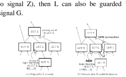
to signal Z), then L can also be guarded by signal G.
Network before and after guarding
Since L's single fan out is to Z, L's output value will not affect overall circuit outputs when G is logic-0. Toggles that occur in computing L's output when G is logic-0 are an unnecessary waste of dynamic power. In figure 3.1(a), L is a candidate for guarded evaluation by signal G. If LUT L has a free input, we modify the mapped network by attaching G to L, and then modifying L's logic functionality as shown in figure 3.1(b). The question is how to modify L's logic functionality. In, logic functions were modified to force the LUT output to a logic-0when guarded. Here we also consider different types of guards based on signal probabilities and guarding values. For a signal L, define its static probability, P(L), as the probability that the signal is logic-1. Static probability is a property of logic signals widely used in the power estimation domain. Assume a guarding value of logic-0 for signal G; the new logic function for L is determined based on L's static probability, P(L), of signal L. If the signal spends most of its time at logic-0 (i.e., P(L)=0:5), it is set equal to a logical AND of its previous logic function and signal G. Hence, we force the signal to logic-0 when It is guarded. If P(L) > 0:5, the logic function is set equal to the logical OR of the previous logic function and the inverted version of signal G, hence forcing the signal to logic-1 when it is guarded.
This distinction is made to avoid inducing additional toggles on the guarded signal. Consider the case where the output of LUT L in
figure 3.1(b) was logic-1 the instant prior to guarding. If it was guarded using a logical AND of its previous function and signal G, then the gate would induce one additional toggle from logic-1 to logic-0. Hence, the static probability of the guarded signal is examined prior to inserting the guarding logic to avoid such additional (and unnecessary toggles).
Modified function internal to LUTs
The guarded evaluation procedure can be applied recursively by walking the mapped network in reverse topological order. For example, after considering guarding LUT L with signal G, we examine L's fan in LUTs and consider them for guarding by G. Since LUT N in figure 3.1(a) only drives LUT L, N is also a candidate for guarding by signal G. We traverse the network to build up a list of guarding options. There may exist multiple guarding candidates for a given LUT. For example, if signal H in figure 3.1(a) were a gating or trimming input to LUT L, then H is also a candidate for guarding LUT N (in addition to the option of using G to guard N). Furthermore, if a LUT has multiple free inputs, we can guard it multiple times. The ease with which we can use AIGs to identify gating and trimming inputs (via finding inverting and partial non-inverting paths) circumvents one of the key difficulties encountered by specifically, problem of determining which signals can be used to guard which gates.
Overview ASIC Design Introduction
International Journal of Research (IJR)
e-ISSN: 2348-6848, p- ISSN: 2348-795X Volume 2, Issue 10, October 2015Available at http://internationaljournalofresearch.org
specification of the flip flops. This is where Synopsys’s Prime Time comes into the ASIC design flow. Prime Time is a full chip static analysis tool that can fully analyze a multimillion gate ASIC in a short amount of time. The main advantage of Prime Time is that does not use test vectors to simulate the critical path. This vector-less approach removes the possibility that not all critical paths are identified when writing the delay vectors. With many of the commands the same as Design-Compiler, making the addition of Prime Time to the ASIC design flow very easy because the designer does not have a steep learning curve. Prime Time has the ability to analyze a design over various temperatures, voltages, and process variations, will make a designer feel that they have produced a very robust design.
LOW POWER TECHNIQUES Clock Gating
Clock gating is a popular technique used in
many synchronous circuits for reducing
dynamic power dissipation. Clock gating saves power by adding more logic to a circuit to prune the clock tree. Pruning the clock disables portions of the circuitry so that the flip-flops in them do not have to switch states. Switching states consumes power. When not being switched, the switching power consumption goes to zero, and only leakage currents are incurred. Clock gating works by taking the enable conditions attached to registers, and uses them to gate the clocks. Therefore it is imperative that a design must contain these enable conditions in order to use and benefit from clock gating.
Block Diagram of Gated Clock
The disconnecting of the clock from a device it drives when the data going into the device is not changing. This technique is used to minimize dynamic power.
CONCLUSION AND FUTURE SCOPE
In this project, the various digital designs and especially sequential circuits are used main aim is reducing the dynamic power and leakage power. This paper is implementing in FPGA’s only the different FPGA powers are required only use cad tools can required RTL power. Using Clock gating we can reduce the dynamic power consumed. We must be able to reduce leakage power.Spartan3 based on 40 nm technology. Latest Cad tool techniques are based on 180 nm technology which contributes certain leakage power. So, there is need to reduce this leakage dynamic power along with dynamic power. The future scope of the project is reducing the delays and increasing the speed of the system on chip.
REFERENCES
[1] S. Jang, K. Chung, A. Mishchenko, and R. Brayton, ―A power optimization toolbox for logic synthesis and mapping,‖ in Proc. IEEE Int. Workshop Logic
[2] V. Tiwari, S. Malik, and P. Ashar,
―Guarded evaluation: Pushing power
International Journal of Research (IJR)
e-ISSN: 2348-6848, p- ISSN: 2348-795X Volume 2, Issue 10, October 2015Available at http://internationaljournalofresearch.org
[3] J. Anderson and Q.Wang, ―Improving logic density through synthesis-inspired architecture,‖ in Proc. IEEE Int. Conf. Field-Programmable Logic Applicat., Aug.–Sep. 2012, pp. 105–111.
[4] A. Mishchenko. (2012). ABC: A System for Sequential Synthesis and Verification [Online].
[5] Clock-Gating and Its Application to Low Power Design of Sequential Circuits Qing WU Department of Electrical Engineering-Systems, University of Southern California Los Angeles,
CA 90089, USA. Available:
http://www.eecs.berkeley.edu/∼alanmi/abc
[6] Altera Corporation. (2009). Quartus-II
University Interface Program [Online].
Available:http://www.altera.com/education/univ /research unv-quip.html
[7] Automatic synthesis of clock gating logic with controlled netlist perturbation Hurst, A.P. Design Automation Conference, 2008. DAC 2008. 45th ACM/IEEE Publication Year: 2008.
[8] Symbolic synthesis of clock-gating logic for
power optimization of control-oriented
synchronous networks Benini, L. ; De Micheli, G. ; Macii, E. ; Poncino, M. ; Scarsi, R. European Design and Test Conference, 1997. ED&Tc97.Proceedings Publication Year: 1997.
[9] D. Howland and R. Tessier, ―RTL dynamic power optimization for FPGAs,‖ in Proc. IEEE Midwest Symp. Circuits Syst., Aug. 2008, pp. 714–717. Synthesis, Aug. 2009, pp. 1–8.