ISSN (Print) : 2320 – 3765 ISSN (Online): 2278 – 8875
I
nternational
J
ournal of
A
dvanced
R
esearch in
E
lectrical,
E
lectronics and
I
nstrumentation
E
ngineering
(An ISO 3297: 2007 Certified Organization)
Vol. 4, Issue 4, April 2015
High Performance and Low Noise BCD Adder
Circuit Design Using Rate Sensing Keeper
S.Rambabu
1, B.Sruthi
2, K.Sreelakshmi
3, V.Ramyakrishna
4, S.Althaf
5, K.Subash
6Assistant Professor, Dept. of E.C.E, Santhiram Engineering College, Nandyal, AP, India 1
IV-B.Tech Students, Dept. of E.C.E, Santhiram Engineering College, Nandyal, AP, India 2
IV-B.Tech Students, Dept. of E.C.E, Santhiram Engineering College, Nandyal, AP, India 3
IV-B.Tech Students, Dept. of E.C.E, Santhiram Engineering College, Nandyal, AP, India 4
IV-B.Tech Students, Dept. of E.C.E, Santhiram Engineering College, Nandyal, AP, India 5
IV-B.Tech Students, Dept. of E.C.E, Santhiram Engineering College, Nandyal, AP, India 6
ABSTRACT: The basic factors which affect any VLSI circuit design are area, speed and power consumption. Full adder is a basic element used in multiplexers, processor designs. Full adders can be implemented using CMOS technology. The CMOS technology plays a major role on the performance of microprocessors on very large scale integrated circuits chips. In this paper Full adder circuit is designed based on conventional domino logic using "Rate sensing keeper" technique. This technique helps to achieve high speed, low noise than conventional CMOS. The full adder circuit design using "Rate Sensing Keeper" gives superior performance compared to Full adder circuits designed using other techniques. In this finally implement BCD adder by using Full adder circuit is designed based on conventional domino logic with "Rate sensing keeper" technique. on mentor graphics tool 130 nm technology.
KEYWORDS
:
CMOS, Domino logic, Rate sensing keeper technique, scaling technologyI.INTRODUCTION
CMOS technology plays a major role on the performance of VLSI circuits .The timing performance of the microprocessor can be improved by using dynamic circuits in microprocessors. However the usage of dynamic circuits in microprocessors is limited due to many challenges including transistor sizing, charge sharing, leakage current, noise immunity etc .Timing optimization of dynamic circuits can be achieved through several methods such as transistor sizing, using multiple threshold voltages etc..The aggressive scaling of transistors and interconnect dimensions has caused noise to become an increasingly important issue in integrated circuit design. A number of design techniques have been proposed to enhance the noise tolerance of domino logic circuit. The delay of the dynamic circuits can be controlled by varying the sizes of transistors in the circuit. The circuit delay can be reduced by increasing the transistor sizes in the circuit. This means that high speed circuits require larger area. So for dynamic circuits, there is a trade off exist between speed and area. Domino logic circuits are the most widely used dynamic logic style. Domino logic circuits have two phases of operations-first phase called precharge phase and second phase called evaluation phase. During the precharge phase of the domino logic circuits, the clock remains low and the dynamic node is precharge to V DD through a p-type pull up transistor. The evaluation phase starts when the clock transit from low to high and during this phase the pull down network evaluates the logic function.
ISSN (Print) : 2320 – 3765 ISSN (Online): 2278 – 8875
I
nternational
J
ournal of
A
dvanced
R
esearch in
E
lectrical,
E
lectronics and
I
nstrumentation
E
ngineering
(An ISO 3297: 2007 Certified Organization)
Vol. 4, Issue 4, April 2015
circuits. The rate sensing keeper (RSK) technique based full adder circuit work based on the difference in the rate of change of voltage at the dynamic node of the gate during the ON and the leakage condition. The state of the keeper is controlled by a reference rate which is the average of the rate of change of voltage at the dynamic node of the gate during the ON and the leakage condition. One method to reduce the sub threshold leakage current in domino circuits is the usage of diode footer. The diode footer reduces the sub threshold leakage current in the domino circuit due to a phenomenon called the stacking effect . A voltage drop will be established across the diode footer in the evaluation phase due to the leakage of the evaluation transistors in the pull down network.
The paper is organized as follows. Section II Existed method full adder and Section III operation of the full adder using RSK technique. Section IV Simulation result and Section V Conclusion
II. EXISTED METHOD FULL ADDER
In which, the full adder is implemented based on domino logic technique. The basic logic diagram of domino logic is shown in below fig (a)
Fig(a) basic logic diagram of domino logic
The above fig(a) shows the basic domino logic inverter diagram that operate in two modes one is precharged which is occur when clock is low and another one is evaluation which is occur when clock is low. The below fig (b)&(c) shows the domino logic based sum and carry MENTORGRAPHICS TOOLS 130 nm technology
fig(b): the domino logic based sum
ISSN (Print) : 2320 – 3765 ISSN (Online): 2278 – 8875
I
nternational
J
ournal of
A
dvanced
R
esearch in
E
lectrical,
E
lectronics and
I
nstrumentation
E
ngineering
(An ISO 3297: 2007 Certified Organization)
Vol. 4, Issue 4, April 2015
It provides low power dissipation than CMOS but add noise in the result. Hence in order to control that, in this paper modified the above adder with rate sensing keeper technique shown in below proposed method
III. PROPOSED METHOD FULL ADDER
In order to overcome the noise and leakage power in the above existed domino logic and achieve the high speed, for that modified the above circuit with rate sensing keeper technique shown in below fig. this proposed method gives the better performance compared to all existed methods.
The Domino logic with Rate sensing keeper technique based full adder is shown in below implemented based on MENTORGRAPHICS TOOLS 130 nm technology
Fig: Domino logic with Rate sensing keeper technique based full adder
A.BCD ADDER IMPLEMENTATION
ISSN (Print) : 2320 – 3765 ISSN (Online): 2278 – 8875
I
nternational
J
ournal of
A
dvanced
R
esearch in
E
lectrical,
E
lectronics and
I
nstrumentation
E
ngineering
(An ISO 3297: 2007 Certified Organization)
Vol. 4, Issue 4, April 2015
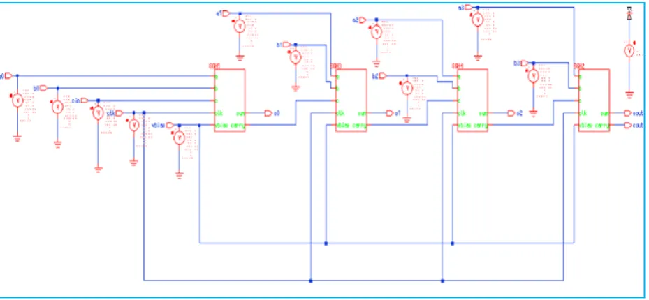
For implementation of the above circuit, used two 4-bit binary adders and two AND, one OR gates. The implementation of 4-bit binary adder is shown in below fig implemented based on mentor graphics tools. Here, we interconnected four full adders to formed one 4-bit binary adder
Fig: 4-bit binary adder
IV. SIMULATION RESULT
The simulations are performed based on mentor graphics tools with 130nm technology. The below fig(a)&(b) shows the resultant wave forms of domino logic based full adder sum and carry.
Fig (a) fig (b)
ISSN (Print) : 2320 – 3765 ISSN (Online): 2278 – 8875
I
nternational
J
ournal of
A
dvanced
R
esearch in
E
lectrical,
E
lectronics and
I
nstrumentation
E
ngineering
(An ISO 3297: 2007 Certified Organization)
Vol. 4, Issue 4, April 2015
Fig(c) Fig(d)
From the above fig(c)&(d) we observed that, reduced noise in output sum and carry waveforms compared to fig(a) and (b). The output noise decreases with increase in bias voltage. But the increase in bias voltage also increases the circuit delay. So the selection of bias voltage plays a major role in the circuit operation. The full adder circuit implemented based on an adaptive keeper technique called rate sensing keeper (RSK) that enables faster switching and the experimental results shows that the full adder circuit designed using rate sensing keeper transistor technique gives superior performance compared to the other alternatives
V. CONCLUSION
In this paper the performance of a full adder circuit designed using rate sensing keeper transistor technique is analyzed in detail and its performance is compared with other full adder circuits. The full adder circuit is simulated using MENTORGRAPHICS TOOLS on 130nm. The experimental results shows that the full adder circuit designed using rate sensing keeper transistor technique gives superior performance compared to full adder circuits designed using conventional domino techniques. The performance of the wide fan in circuits implemented using domino logic technologies can be further improved by using Fin FET devices. Another advantage of using Fin FET is its high scalability and low leakage power compared to conventional MOSFETs.
REFERENCES
[I] World's First 2-Billion Transistor Microprocessors Intel Corporation. Feb. 2008 [Online]. Available: http://www.intel.com/technology/ architecture silicon! 2billion.htm?iid=tech_micro+2b.
[2] D. H. Allen. S. H. Dhong, H. P. Hofstee, 1. Leenstra, K. J. Nowka, D. L. Stasiak, and D. F. Wendel, "Custom circuit design as a driver of microprocessor performance," iBM J. Res. and Develop., vol. 44, no. 6, pp. 799-822, Nov. 2000.
[3] P. E. Gronowski, W. J. Bowhill, R. P. Preston, M. K. Gowan, and R. L. Allmon, "High-performance microprocessor design," iEEE J. Solid- State Circuits, vol. 33, no. 5, pp. 676-686, May 1998. [4] K. Yelamarthi and c.-I. H. Chen, "Process variation- aware timing optimization for dynamic and mixed-static-dynamic CMOS logic," iEEE Trans. Semicond. Manuf, vol. 22, no. I, pp. 31-39, Feb. 2009.
[5] 1. P. Fish burn and A. E. Dunlop, "TlLOS: A posynomial programming approach to transistor sizing," in into Con] Computer Aided Design, 1985, pp. 326-328.
[6] V. Sundararajan, S. S. Sapatnekar, and K. K. Parhi, "Fast and exact transistor sizing based on iterative relaxation,"iEEE Trans. Comput.- Aided Design integr.Circuits Syst., vol. 21, pp.568-581,May-2002.
[7] M. Zhao and S. S. Sapatnekar, 'Timing-driven partitioning and timing optimization of mixed static-domino implementations, “iEEE Trans. Comput.-Aided Design integr. Circuits Syst., vol. 19, no. II, pp. 1322-1336, Nov. 2000.