FPGA Based Speed Control of Single Phase
Induction Motor by Using PWM Technique
Amagoth Venugopal Naik1, Venkatesha K2, Varsha Tatti3
M. Tech Student (CAID), Dept. of EEE, BNM Institute of Technology, Bangalore, India1
Associate Professor, Dept. of EEE, BNM Institute of Technology, Bangalore, India2
Assistant Professor, Dept. of EEE, BNM Institute of Technology, Bangalore, India 3
ABSTARCT: Inverters are circuits that convert DC source into AC source. These DC-AC inverters have been widely used for industrial applications such as motor speed control, output voltage control, Emergency power supply, uninterruptible power supply (UPS),etc.Power switches are used in inverter with UNIPOLAR SPWM techniques. The SPWM techniques reduce harmonics and improve fundamental. It also reduces THD of voltage. Another important thing is to design the control circuit to provide switching signal to the power circuit. The control circuit consist of FPGA kit, opto-coupler, and voltage amplification. The Power Circuit consist of MOSFET Switches. A field-programmable gate array (FPGA) is an integrated circuit designed to be configured by a customer or a designer after manufacturing. The FPGA Real time controller is used to generate PWM pulses at different frequencies by different carrier frequencies. The modulation index is varied by varying the amplitude of the reference or sine wave. These switching pulses are given to four switches of the inverter. The rms output of the inverter is varied by varying modulation index. The harmonic profile of output voltage of the inverter is varied by changing the carrier frequency. Simulation is carried out using MATLAB Simulink, the hardware results and simulation results are compared.
KEYWORDS: FPGA, pulse width modulation, total harmonic distortion, speed control
I. INTRODUCTION
In present years, microcontrollers, Digital Signal Processors (DSPs), DSP IC been widely used implementing control motor algorithms in industry. But it has some disadvantages like, long development period and poor software portability and re-usability. Any changes in the program, imposed in the introduction to the need of good performance or new features require a large change to the project, to fit with the new system. To satisfy these demands a FPGA based hardware implementation technology is used. For three phase induction motor speed control, AC motor drives Pulse Width Modulation (PWM) inverters used in drive applications. Both the magnitude and frequency of the applied voltage to a motor can be controlled by PWM inverters.
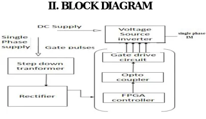
II. BLOCK DIAGRAM
Fig1. Block Diagram
A PWM based VSI is used to convert the DC link voltage to the required AC voltages and frequency. The PWM inverter has four MOSFET switches that are controlled in order to generate an AC output from the DC input. In the present scheme, the SPWM pulses are generated using a software program coded with VHDL and downloaded in FPGA kit to produce gate signals for inverter MOSFET switches. This signal coming from the FPGA controller can't feed directly to the MOSFET gate pin due to the weakness of its voltage (3.3V). The voltage shifting from 3.3V to 12V requires a gate driver circuit. The basic block diagram is shown in Fig. 1The variation in the duty cycle and the number of SPWM pulses determines the amplitude and frequency of the inverter. This can be achieved by varying either the amplitude or frequency of the carrier signal (triangular wave). A model for the controller was designed using VHDL.
III. DESIGN SPECIFICATION
Output Voltage : Single-phase 24VAC RMS Output Frequency : 50Hz
Output Power Range : <500Watts
Switching Frequency : Variable frequency, Variable duty cycle Controllers : FPGA kit
III. FIELD PROGRAMMABLE GATE ARRAY (FPGA)
Logic circuitry of FPGA consist of arrays of gate and reconfigurable matrix block. The application of software and implementation of hardware is creates when the blocks configured. To process the logic it uses logic of particular hardware processing unlike other OS. Other process need not to be compete as it ids parallel in nature. because of this if there is more loops are logically controlled and performing it doesn’t affects the output performance. the FPGA are allows their internal circuit to be reconfigured and hence the control circuit performance increases.
IV.PULSE WIDTH MODULATION (PWM)
Pulse-width modulation (PWM), or pulse-duration modulation (PDM), is a modulation technique that controls the width of the pulse, formally the pulse duration, based on modulator signal information. Although this modulation technique can be used to encode information for transmission, its main use is to allow the control of the power supplied to electrical devices, especially to inertial loads such as motors.
The average value of voltage (and current) fed to the load is controlled by turning the switch between supply and load on and off at a fast pace. The longer the switch is on compared to the off periods, the higher the power supplied to the load.The PWM switching frequency has to be much higher than what would affect the load (the device that uses the power), which is to say that the resultant waveform perceived by the load must be as smooth as possible. Typically switching has to be done several times a minute in an electric stove, 120 Hz in a lamp dimmer, from few kilohertz (kHz) to tens of kHz for a motor drive and well into the tens or hundreds of kHz in audio amplifiers and computer power supplies.
Fig 4PWM signals of varying duty cycles
V. SPWM INVERTER
In SPWM inverter the output voltage is gating by comparing the reference signal and carrier signal at the desired frequency as shown in figure 5. During first half cycle the output voltage is having positive value when reference signal having more amplitude then carrier signal. In the another half cycle the output voltage is having negative value when reference signal having less amplitude then carrier signal. The control frequency depends on pulse per half cycle and the output frequency depends on reference frequency. The basic operation circuit of single phase SPWM inverter is as shown in figure 6.
S1 is on when Vr>Vc
S2 is on when -Vr<Vc
S1 is on when -Vr>Vc
S2 is on when Vr<Vc
As shown above, if we use switching scheme then we can generate high frequency signal and harmonic free output voltage control. Hence we have the controllable output voltage and smooth speed control of single phase AC Motor.
Single phase inverter with RL-load
Fig.6: Operation of single phase inverter with RL load
During positive half cycle, modulating signals are given to switch S1 and S4 is turned ON using ZCD pulses. S2 and S3 is turned off. This is shown in Fig.6.
During negative half cycle, modulating signals are given to switch S3 and S2 is turned ON using NZCD pulses where as S1and S4 are turned off.
VI. SOFTWARE IMPLEMENTATION
This paper represents three phase induction motor drive of FPGA based controller using PWM speed control method. VHDL language is used to program the Sparten-6 FPGA. Xilinx ISE Design Suite 12.1 is used as software to write coding. Sparten 6 development board has 20MHz clock signal by default i.e. each clock cycle is 50ns. The firmware code is developed based on this frequency.
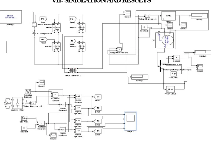
VII. SIMULATION AND RESULTS
Fig 7 simulink diagrm
S
3For simulation MATLAB/SIMULINK is used and simulation is verified for this drive at various set speed. This drive system consists of four switches single phase inverter and single phase squirrel cage Induction Motor. Supply voltage: 1-phase, 230 V (rms), 50 Hz. 1450 rpm. The full Simulink block diagram o is shown in Fig.6. The output line voltage and current waveform of inverter is shown in Fig.9, 10 and 11, The stator currents and torque waveforms shown in Fig. 13The speed characteristics of induction motor are shown in Fig.12. It is observed that the speed increases linearly and reaches the set speed at steady state.At starting the the torque increases and reduces to a minimum value when the speed reaches the set value.
Fig.. 8 Switching pulses Fig.9.Input current waveform for the inverter
Fig.10.Output voltage waveform of the inverter. Fig.11.Output current waveform of the inverter.
TABULAR REPRESENTATION OF RESULTS
Tabular results obtained by performing simulation for frequencies 1.7khz,2.1khz,2.5khz and 2.7khz is as shown in table number.1,2,.3 and 4 respectively.
Table no 1 .For frequency 2.1KHZ Table no.2.For frequency 1.7KHZ
Table no.3.For frequency 2.5KHZ Table no.4.For frequency 2.7KHZ
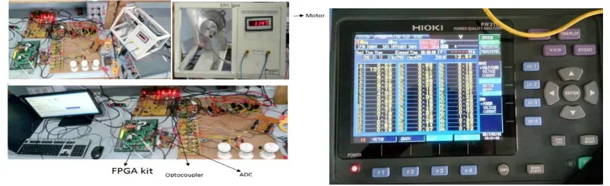
VIII. HARDWARE IMPLIMENTATION
In hardware implimentation the speed control is achieved by controlling the switching pulses for the inverter andharmonics are reduced selectively. IPFPE50 mosfet switches are used for inverter design, MCT2E and ICTC4424used in optocoupler circuit, ADC0804 used for converting analog signal to digital signal, op-amo LM349 used as acomparator in ZCD circuit.the FPGA has inbuilt DAC to produce triangular waveform. The results obtained from the hardware implementation is as shown below,
Fig.18.Speed V/S modulation index Fig.19.THD V/S modulation index
VIII. CONCLUSION
The FPGA Real time controller is used to generate PWM pulses at different frequencies by different carrier frequencies. The modulation index is varied by varying the amplitude of the reference or sine wave. These switching pulses are given to four switches of the inverter. The rms output of the inverter is varied by varying modulation index. The harmonic profile of output voltage of the inverter is varied by changing the carrier frequency. Simulation is carried out using MATLAB Simulink. The hardware results obtained is conformed with the simulation results obtained.
IX. FUTURE SCOPE
This work can be extended further for implementing SVPWM technique. In SVPWM methods, a revolving reference voltage vector is provided as voltagereference instead of three phase modulating waves. The magnitude and frequency of the fundamental component in the line side are controlled by the magnitude and frequency, respectively, of the reference vector. The highest possible peak phase fundamental is very less in sine triangle PWM when compared with space vector PWM.Total harmonic distortion (THD) can be reduced in fundamental component of voltage using SVPWM technique compared to sinusoidal PWM.
REFERENCES
[1]S.Mekhilef and N.A.Rahim,"XILINX FPGA three-phase PWM inverterand its application for utility connected PV system"in Proc.IEEE.TENCO'02, 2002, pp.2079-2082.
[2] Ying-Yu Tzou, Tien Sung Kuo,” Design and Implementation of FPGAbaseMotor control IC for Permanent magnet AC servo motors” IEEE Transaction on Industrial Electronics, Vol.38, No.2, 1996.
[3] Y.Y.Tzou, MIEE, and H.J.Hsu,” FPGA Realization of Space –VectorPWM control IC for Three Phase PWM Inverter,” IEEE TransactionsonPower Electronics, vol.12, no.6, pp953-963, Nov.1997.
[4] R.M.Jalnekar and Mrs K.S.Jog “Pulse-Width-Modulation Techniques for switched Mode inverters”, NSDES-97, 27-28 Nov 1997, pp 118-124. [5]Holtz 1.," Pulse Width Modulation For Electronic Power Conversion", Proceed inp of the IEEE. Vot.12, No.1,AUI. 199400.1194..1214.
[6] R. Dubey, P. Agarwal, and M. K. Vasantha, “Programmable logicdevices for motion control-A review,” IEEE Trans. Ind. Electron., vol. 54,no. 1, pp. 559-566, 2007.
0 0.5 1 1.5 2
0.5 0.7 0.9
1.7Khz 2.1Khz 2.5Khz 2.7Khz 0 0.5 1 1.5 2
0.5 0.7 0.9
1.7Khz 2.1Khz 2.5Khz 2.7Khz 0 500 1000 1500 2000
0.5 0.7 0.9