DOI: 10.15662/ijareeie.2014.0307010
Copyright to IJAREEIE www.ijareeie.com 10455
Five-Input Complex Gate with an Inverter
Using QCA
Tina Suratkar1
Assistant Professor, Department of Electronics & Telecommunication Engineering, St.Vincent Pallotti College Of
Engineering and Technology, Nagpur, Maharashtra, India1
ABSTRACT:This paper presents the basics of quantum dot cellular automata along with the QCA logic devices such as the QCA wire, inverter and the majority gate. The four phases of the clocking have been discussed and also the implementations of the complex gate have been done using the QCADesigner tool. The logical structures such as NAND and NOR gates using a quantum dot cellular automata complex gate composed of 3 input majority gate and an inverter have been implemented.
KEYWORDS: QCA, majority gate, inverter, complex gates, QCA Designer.
I.INTRODUCTION
Current silicon transistor technology faces challenging problems, such as high power consumption and difficulties in feature size reduction. Nanotechnology is an alternative to these problems. The Quantum dot cellular automata (QCA) is one of the attractive alternatives [1]. Since QCAs were introduced in 1993 by lent et al, and experimentally verified in 1997. QCA is expected to achieve high device density, extremely low power consumption and very high switching speed.QCA structures are constructed as an array of quantum cells with in which every cell has an electrostatic interaction with its neighboring cells [2]. QCA applies a new form of computation, where polarization rather than the traditional current, contains the digital information. In this trend, instead of interconnecting wires, the cells transfer the information throughout the circuit [4].
This paper describes the design of different logical structures in QCA such as NAND and NOR. These structures are designed based on the basic logical devices. The paper is organized as follows, the background of QCA technology is explained in section 2. Section 3, provides the QCA clocking and section 4 describes the QCA Designer tool. Section 5 shows the design and implementation of logical structures in QCA using three input majority and an inverter. Simulation results follow in section 6 and conclusions are presented in section 7.
II.
BACKGROUNDA. QCA basics
QCA technology is based on the interaction of bi-stable QCA cells constructed from four quantum dots. The cell is charged with two free electrons, which are able to tunnel between adjacent dots. These electrons tend to occupy antipodal sites as a result of their mutual electrostatic repulsion. Thus, there exist two equivalent energetically minimal arrangements of the two electrons in the QCA cell, as shown in Fig. 1. These two arrangements are denoted as cell polarization P= +1and P= -1.By using cell polarization P =+1 to represent logic “1” and P =-1 to represent logic “0,” binary information is encoded in the charge configuration of the QCA cell [2][5].
DOI: 10.15662/ijareeie.2014.0307010
B. QCA logic devices
The fundamental QCA logic primitives include a QCA wire, QCA inverter, and QCA majority gate[4]-[6], as described below.
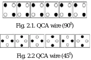
QCA Wire: In a QCA wire, the binary signal propagates from input to output because of the electrostatic interactions between cells. The propagation in a 90˚ QCA wire is shown in Fig. 2. Other than the 90˚ QCA wire, a 45˚ QCA wire
can also be used. In this case, the propagation of the binary signal alternates between the two polarizations [4].
Fig. 2.1. QCA wire (900)
Fig. 2.2 QCA wire (450)
QCA inverter: The QCA cells can be used to form the primitive logic gates. The simplest structure is the inverter shown. Fig. 3, which is usually formed by placing the cells with only their corners touching. The electrostatic interaction is inverted, because the quantum-dots corresponding to different polarizations are misaligned between the cells [3].
Fig. 3.QCA inverter
QCAMajorityGate:
TheQCAmajoritygateperformsathree-inputlogicfunction.AlayoutofaQCAmajoritygateisshowninFig.4.1.Assumingtheinputsarea,bandc,thelogicfunctionofthe majoritygateis
M(a,b,c)=ab+bc+ac.(1)
Fig.4.1.QCAmajoritygate
Thetendencyofthemajoritydevicecelltomovetoagroundstateensuresthatittakesonthepolarizationofthemajorityofitsneighb ours.Thedevicecellwilltendtofollowthemajoritypolarizationbecauseitrepresentsthelowestenergystate[3].Byfixingthepola rizationofoneinputtotheQCAmajoritygateaslogic “1” orlogic “0” anANDgateorORgatewillbeobtained,respectively,asshowninFig.4.2.
DOI: 10.15662/ijareeie.2014.0307010
Copyright to IJAREEIE www.ijareeie.com 10457 III.CLOCKING
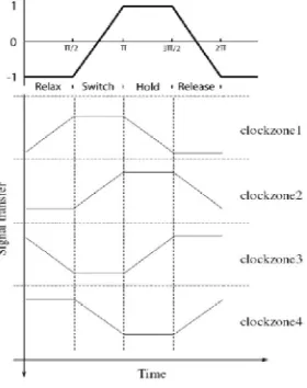
TheQCAcircuitsrequireaclock,notonlytosynchronizeandcontrolinformationflowbutalsotoprovidethepowertorunthecircui tsincethereisnoexternalsourceforpoweringcells.Withtheuseoffourphasesclockingschemeincontrollingcells,QCAprocesse sandforwardsinformationwithincellsinanarrangedtimingscheme.Cellscanbegroupedintozonessothatthefieldinfluencingal lthecellsinthezoneswillbethesame.Azonecyclesthrough4phases.IntheSwitchphase,thetunnelingbarriersinazoneareraised. Whilethisoccurs,theelectronswithinthecellcanbeinfluencedbytheColumbicchargesofneighboringzones.ZonesintheHoldp hasehaveahightunnelingbarrierandwillnotchangestate,butinfluenceotheradjacent.Lastly,theReleaseandRelaxdecreasethe tunnelingbarriersothatthezonewillnotinfluenceotherzones.Thesezonescanbeofirregularshape,buttheirsizemustbewithince rtainlimitsimposedbyfabricationanddissipationconcerns.Properplacementofthesezonesiscriticaltodesignefficiency.Thiscl ockingmethodmakesthedesignofQCAdifferentfromCMOScircuits.[7].
TheFig.5.Showsthefouravailableclocksignals.Eachsignalisphaseshiftedby90˚degrees.Whentheclocksignalislowthecellsa relatched.Whentheclocksignalishighthecellsarerelaxedandhavenopolarization.Inbetweenthecellsareeitherlatchingorrelax ingwhentheclockisdecreasing/increasingrespectively.
Fig. 5.Four phases of the clock.
IV.QCA DESIGNER TOOL
QCA logic and circuit designers require a rapid and accurate simulation and design layout tool to determine the functionality of QCA circuits. QCADesigner gives the designer the ability to quickly layout a QCA design by providing an extensive set of CAD tools. As well, several simulation engines facilitate rapid and accurate simulation. It is the first publicly available design and simulation tool for QCA. Developed at the ATIPS Laboratory, at the University of Calgary, QCADesigner currently supports three different simulation engines, and many of the CAD features required for complex circuit design. [8],[9].
V. QCA IMPLEMENTATION
The AND and OR gates are realized by fixing the polarization to one of the inputs of the majority gate to either P=-1(logic 0) or P=P=-1(logic 1).
cell-DOI: 10.15662/ijareeie.2014.0307010
inverter is created by translating the output cell ‘Y’ by 9 nm horizontally. The functionality of this gate for four input NAND and NOR configurations has been simulated using QCA Designer. Fig. 6 shows five-input complex gate with a majority gate placed in the middle and a two cell-inverter made by translating the output Y.
Fig.6 Five-Input complex gate with an inverter
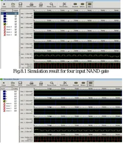
A. Four-Input NAND Gate
The five-input gate of Fig. 6 can be used to form a 4-input NAND gate as shown in Fig. 7.1 by restricting input e to have a fixed polarity that is equal to -1. The selection of e is unique, either a or b can be restricted rather than e, and similarly c or d can be selected for restriction rather than g. For the example circuit as shown in Fig. 8, the function represented is Y=abcd
Fig.7.1 Four input NAND gate
B. Four-Input NOR Gate
DOI: 10.15662/ijareeie.2014.0307010
Copyright to IJAREEIE www.ijareeie.com 10459
Fig. 7.2 Four input NOR gate
VI.SIMULATION RESULTS
With QCADesigner, the circuit functionality is verified. The following parameters are used for a bistable approximation: Cell size 18nm, Number of samples 12800, Convergence tolerance 0.001000, Radius of effect 65nm, Relative permittivity 12.9, Clock high 9.8e-22J, Clock low3.8e-23J, Clock amplitude factor2, Layer separation 11.5nm, Maximum Iterations per sample 100.
Fig.8.1 Simulation result for four input NAND gate
DOI: 10.15662/ijareeie.2014.0307010
VII.CONCLUSION
The logical structures such as NAND and NOR using five-input complex gate composed of a 3-input majority gate and a two cell inverter have been designed. One of these inputs typically function as control inputs to determine the logical structure formed by the four other inputs to the circuit. This five-input gate can be configured as a four-input NAND gate and a four-input NOR gate which are verified through simulation results.
REFERENCES
[1] C.S.Lent, P.D.Tougaw, W.Porod, and G.H.Bernstein, “Quantum cellular automata, “Nanotechnology, vol.4, no.1, pp.49–57, January1993. [2] P.D.Tougaw, C.S.Lent, and W.Porod, “Bistable saturation in coupled quantum-dot cells, ”Journal of Applied Physics, vol.74, no.5, pp.3558–
3566, September1, 1993.
[3] P.D.Tougaw and C.S.Lent, “Logical devices implemented using quantum cellular automata, ”Journal of Applied Physics, vol.75, no.3, pp.1818–1825, February1, 1994.
[4] C.S.Lent and P.D.Tougaw, “Lines of interacting quantum-dot cells: A binary wire, ”Journal of Applied Physics, vol.74, no.10, pp.6227–6233, November15, 1993.
[5] C.S.Lent, P.D.Tougaw, and W.Porod, “Bistable saturation in coupled quantum dots for quantum cellular automata, ”Applied Physics Letters, vol.62, no.7, pp.714–716, February 15, 1993.
[6] C.S.Lent and P.D.Tougaw, “A device architecture for computing with quantum dots, ”Proceedings of the IEEE, vol.85, no.4, pp.541–557, April 1997.
[7] S.Karthigai Lakshmi, G.Athisha, “Efficient design of logical structures and functions using nanotechnology based quantum dot cellular automata design,” International Journal of Computer Applications, vol.3, no.5, (0975-8887), June 2010.
[8] QCADesigner, version 1.3.2. Available at http://www.atips.ca/projects/qcadesigner/.