DESIGN OF HIGH SPEED AND POWER
EFFICIENT DOUBLE TAIL
COMPARATOR
G. Divya
Department of Electronics and Communication, Maharaj Vijayaram Gajapathi Raj College of Engineering
Email: [email protected]
Mr. D. Raja Ramesh
Department of Electronics and Communication, Maharaj Vijayaram Gajapathi Raj College of Engineering
Email: [email protected]
Abstract
High speed dynamic regenerative comparators are used in low power and area efficient analog to digital converters to improve speed and power efficiency. Speed and power consumption are the two factors that can define the comparators accuracy. In this paper, a double tail comparator is proposed by modifying the low voltage low power double tail comparator circuit for power efficient and high speed operation. In the Proposed dynamic Double tail comparator system both the power dissipation and delay time will be significantly reduced. By reducing clock overhead in the double tail comparator delay and area can be reduced. The circuits presented in this paper are designed in 130nm technology by using mentor graphics tools with a supply voltage of 0.8v and 0.6v. Proposed comparator is compared with existing double tail comparator and the results are discussed in detail.
Keywords: Analog to digital converters, Double tail comparator, Dynamic regenerative comparators, and low power analog design.
1. Introduction
Comparator is a circuit that compares an analog signal with a reference voltage or with another analog signal and outputs a binary signal based on the comparison. In most analog to digital converters comparators are the fundamental building blocks. Output of the comparator is logic 1 when the positive input of it is at higher value than the input at the negative terminal and vice versa. Comparators are widely used in the process of converting analog signals to digital signals. In analog to digital conversion process it is necessary to sample the input first. To determine the digital equivalent of the analog signal the sampled signal is then applied to a combination of comparators. In its simplest form, a comparator can be considered as a 1-bit analog to digital converter.
Design of high speed comparators to operate at small supply voltages is more difficult. In ultra deep sub micrometer (UDSM) CMOS technologies high-speed comparators suffer from low supply voltages [2]. To obtain high speed and to compensate the supply voltage reduction, larger transistors are required that means more chip area and power is required. In high speed analog to digital converters common mode input range is very important but it is limited at low voltage operations. To meet the low-voltage design challenges supply boosting methods and techniques employing body-driven transistors [9] and current-mode design [10] have been developed.
Developing circuit structures which avoid stacking too many transistors between the supply rails is preferable for low voltage operations. A new dynamic double tail comparator was implemented, which does not require stacking of too many transistors, which resulted in positive feedback strengthening in latch stage. Based on the previously proposed double tail comparator, in this paper a new dynamic comparator is designed. The delay and power dissipation are reduced in proposed comparator as compared to conventional double tail comparator [4].
2. Existing Comparators
2.1. Conventional Dynamic Comparator
The circuit diagram of the conventional dynamic comparator [3] is shown in fig.1. In the reset phase, CLK = 0 and tail transistor M9 is off, reset transistors M1 &M3 pull both output nodes Outn and Outp to VDD to define a start condition and to have a valid logical level during reset.
During comparison phase, when CLK = VDD, transistor M9 is on and transistors M1 &M3 are off. The output voltages Outp and Outn which had been pre-charged to VDD during reset phase start to discharge with different discharging rates depending on the corresponding input voltages INN and INP. Considering the VINP<VINN case, Outn discharges faster than Outp, hence when Outn discharged by transistor M8 drain current, falls down to VDD-Vthp before Outp discharged by transistor M7 drain current, the corresponding pMOS transistor M4 will turn on initiating the latch regeneration caused by back-to-back inverters (M2, M5 and M6, M4). Thus, Outp pulls to VDD and Outn discharges to ground. If VINP>VINN, the circuit works vice versa.
Advantages of this circuit is it is possible to design large input transistors to minimize the offset due to the fact that parasitic capacitances of input transistors do not directly affect the switching speed of the output nodes.
On the other hand, the disadvantage is, a sufficiently high supply voltage is needed for a proper delay time due to several stacked transistors. The reason is that, at the beginning of the decision, only transistors M2 and M6 of the latch contribute to the positive feedback until the voltage level of one output node has dropped below a level small enough to turn on transistors M5 or M4 to start complete regeneration. So the delay time of the latch becomes large due to lower trans conductance.
Fig. 1. Conventional dynamic comparator.
Another drawback of this structure is that there is only one current path, via tail transistor M9, which defines the current for both the differential amplifier and the cross-coupled inverters that means latch. But a small tail current is required to keep the differential pair in weak inversion and to enable fast regeneration in the latch a large tail current would be desirable.
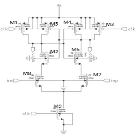
2.2. Conventional Double Tail Dynamic Comparator
Conventional double tail comparator [4] has less stacking compared to the conventional dynamic comparator as shown in fig. 2. In this circuit the double tail enables both a large current in the latching stage and wider tail transistor M1, for fast latching independent of the input common-mode voltage and for low offset a small current in the input stage that means a small M12 transistor.
During reset phase, CLK = 0, tail transistors M1and M12 are off and transistors M8 and M9 pre charge fn and fp nodes to VDD, which in turn causes transistors M6 and M7 to discharge the output nodes to ground.
inverters and also provides a good shielding between input and output. The latch regeneration starts only when one of the nmos transistors M2/M5 is on.
Assuming the case VINP<VINN after the first n-channel transistor of the latch turns on for instance, M5, the corresponding output Outp will be discharged to the ground, leading front p-channel transistor M3 to turn on, charging another output Outp to the supply voltage.
Fig. 2. Conventional double-tail dynamic comparator.
The disadvantage in this comparator is, since fn and fp nodes both discharge to the ground both intermediate stage transistors will be finally cut-off, hence they do not play any role in improving the effective transconductance of the latch stage. In turn, during reset phase, these nodes have to be charged from ground to VDD that means power consumption.
2.3. Modified Double-Tail Dynamic Comparator
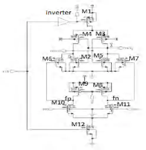
Modified dynamic double-tail comparator [1] schematic diagram is demonstrated in Fig. 3. The modified double tail comparator increases the latch regeneration speed by increasing the input differential voltage. For this purpose, two control transistors M9 and M10 have been added to the first stage in parallel to M8 and M11 transistors but in a cross-coupled manner [Fig. 3(a)].
During reset phase, CLK= 0 and tail transistors M2&M14 are off and M8 & M11transistors pulls both fn and fp nodes to VDD, hence control transistors M9 and M10 are cut off and intermediate stage transistors M6 and M7reset both latch outputs to ground.
During decision-making phase, CLK = VDD and M2&M14 tail transistors are on, transistors M9 and M11 turn off. Furthermore, at the beginning of this phase, the control transistors are still off, since fn and fp nodes are about VDD. Thus, fn and fp start to drop with different rates according to the input voltages. Suppose VINP > VINN, thus fn drops faster than fp, since M13provides more current than M12. The corresponding pMOS control transistor M9turn on due to continue falling of fn and pulling fp node back to the VDD so another control transistor M10 remains off, allowing fn to be discharged completely.
Fig. 3(a). Modified double tail comparator main idea.
Despite the effectiveness of this circuit, when one of the control transistors turns on e.g., M9, a current from VDD is drawn to the ground via input and tail transistor M9, M12, and M14, resulting in static power consumption. In order to overcome this issue, two nMOS switches are used below the input transistors M15 and M16, as shown in Fig. 3(b). At the beginning of the decision making phase, due to the fact that both fn and fp nodes have been pre-charged to VDD during the reset phase, both switches are closed and fn and fp start to drop with different discharging rates. When the comparator detects that one of the fn/fp nodes is discharging faster the control transistors will act in a way to increase their voltage difference. If suppose fp is pulling up to the VDD and fn should be discharged completely, so the switch in the charging path of fp will be opened in order to prevent any current drawn from VDD but the other switch connected to fn will be closed to allow the complete discharge of fn. In other words, the operation of the control transistors with the switches emulates the operation of the latch.
The drawback in this circuit is clk and clkb requires high accuracy timing because the latch stage has to regenerate the differential input voltage coming from input stage at very limited time. Now if we replace the clkb with the inverter whose input is clk signal then clk has to drive heavier load in order to drive largest tail transistor M2 in a smallest possible delay. Now if clkb leads clk, then comparator will undergo increased power dissipation and if clkb lags clk, it results in increased delay means less speed of operation due to short circuit current path from M2 to M6/M7 through M1/M5.
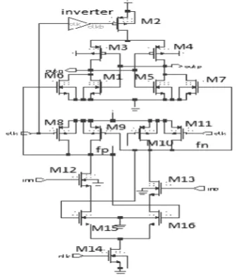
3. Proposed Double Tail Comparator
Due to the better performance of double tail structure in low-voltage applications, the proposed comparator is designed based on the double tail structure. This comparator resolved clock overhead problem by replacing clkb signal with fp and fn nodes.
The circuit is shown in Fig. 4(a). During pre charge(reset) phase clk=0, both PMOS transistors M9 and M10 are turned on and they charge fp and fn nodes capacitances to VDD, which turn on both NMOS transistors M5 and M8 and fp and fn nodes discharge to ground. Sequentially pmos transistors M3, M4 turn off and they make outp and outn nodes to be discharged to ground.
In evaluation (decision) phase clk=VDD, fp and fn node capacitances are discharged from VDD to ground in a different time rate proportion to the magnitude of each input voltage. As a result, an input dependent differential voltage is formed between fp and fn nodes. Once either fp or fn node voltage drops down below a value small enough to turn off M5/M8 the corresponding output nodes will be charged to VDD. If Vinp>Vinn the outp will be high and it is low otherwise.
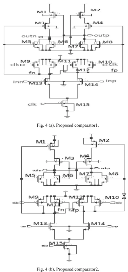
The operation of the circuit shown in Fig. 4(b) is as same as that of Fig. 4(a) but the operation of transistors M1 & M2 in Fig. 4(a) are replaced by M3 and M4 and the operation of M3 & M4 by M1 & M2.
Fig. 4 (a). Proposed comparator1.
Fig. 4 (b). Proposed comparator2.
4. Application
4.1. Flash A/D Converter Design
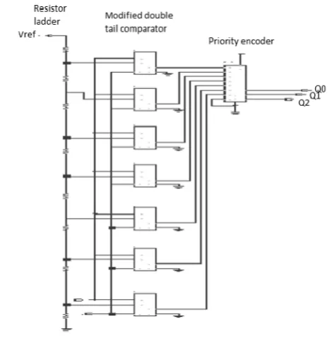
The flash ADC architectures are also called as parallel ADCs, in which the input signal is sampled simultaneously by using multiple comparators to digitalize the analog signal. Due to the parallel architecture it is the fastest ADC among all the other types and is suitable for high bandwidth applications.
Due to presence of 2N resistor it consumes a lot of power, has low resolution. It is mainly used in high frequency applications and in the other types of ADC architectures e.g. multi bit sigma delta and pipelined. Few applications of flash ADCs are satellite communication, radar processing, data acquisition, sampling oscilloscopes, and high-density disk drives. A typical 3-bit flash ADC block diagram is shown in Fig. 5. It can be seen from the figure that 2N-1 comparators are required for “N” bit converter. The resistor ladder network is formed by 2N resistors, which is used to generate the positive reference voltages for each comparator.
Fig. 5: 3bit Flash ADC.
The top and bottom resistors in the resistor string have been chosen to create the 0.5LSB offset in an A/D converter. The reference voltage for each comparator is 1 least significant bit (LSB) less than the reference voltage for the comparator immediately above it. When the input voltage to positive terminal is higher than the reference voltage that is negative terminal voltage of comparator it will generate a "1", otherwise, the comparator output is "0". If the analog input is in between V4 and V5, then the comparators C1 through C4 generates "1"s and all the remaining comparators generate "0"s. The comparators will generate a thermometer code of an input signal. Due to presence of positive feedback, the end state is forced to either a "1" or a "0". A priority encoder is used in the output stage it will provide the three bit digital output for a 3-bit flash A/D converter.
5. Simulation Results
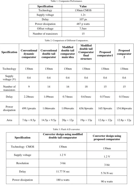
Table 1. Comparator Performance.
Specification Value
Technology 130nm CMOS
Supply voltage 1.2v
Delay 107 ps
Power dissipation 487 p watts
Offset voltage 7.5mv
Number of transistors 15
Table 2. Comparison of Different Comparators.
Specification Conventional dynamic comparator Conventional double tail comparator Modified double tail comparator main idea Modified double tail Comparator final structure Proposed comparator1 Proposed comparator 2
Technology 130nm 130nm 130nm 130nm 130nm 130nm
Supply
voltage (V) 0.6 0.6 0.6 0.6 0.6 0.6
Number of transistors
9 14 16 18 15 15
Delay 2.28nsec 1.09nsec 0.74nsec 0.63nsec 0.57nsec 0.53nsec
Power
dissipation 499.1pwatts 1.06nwatts 1.09nwatts 636.9pwatts 165.9pwatts 154.86pwatts
Area 7.6μ × 8.5μ 14.5μ × 9.5μ 20μ × 12μ 19μ × 13μ 12.6μ × 12μ 12.8μ × 12μ
Table 3: Flash A/D converter.
Specification
Converter design using modified
double tail comparator Converter design using proposed comparator
Technology CMOS 130nm
130nm
Supply voltage 1.2 V
1.2 V
Resolution 3-bit
3-bit
Delay 11.77 N sec
5.76 N sec
Power dissipation 180 u watts
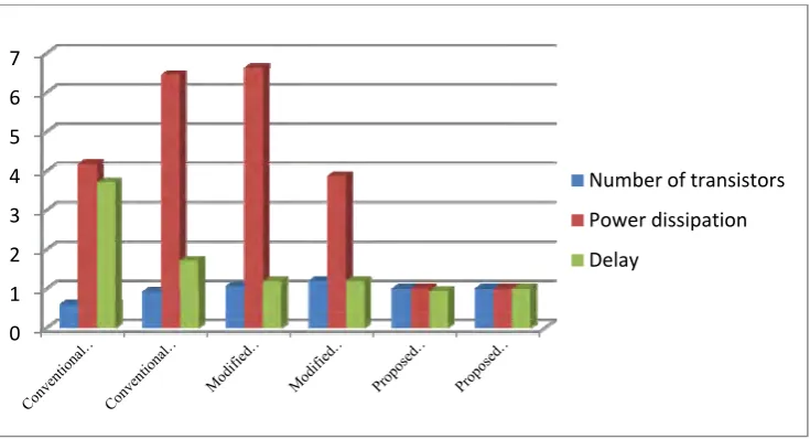
Fig. 6. comparison of different comparators. 6. Conclusion
In this paper, comprehensive delay analysis for clocked dynamic comparators and expressions were presented. Two common structures of conventional dynamic comparator and conventional double-tail dynamic comparators were analyzed. Based on double tail structure a new dynamic comparator with voltage low-power capability was proposed in order to improve the performance of the comparator. Post-layout simulation results in 0.13-μm CMOS technology confirmed that the delay and energy per conversion of the proposed comparator is reduced to a great extent in comparison with the conventional dynamic comparator and double-tail comparator.
References
[1] Babayan-Mashhadi, S.Lotfi, R. “Analysis and Design of a Low-Voltage Low-Power Double-Tail Comparator”, IEEE Transactions on Very Large Scale Integration (VLSI) Systems, Vol: 22 , Issue: 2 ,Page(s): 343 - 352 , feb.2014.
[2] B. Goll and H. Zimmermann, “A comparator with reduced delay time in 65-nm CMOS for supply voltages down to 0.65”, IEEE Trans. Circuits Syst. II, Exp. Briefs, vol. 56, no. 11, pp. 810–814, Nov. 2009.
[3] B. Wicht, T. Nirschl, and D. Schmitt-Landsiedel, “Yield and speed optimization of a latch-type voltage sense amplifier”, IEEE J. Solid-State Circuits, vol. 39, no. 7, pp. 1148–1158, Jul. 2004.
[4] D. Shinkel, E. Mensink, E. Klumperink, E. van Tuijl, and B. Nauta, “A double-tail latch type voltage sense amplifier with 18ps Setup+Hold time”, in Proc. IEEE Int. Solid-State Circuits Conf., Dig. Tech. Papers, Feb. 2007, pp. 314–315.
[5] J. He, S. Zhan, D. Chen, and R. J. Geiger, “Analyses of static and dynamic random offset voltages in dynamic comparators”, IEEE Trans.Circuits Syst. I, Reg. Papers, vol. 56, no. 5, pp. 911–919, May 2009.
[6] P. Nuzzo, F. D. Bernardinis, P. Terreni, and G. Van der Plas, “Noise analysis of regenerative comparators for reconfigurable ADC architectures”, IEEE Trans. Circuits Syst. I, Reg. Papers, vol. 55, no. 6,pp. 1441–1454, Jul.2008.
[7] P. M. Figueiredo and J. C. Vital, “Kickback noise reduction technique for CMOS latched comparators”, IEEE Trans. Circuits Syst. II, Exp.Briefs, vol. 53, no. 7, pp. 541–545, Jul. 2006.
[8] S. Babayan-Mashhadi and R. Lotfi, “An offset cancellation technique for comparators using body-voltage trimming”, Int. J. Analog Integr.Circuits Signal Process., vol. 73, no. 3,pp. 673–682, Dec. 2012.
[9] S. U. Ay, “A sub-1 volt 10-bit supply boosted SAR ADC design instandard CMOS”, Int. J. Analog Integr. Circuits Signal Process., vol. 66,no. 2, pp. 213–221, Feb. 2011.
[10] Y. Okaniwa, H. Tamura, M. Kibune, D. Yamazaki, T.-S. Cheung, J. Ogawa, N. Tzartzanis, W. W. Walker, and T. Kuroda, “A 40Gb/s CMOS clocked comparator with bandwidth modulation technique”, IEEE J. Solid-State Circuits, vol. 40, no. 8, pp. 1680–1687, Aug. 2005.
0 1 2 3 4 5 6 7
Number of transistors
Power dissipation