A NOVEL DESIGN OF REVERSIBLE
SERIAL AND PARALLEL
ADDER/SUBTRACTOR
KRISHNAVENI.D
Engineering Faculty, Department of Electronics and Communication Engineering Sri Bhagwan Mahaveer Jain College Of Engineering, Jain University, Bangalore, Karnataka, India
GEETHA PRIYA.M
Engineering Faculty, Department of Electronics and Communication Engineering Amrita Vishwa Vidhyapeetham, Coimbatore, Tamilnadu, India
Abstract:
Under ideal conditions, Reversible logic gates produce zero power dissipation. So these can be used for low power VLSI design. This paper proposes a new reversible parallel adder/subtractor using 4*4 Reversible DKG gate that can work singly as a reversible full adder and a full subtractor. A serial adder/subtractor is also designed in this paper using Reversible Universal Shift registers and DKG gate. This paper provides a threshold to build more complex arithmetic systems using reversible logic.
Keywords: Low power CMOS; Nanotechnology; quantum computing; Reversible logic circuits.
1. Introduction
Conventional Combinational logic circuits dissipate heat for every bit of information that is lost during their operation. Due to this fact the information once lost cannot be recovered in any way. But the same circuit if it is constructed using the reversible logic gates will allow the recovery of the information. It has been demonstrated that circuits and systems constructed using irreversible logic will result in energy dissipation due to information loss in 1960’s [15]. It is proved that the loss of one bit of information dissipates kT*log2 joules of heat energy, where k is Boltzmann’s constant and T, the absolute temperature at which computation is performed [15]. Zero power dissipation in logic circuits is possible only if a circuit is composed of reversible logic gates [2]. Reversible logic has applications in quantum computing, low power CMOS, nanotechnology, optical computing, and DNA Computing.
A reversible logic gate is an n-input n-output logic device with one-to-one mapping. A gate is considered to be reversible only if for each unique input there is a unique output assignment. This helps to determine the outputs from the inputs and also the inputs can be uniquely recovered back from the outputs provided it is having same number of inputs and outputs. In a reversible gate the outputs are 1’s for exactly half of the inputs. In an n-output reversible gate the n-output vectors are permutation of the numbers 0 to 2n-1. The input that is added to an nxk function to make it reversible is called constant input (CI). The output that is not necessary for further computations is called garbage output (GO). Quantum cost (QC) refers to the cost of the circuit in terms of the cost of a primitive gate. It is calculated knowing the number of primitive reversible logic gates (1*1 or 2*2) required to realize the circuit. [13],[14]. These parameters have to be reduced while designing a reversible circuit. Some of the major problems with reversible logic synthesis are that fanouts cannot be used, and also feedback from gate outputs to inputs is not permitted. However fanout in reversible circuits is achieved using additional gates. A reversible circuit should be designed using minimum number of reversible logic gates. Reversible circuits have been proposed for different purposes like half adder, full adder, multipliers and dividers. Several 4x4 reversible gates (e.g. HNG [8], MKG [9], TSG [10], and PFAG [12]) are designed to work as full adder.
(PG) [12].
2.2. Full adder/subtractor
The existing design for Reversible Full adder/subtractor, ADD/SUB gate [4] is a 4X4 reversible gate which acts as a full adder or a full subtractor when F=0 or F=1 respectively. The number of constant inputs and garbage outputs is 1 and 2 respectively.
2.3. Serial Adder
The serial adder [11] uses shift registers to store the numbers to be added and later stores the sum. A full adder adds bit by bit and the result is stored in a shift register. Each time the sum bit is obtained, the shift register contents are shifted right and the sum bit is stored in the MSB of the shift register. The carry generated after addition is stored in a D Flip-Flop which is later used when the next bits are added. The Fredkin Gate is used in the design of D Flip-Flop and Shift register.
3. 4*4 Reversible DKG Gate
A 4* 4 reversible DKG gate [6] that can work singly as a reversible Full adder and a reversible Full subtractor is shown in Fig 1a. It can be verified that input pattern corresponding to a particular output pattern can be uniquely determined. Its implementation as a full adder and as a full subtractor is shown in Fig 1b and 1c respectively. If input A=0, the proposed gate works as a reversible Full adder, and if input A=1, then it works as a reversible Full subtractor.
It has been proved that a reversible full-adder circuit requires at least two garbage outputs to make the output combinations unique, which is the primary condition for a reversible circuit [1]. The proposed reversible full adder/subtractor circuit produces two garbage outputs, so it is optimal in terms of number of garbage outputs.
Fig 1: Reversible DKG gate [6]
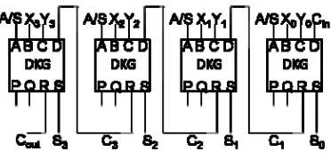
4. Reversible Four Bit Parallel Adder/Subtractor
The binary Full adder/subtractor is capable of handling one bit of each input along with a carry in/borrow in generated as a carry out/ borrow from addition of previous lower order bit position. If two binary numbers each consisting of n bits are to be added or subtracted, then n binary full adders/subtractors are to be cascaded. A Parallel adder/subtractor is an interconnection of full adders/subtractors and inputs are simultaneously applied. The carry/borrow generated at a stage is propagated to the next stage. Thus, delay is more in such type of adders/subtractors.
A 4 bit reversible parallel adder/subtractor is implemented using the reversible DKG gate and shown in Fig 2a. When the control input A=0, the circuit acts as a parallel adder, thus adding two binary numbers of 4 bits each and produces a 4 bit sum and a carry out, as shown in Fig 2b. If the control input A=1, the circuit acts as a parallel subtractor, thus subtracting two binary numbers of 4 bits each and produces a 4 bit difference and a borrow out, as shown in Fig 2c. The same design can be extended to n bits.
Fig 1c: DKG gate implemented as Full subtractor [6]
Fig 2a: Reversible Parallel adder/Subtractor
5. Evaluation of the Proposed Design
A comparison of the full adder/subtractor with the existing circuit [4] is depicted in Table 1. The design of parallel adder/subtractor is compared with the existing design [4] in Table 2.
Table 1: A comparison of proposed reversible full adder/subtractor with the existing circuit
No of Reversible Gates Garbage outputs Constant inputs DKG
Circuit 1 2 1
Existing Circuit 1 [12]
2 3 2 Existing
Circuit 2 [12]
1 2 1
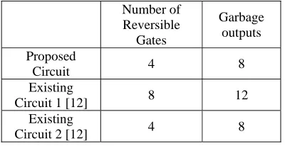
Table 2: A comparison of proposed reversible parallel adder/subtractor with the existing circuit
Number of Reversible Gates Garbage outputs Proposed
Circuit 4 8
Existing
Circuit 1 [12] 8 12
Existing
Circuit 2 [12] 4 8
6. Components used in Serial Adder/Subtractor
6.1. SRK Gate
The 3 X 3 reversible SRK gate [7] can work as a reversible 2:1 Multiplexer as shown in fig 4. When input A is 0, information on input line C is selected and placed on output line R. When input A is 1, information on input line B is selected and placed on output line R. Thus, input line A acts as a select line and input lines C and B act as data input lines; thus forming a 2:1 Multiplexer.
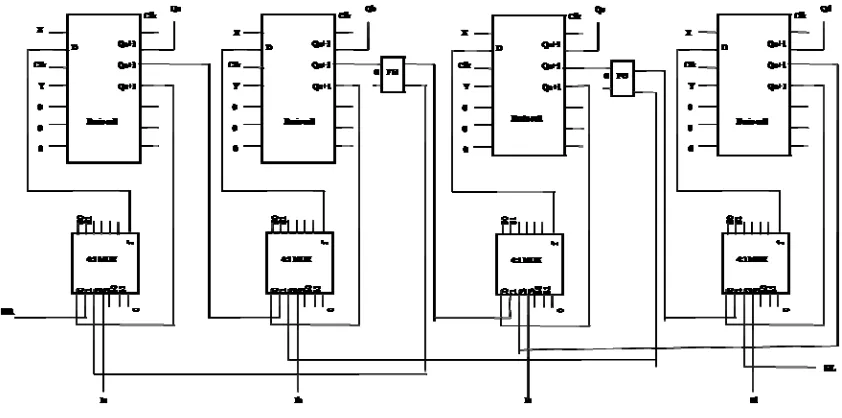
6.2. Universal Shift Register
Shift registers are the registers in which the information can be moved position wise upon the occurrence of a clock signal. The information can be shifted in both the directions in a universal shift register. All modes of operation such as SISO, SIPO, PISO and PIPO can also be performed upon the occurrence of clock. Thus, serial data (SIR during right shift and SIL during left shift) or parallel data (Ia, Ib, Ic, Id) can be loaded into shift register. The values at the select lines determine the operation to be performed as given in Table 3.
Reversible Universal Shift Register (USR) [7] using the basic cell and 4:1 Multiplexers is used in the design of Serial Adder/Subtractor. The block diagram of USR is shown in fig 5.
Table 3: Function table for the reversible universal shift register
S1 S0 Operation 0 0 No Change (Qi) 0 1 Right Shift (Qi-1) 1 0 Left Shift (Qi+1) 1 1 Parallel load (Ii)
The basic cell [7] used in the Design of Reversible Universal Shift Register has a clocked DFF with set/reset input. It makes use of SRK gates and BVF gate to act as a DFF. Asynchronous set/reset implies that the Flip Flop is set or reset irrespective of the input data and clock. The Flip Flop will set, reset or operate as a normal DFF depending on inputs X and Y. When the values of X and Y is 00 or 01, the Flip Flop will reset or set respectively and when XY= 10, it works as a normal DFF.
used to store the carry/borrow generated by the Full Adder/subtractor in the proposed Serial adder/subtractor circuit. D Flip-Flop is shown in the fig 6.
6.4. Control Circuit
The control unit controls the operation of complete Serial Addition or subtraction process by generating control signals and providing them as inputs to various components of the system. Clock signal is given as input to the control circuit. Select lines S1 and S0 to the Universal shift registers are determined from the value of k and Enable signal E. A counter counts the number of shift operations being performed and when the addition or subtraction procedure comes to an end, a signal k=1 is generated which determines the completion of the process.
Clock given to the counter is given by
clk
tff
clk
.
E
. The block diagrams of control circuit and clock generation are showed in fig 7 and fig 8 respectively.Fig 6: DFF using SRK Gate
Fig 7: Block Diagram of circuit generating completion signal k
7. Serial Adder/Subtractor
In the ripple carry adder the delay of carry transfers from one block to the other, results in increase of the total delay of the circuit. Hence serial adder is one of the adders with a delay less than that of the parallel adder. The 4-bit numbers to be added X (augend) and Y (addend) are stored in two Shift registers. When S1S0=01, and the clock is pulsed, SIR is entered into MSB x3 (or y3) as the contents of the register are shifted right one position. The X register serves as the accumulator, and after 4 shifts, the number X is replaced with the sum of X and Y. The addend register is connected as a cyclic shift register, so after 4 shifts it is back to its original state and the number Y is not lost. The serial adder consists of a full adder and a carry FF. At each clock time, one pair of bits is added. When S1S0=01, the positive edge of clock shifts the sum bit into the accumulator, stores the carry bit in the carry FF, and causes the addend register to rotate right.
Initially at time t0, when S1S0=11, the accumulator is loaded with augend X and the addend register is loaded with Y. At this instant the signal E=1. During the next clock pulse, E becomes 0. The carry FF is cleared. Since the Full Adder is a combinational network, the inputs x0 and y0 along with carry 0 are added after a small propagation delay to give the sum sum0 and next carry c1. During the clock pulse t1, the generated sum bit is shifted into the accumulator, and the remaining accumulator digits are shifted right one position. The same shift pulse stores the generated carry in the carry FF and cycles the addend register right one position. The next pair of bits x1 and y1 are now at the full adder input, and the adder generates the sum and the carry. The second clock pulse shifts this sum bit sum1into the accumulator, stores carry c2 in the carry FF and cycles the addend register right. In this way addition of the other 2 bits is performed and stored in accumulator. After 4 clock pulses, t4, the sum of X and Y is in the accumulator, and the addend register is back to its original state.
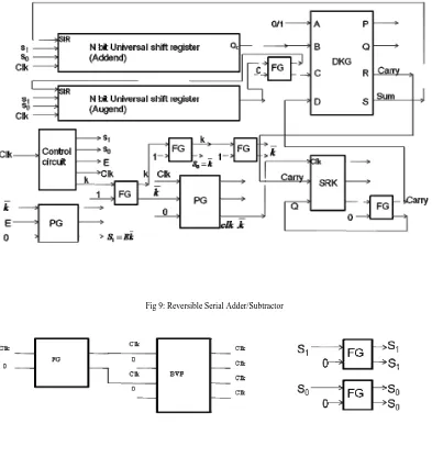
7.1. Reversible Serial Adder/ Subtractor
A Reversible serial adder/subtractor is designed using Reversible DKG gate that acts as an adder or a subtractor when the control signal A/S is ‘0’or ‘1’ respectively. The block diagram and fanout circuits of serial adder are shown in fig 9 and fig 10 respectively.
Two Reversible Universal Shift Registers (USR) are used to store augend /subtrahend (X) and addend /minuend (Y). When select lines S1S0=11 and positive edge of the clock occurs these are loaded with the binary numbers parallel that need to be added or subtracted. After 4 shifts, the number X is replaced with the sum or difference of X and Y in the X register. The addend register Y is connected as a cyclic shift register, so after 4 shifts it is back to its original state and the number Y is not lost. Full adder/subtractor adds the least significant bits of X and Y registers. When S1S0=01, and the clock is pulsed, the sum or difference obtained is shifted into the most significant bit of X register as the contents of the register are shifted right one position. The carry generated is stored in the carry Flip-Flop. At each clock time, one pair of bits is added or subtracted depending on the control bit A/S of the full adder/subtractor. When S1S0=01, the positive edge of clock shifts the sum or difference bit into the X register, stores the carry bit in the carry FF, and causes the addend register Y to rotate right. After 4 clock pulses, the sum or difference of X and Y is in the X register, and the addend register Y is back to its original state.
The control circuit contains a counter which counts the number of shift operations and if 4 shift operations are performed a completion signal k=1 is generated which stops the process and the result is stored.
The select lines given to the USR are determined as
S
1
E
.
k
,
S
0
k
.The clock signal given to the carry Flip-Flop is
clk
FF
clk
.
k
and that to counter isE
clk
clk
counter
.
7.2. Analysis and Results
8. Conclusion
This paper proposes a reversible 4 bit parallel adder/subtractor using 4*4 DKG gates that works singly as a Full adder/subtractor. A new design of Serial adder/Subtractor is proposed using Universal Shift registers and DKG gate. The same design can work as both adder as well as subtractor. The number of reversible gates used and the garbage outputs produced in the proposed design are optimal. The reversible adder/subtractor discussed in this paper can be used to build higher order arithmetic circuits and complex designs of quantum computers. The control circuit can be further elaborately designed in future.
Fig 9: Reversible Serial Adder/Subtractor
References
[1] Ahsan Raja Chowdhury ;Hafiz Md. Hasan Babu; Md. Rafiqul Islam,; Syed Mostahed Ali Chowdhury,“Reversible Logic Synthesis for Minimization of Full Adder Circuit”, Proceedings of the EuroMicro Symposium on Digital System Design(DSD’03), 3-5 September 2003, Belek- Antalya, Turkey,pp-50-54.Journal of Engineering Science and Technology Vol. 2(8), 2010, 3838-3845
[2] Bennett, C. H., “Logical Reversibility of Computation”, IBM J. Research and Development, pp.525-532, November 1973.
[3] Bhagyalakshmi, H.R. ;.Venkatesha, M.K, ‘An improved design of a multiplier using reversible logic gates’, International Journal of Engineering Science and Technology Vol. 2(8), 2010, 3838-3845
[4] Elsayed, A; Layle, A; Maii T. Emam, Reversible Full AdderlSubtractor, 2010 Xlth International Workshop on Syrnbolic and Nurnerical Methods, Modeling and Applications to Circuit Design (SM2ACD)
[5] Feynman R., 1985. Quantum mechanical computers, Optics News, 11: 11-20
[6] Krishnaveni,D, Geetha Priya,M, “Design of an Efficient Reversible 8x8 Wallace Tree Multiplier”, Submitted for Review to Circuits and Systems-I Journal, IEEE
[7] Krishnaveni,D, Geetha Priya,M, “A Novel Design of Reversible Universal Shift Register with Reduced Delay and Quantum Cost”, Submitted for Review to VLSI Systems Journal, IEEE
[8] Haghparast, M ; Navi, K, "Design of a novel reversible multiplier circuit using HNG gate in nanotechnology", Am. 1. Applied Sciences, 5 (2008) 282
[9] Haghparast, M ; Navi, K ; Shams, M, "Novel reversible multiplier circuit in nanotechnology", World App!. Sci. 1., 3 (2008) 806. [10] Himanshu Thapliyal ; Srinivas, M.B, ”Novel Reversible ‘TSG’ Gate and Its Application for Designing Components of Primitive
Reversible/Quantum ALU”
[11] Himanshu Thapliyal ; Srinivas, M.B,” An Extension to DNA Based Fredkin Gate Circuits: Design of Reversible Sequential Circuits using Fredkin Gates”
[12] Islam, M.S. et a!.,"Low cost quantum realization of reversible multiplier circuit", Information technology journal,8(2009)208 [13] Kerntopf,P; Khan, M.H.A.; Perkowski, M.A, 2004. On universality of general reversible multiple valued logic gates, IEEE proceeding
of the 34th international symposium on multiple valued logic (ISMVL’04), pp: 68‐73.
[14] Kerntopf, P ; Perkowski, M, 2001.Reversible Logic. Invited tutorial, Proc.EURO‐MICRO, Sept 2001, Warsaw, Poland