22 & 23.04.2017
In association with
InternationalJournal
of
ScientificResearch inScience andTechnologyDesign of CMOS 8-Bit Parallel Adder Energy Efficient
Structure using SR-CPL Logic Style
Aravinth.T.S
1, Sundar.R
2, Felix Muthu
3 1Assistant Professor, 2Assistant Professor, 3PG Scholar 1,3 Department of Electronics & Communication Engineering,
2
Department of Electrical & Electronics Engineering
1,3Karpagam Academy of Higher Education (Deemed to be University), Coimbatore, Tamil Nadu, India 2Karpagam College of Engineering, Coimbatore, Tamil Nadu, India
ABSTRACT
We present high speed and low power 8-Bit parallel adder cells designed with modified SR-CPL logic styles that had a reduced power delay product (PDP) as compared to the previous logics DPL and pass transistor logic. We have carried out a comparison against other parallel adders reported as having a low PDP, in terms of speed and power consumption. All the parallel adders were designed with a 0.18µm CMOS technology virtuoso cadence environment. Simulations of the circuit show that the proposed parallel adders have reduced the power from 0.33mW to 0.24mW.
Keywords : SR-CPL logic Styles, PDP, DPL, Pass Transistor, Logic, Virtuoso Cadence Environment.
I.
INTRODUCTION
Energy effectiveness is one of the most required features for modern low power electronic devices , which have
been designed for high-performance portable
applications. In one hand, the ever increasing market segment of portable electronic devices demands the availability of low-power building blocks that enable the implementation of long-lasting battery-operated systems. On the other hand, the general trend of increasing operating frequencies and circuit complexity, in order to cope with the throughput needed in modern high-performance processing applications, requires the design of very high-speed circuits. The power-delay product (PDP) metric relates the amount of energy spent during
the realization of a determined task, and stands as the more fair performance metric when comparing optimizations of a module designed and tested using different technologies, operating frequencies, and scenarios. Addition is a fundamental arithmetic operation that is broadly used in many VLSI systems, such as applicationspecific digital signal processing (DSP) architectures and microprocessors. This module is the
core of many arithmetic operations such as
addition/subtraction, multiplication, division and address generation. As stated above, the PDP exhibited by the Parallel-adder would affect the system’s overall performance
. Thus, taking this fact into consideration, the design of a Parallel adder having low-power consumption and low propagation delay results of great interest for the implementation of modern digital systems. In this paper, we report the design and performance comparison of Parallel-adder cells implemented with an alternative internal logic structure, based on the multiplexing of the Boolean functions XOR/XNOR and AND/OR, to obtain balanced delays in SUM and CARRY outputs, respectively, and SR-CPL logic styles, in order to
explains the features of the simulation environment used for the comparison carried out to obtain the power and speed performance of the Parallel-adders. Section V reviews the results obtained from the simulations, and Section VI concludes this work.
II.
Literature Review
Recursive Approach to the Design of Parallel Self-Timed Adder
It proposes to use a zero-delay overhead self-timed pipeline style that supports very high speed operation. Developed techniques to enable the application of zero delay-overhead self-timed pipeline in this context and realize run-time pipeline depth control. Simulations under variable data rate scenarios demonstrate a significant performance gain [1].
CMOS Full Adder for Energy Efficient Arithmetic Applications
The design of high-speed low-power full adder cells based upon an alternative logic approach has been presented. Which results in a great improvement on regards of power-delay metric for the proposed adders, when compared with several previously published realizations [2].
Area Efficient Self Timed Adders for Low Power Applications in VLSI - The parallel asynchronous self-timed adder circuit is efficiently described using a handshaking protocol and also compared with other
adders proposed adders. The MAC unit is
implemented and the process is achieved efficiently. Simulation results demonstrate the effectiveness of the proposed framework in parallel prefix adder using multiplication through addition process [3].
Design of Low Power Asynchronous Parallel Adder - This paper describes an asynchronous parallel adder. It is based on Radix method for faster computation of sum and to reduce delay caused by carry chain. The computation has been carried out using parallel process. The aim of this work is to reduce the Power Delay Product (PDP) and Energy Delay Product (EDP) of an adder [3].
Self-Repetitive Approach to the Design of a Parallel
Self- Timed Adder - This brief presents a parallel single-rail self-timed adder. It is based on a recursive formulation for performing multi bit binary addition. The operation is parallel for those bits that do not need any carry chain propagation [4].
Design of a Parallel Self-Timed Adder Using Recursive Approach - This brief presents a parallel single-rail self-timed adder. It is based on a recursive formulation for performing multibit binary addition. The operation is parallel for those bits that do not need any carry chain propagation. Thus, the design attains logarithmic per- formance over random operand conditions without any special speedup circuitry or look-ahead schema [5].
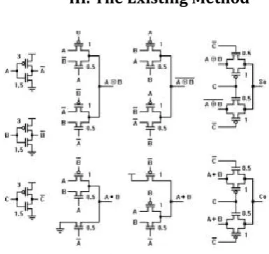
III.
The Existing Method
Figure 1 Existing Circuitary
Figure 2 Completion Detection Circuit
module. The internal logic structure has been adopted as the standard configuration in most of the enhancements developed for the 1-bit full-adder module. In this configuration, the adder module is formed by three main logical blocks: a XOR-XNOR gate and XOR blocks or multiplexers to obtain the SUM (So) and CARRY (Co) outputs. The major problem regarding the propagation delay for full-adder built with the logic structure is that it is necessary to obtain an intermediate .8_signal and its complement, which are then used to drive other blocks to generate the final outputs. Thus, the overall propagation delay and, in most of the cases, the power consumption of the full-adder depend on the delay and voltage swing of the .8_signal and its complement generated within the cell. So, to increase the operational speed of the full-adder, it is necessary to develop a new logic structure that does not require the generation of intermediate signals to control the selection or transmission of other signals located on the critical path.
IV.
The Proposed Method
In this method report there are not signals generated internally that control the selection of the output multiplexers. Instead, the input signal, exhibiting a full voltage swing and no extra delay, is used to drive the multiplexers, reducing so the overall propagation delays. The capacitive load for the input has been reduced, as it is connected only to some transistor gates and no longer to some drain or source terminals, where the diffusion capacitance is becoming very large for sub-micrometer technologies. Thus, the overall delay for larger modules where the signal falls on the critical path can be reduced. The propagation delay for the So and Co outputs can be tuned up individually by adjusting the XOR/XNOR and the AND/OR gates; this feature is advantageous for applications where the skew between arriving signals is critical for a proper operation and for having well balanced propagation delays at the outputs to reduce the chance of glitches in cascaded applications. The inclusion of buffers at the full-adder outputs can be implemented by interchanging the XOR/XNOR signals, and the AND/OR gates to NAND/NOR gates at the input of the multiplexers, improving in this way the performance for load-sensitive applications.
Figure 3 SR-CPL Logic Style
V.
Energy Efficient Parallel Full Adder
After studying the truth table of full adder in Table 1, it can be observed that the So output is equal to the (A XOR B) value when C=0, and equal to (A XNOR B) when C=1. From this observation we conclude that a multiplexer will be used to obtain the respective value based upon the Carry input, as stated earlier. Using the same scenario, the Co output is equal to the (A AND B) value when C=0, and (A OR B) value when C=1. In the similar way, carry will be used to drive a multiplexer. Hence, an energy efficient logic scheme to design a full adder cell can be formed by a logic block to get the (AXOR B) and (AXOR B) signals, other block to obtain (A AND B) and (A OR B) signals, and two multiplexers being driven by the Carry input to generate the So and Co outputs, as shown in Figure 2.
Figure 4. Proposed Parallel Half Adder using SR-CPL
VI.
Results
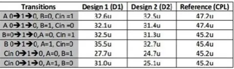
Table 2 Delay
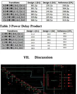
Table 3 Power Delay Product
VII.
Discussion
Figure 5. 8-Bit Parallel Full Adder using SR-CPL
Two new designs based on SR-CPL and DPL style full adders are being examined in this project. The main advantages of this design are: Multiplexers are directly controlled by Cin instead of internally generated signals thereby reducing delay.
Capacitive load on Cin is reduced.
Figure 6 Output Plot of Proposed Circuitry
The propagation delay of So and Co can be tuned by sizing XOR/XNOR gates appropriately. The inclusion of buffer at input can be integrated by using NAND/NOR gates instead of XOR/XNOR gates. Buffers are placed at the inputs are placed to account for the load the
device offers at the inputs.
Also, since the designs presented here consist of pass transistor logic which has no direct power supply connection, the power consumed by the device also comes through these inverters. The output inverters account for the power due to degraded voltage swing and slopes of full adder output. The full adders have been simulated using 180-nm CMOS technology using cadence virtuoso. The value of supply voltage VDD used was 1.8V.
Figure 7 Power Delay Plot for SR-CPL vs Existing Styles
Figure 8 Power Dissipation Plot for SR-CPL vs Existing Styles
VIII.
Conclusion
We have presented SR-CPL parallel full adder and CPL style adder. The key features observed were: 1. the proposed designs reduce both total average power and worst case delay of the circuit. Total average power reduction of about 30-38% is observed for D1 and about 27-45% for D2 2. Delay of D1 is comparable to that of the CPL logic (it is slightly greater for most transitions). Delay of D2 is significantly smaller as compared to the reference CPL Design – from about 16% to 31% 3. The overall Power delay product of both the designs is reduced as compared to the standard CPL design ranging from about 5% to 25% for D1 and about 43% to 66% for D2 4. The designs are more efficient both power wise and delay wise as compared to the standard CPL design used 5. The transistor count for the proposed designs is also much less as compared to the s CPL adder (26 & 28 as compared to 38) 6. The proposed designs occupy much less area as compared to the CPL adder (116 μm2 & 118 μm2 for D1 and D2 vs 238 μm2 for CPL adder)
IX.
References
[1] A. M. Shams and M. Bayoumi, "Performance evaluation of 1-bit CMOS adder cells ", IEEE ISCAS, Orlando, Florida, May 1999, pp. I27 -130. [2] A.P.Chandrakasan, S.Sheng and R.W.Brodersen, "Lowpower CMOS digital design ", IEEE JSSC, Vol. 27, April 1992, pp. 473-483.
[3] N. Weste and K. Eshraghian, Principles of CMOS design, A system perspective, Addison-Wesley, 1988. 4K. M. Chu and D. Pulfrey, "A comparison of CMOS circuit techniques: Differential cascode voltage switch logic versus conventional logic, "IEEE J. Solid-State Circuits, vol. SC-22, no. 4, pp.528-532, Aug.1987.
[4] K. Yano, K. Yano, T. Yamanaka, T. Nishida, M. Saito, K. Shimohigashi, and A. Shimizu, "A 3.8 ns CMOS 16-b multiplier using complementary pass-transistor logic," IEEE J. Solid-State Circuits, vol. 25, no. 2, pp. 388-395, Apr. 1990.
[5] M. Suzuki, M. Suzuki, N. Ohkubo, T. Shinbo, T. Yamanaka, A. Shimizu, K. Sasaki, and Y. Nakagome, "A 1.5 ns 32-b CMOS ALU in double pass-transistor logic," IEEE J. Solid-State Circuits, vol. 28, no. 11, pp. 1145-1150, Nov.1993.
[6] R. Zimmerman and W. Fichtner, "Low-power logic styles: CMOS Versus pass-transistor logic," IEEE J. Solid-State Circuits, vol. 32, no. 7, pp. 1079-1090, Jul. 1997.
[7] N. Zhuang and H. Wu, "A new design ofthe CMOSfull adder", IEEE JSSC, Vol. 27, No. 5, May 1992, pp. 840-844
[8] A. M. Shams and M. Bayoumi, "A new cellfor low power adders ", Proceedings of the International MWSCAS, 1995.
[9] C. Chang, J. Gu, and M. Zhang, "A reviewof 0.18-full adder performances for tree structured arithmetic circuits," IEEE Trans. Very Large Scale Integr. (VLSI) Syst., vol. 13, no. 6, pp. 686-695, Jun. 2005.
[10] M. Aguirre and M. Linares, "An alternative logic approach to implement high-speed low-power full adder cells," in Proc. SBCCI, Florianopolis, Brazil, Sep. 2005, pp.166-171.
[11] Reto Zimmermann and Wolfgang Fichtner,
Fellow, IEEE" Low-Power Logic Styles: CMOS Versus Pass- Transistor Logic" in IEEE Journal Of Solid-State Circuits, Vol. 32, No. 7, July 1997.
[12] Aguirre-Hernandez, Mariano, and Monico
Linares- Aranda. "CMOS fulladders for energy-efficient arithmetic applications." Very Large
Scale Integration (VLSI) Systems, IEEE
Transactions on 19.4 (2011): 718-721.
[13] Quintana, J. M., et al. "Low-power logic styles for full- adder circuits."Electronics, Circuits and Systems, 2001. ICECS 2001. The 8th IEEE International Conference on. Vol.3. IEEE, 2001 [14] J Rabaey, A Chandrakasan, and B Nikolic, Digital