Exploiting the Reconfigurability of
Programmable Hardware for Neural Engineering
Arfan Ghani
University of Bolton, Bolton, England, United Kingdom Email: [email protected]
Abstract—The use of programmable devices leads to flexible and area-efficient implementation of biologically plausible neural entities such as synapses and neurons. However, the area constraints of reconfigurable devices such as the Field Programmable Gate Arrays (FPGAs) limit their use to rather small and already trained neural networks. This paper investigates and describes area-efficient spiking neural building blocks to implement integrate-and-fire (IF) and leaky integrate-and-fire (LIF) neuron models on reconfigurable hardware. It is demonstrated that an abstract behaviour of spiking neurons can be emulated for bit accurate implementation. In a linear comparison, 2×10³ synapses and 1.2×10³ fully parallel artificial spiking neurons can be implemented with the proposed building blocks and architectures. By using bigger devices with more logic elements such as Virtex-5, it is possible to fit almost 4.3×10³ synapses and 2.5×10³ neurons. The main contributions of this paper include area-efficient fully parallel architectures that exclude the use of embedded multipliers, area-efficient architecture for a leaky membrane, and compact implementation of neural cell which can be used for emulating large scale fully parallel spiking neural networks.
Index Terms—neural engineering, reconfigurable neural architectures, neuromorphic hardware
I. INTRODUCTION
Inspired by the way the human brain processes information, scientists have been researching neural networks (NNs) since the early 1940s [1]. Neural Networks (NNs) are information processing paradigm inspired by the way mammalian nervous systems process information. The key element of this paradigm is the structure of the information processing system which is composed of a large number of highly interconnected processing elements, neurons, working in parallel to solve a specific problem.
The neuron is made up of four main parts; dendrites, synapses, axon and the cell body. It is known that a neuron is essentially a system that accepts electrical currents which arrive on its dendrites. It sums these and if they exceed a certain threshold it generates a new pulse which propagates along an axon. The information is transmitted from an axon to a dendrite via a synapse by means of diffusing chemical neurotransmitters across the synaptic cleft.
Manuscript received April 21, 2014; revised December 10, 2014.
implementation of spiking neuron models. An appropriate time-efficient and bit-accurate design flow for spiking neural network implementation is devised and area-efficient building blocks for integrate-and-fire (IF) and leaky integrate-and-fire (LIF) neuron models were investigated. The contents of this paper are organised as follows:
Section II discusses neuron models chosen for this research and Section III details the IF and LIF reconfigurable architectures and synaptic membrane modelling. Finally, a discussion of the performance obtained, limitations, paper findings and possible areas of improvement are concluded in Section IV.
II. HARDWARE MODELLING OF SPIKING NEURONS
In contrast to classical neural networks, biological neurons process their information through short pulses, called spikes. A spike is transmitted through an axon which connects with other neurons through dendrites. Ideally, each spike contributes to the membrane potential by accumulating corresponding post synaptic potential. Broadly speaking, if an incoming spike leads to an increase in the membrane potential then it is called an EPSP (Excitatory Post Synaptic Potential) otherwise it is called an IPSP (Inhibitory Post Synaptic Potential). Once the neuron has fired, it resets its membrane potential. This process continues and all neurons in the network keep communicating with other neighbouring neurons. The best known and the most biologically plausible model is the Hodgkin-Huxley (HH) model [7]. However, there are other phenomenological and less realistic models which can demonstrate most of the characteristics presented in the HH neurons such as Izhikevich, Spike Response Model (SRM) and IF models. The most biologically plausible models are not well suited for hardware implementation as they are expensive in terms of computational resources. Therefore, other simplified models such as and-fire (IF) or leaky integrate-and-fire (LIF) [5], [6] are more frequently used for hardware implementations. Software implementations are useful for investigating the capabilities of different models and their applicability but they are not adequate for real time processing or fully parallel large scale network implementations.
A. Neuron Models
The behaviour of high dimensional models such as HH is relatively more difficult to analyse, therefore reduction of the four dimensional equations of the HH model to one dimensional is highly desirable for efficient implementation purposes. The neuron models chosen for this investigation are the IF and LIF. These models are chosen because of their simplicity, tractability and biological plausibility in comparison with detailed compartmental models such as Hodgkin-Huxley. It is important to have a neural model which is fast, less complex, fully parallel and numerically accurate. All integrate-and-fire neurons can be stimulated either by external input current or the inputs received from different presynaptic neurons.
Mathematically, the IF model can be expressed as:
𝐼(𝑡) = 𝐶𝑚𝑑𝑢𝑑𝑡𝑖 (1)
where Cm is the membrane capacitance, ui(t) is the membrane potential, and I(t) is the input current. This model is less biologically plausible because real neurons do not respond instantaneously to their input stimuli. The perfect IF neuron model does not take into account the leakage current which is a time constant characteristic for charging and discharging of the membrane potential.
In contrast to the perfect IF, the basic circuit of a LIF model consists of a resistor in parallel with a capacitor driven by an external current I(t). According to this model, total current is divided into two components and 3 described by (2), (3) and (4).
𝐼(𝑡) = 𝐼𝑅+ 𝐼𝐶 (2)
𝐼(𝑡) =𝑢𝑚(𝑡)
𝑅𝑚 + 𝐶𝑚
𝑑𝑢𝑚
𝑑𝑡 (3) 𝜏𝑚𝑑𝑢𝑑𝑡𝑚= −𝑢𝑚+ 𝑅𝑚𝐼(𝑡) (4)
where um is the membrane potential and τm is the membrane time constant of the neuron. The membrane potential resets to a ‘reset’ value once the neuron has fired.
implementations on FPGAs are to some extent unconventional as FPGAs were not originally developed with this in mind. Therefore it is important to adopt a design flow which can support the complexity in translating SNNs onto FPGAs and lead to optimised area/time-efficient implementations.
Simulink is a well-known tool for high level modelling and can be interfaced with the Xilinx System Generator (XSG) toolbox. This can provide an integrated environment where an algorithm can be tested in MATLAB and modelled for hardware implementation. XSG provides a library of hardware blocks that can be converted into hardware description languages for synthesis and bit streams can be generated to map onto target FPGA devices. Blocks with less complexity such as multiplexers, gates and registers are directly converted into VHDL while blocks such as multipliers and memories are supported through Xilinx CORE Generator. XSG design flow is used for the experiments in this paper because tool support is available from algorithm development to the hardware implementation. The hardware models can be synthesised and implemented on target FPGAs through the ISE design suite. It is particularly beneficial because most of the neural simulators can be used within the MATLAB environment and their functionality can be verified. The design flow is time-efficient and a bit and cycle accurate design can be implemented on reconfigurable platforms.
III. RECONFIGURABLE MULTIPLIERS-LESS
ARCHITECTURES
The proposed hardware architectures are motivated by the dynamics involved in the cortical spiking neurons. There are numerous studies about spike activity in cortical neurons and detailed discussion about them is out of the scope of this paper, the reader is referred to [19] for further insight. It has been observed that neurons activity in the cortex is highly stochastic due to the random synaptic transmission delays. These delays vary from synapse to synapse. Both synaptic delays and synaptic efficacies can be either fixed or variable based on the network activity. The inclusion of randomness in neural dynamics is an acceptance to the fact that very little is known about how neurons in the cortex interact with rest of the brain and outside world. The whole system might have considered deterministic if all these been known.
Another possible reason for stochastic behaviour in neurons may be due to thermal and network noise. This occurs due to signal transmission and network effects [19], [20]. Biologists are still trying to find out the exact mechanisms behind these apparent stochastic behaviours in cortical neurons which are so reliable and fault tolerant. Since the cerebral cortex typically contains a very large number (20 billion) of neurons, the probability of a neuron failure in the network is high and it may be due to the distributed nature of neurons that tends to make them immune to faults. Inspired by these studies, simple and area efficient multiplier-less architectures were developed to model some of the characteristics of spiking neurons in the cortex.
In spike based models such as IF or LIF, neural operations can be performed with basic logic gates and streams of input pulses. Multiplication is one of the most common and critical operations in many computational systems and is one of the bottlenecks for the implementation of large scale biologically plausible neural networks. In hardware, a traditional multiplier unit is extremely expensive in terms of logic utilisation and inefficient in terms of power consumption. Low cost FPGA devices don’t have dedicated multiplier units on chip while high end FPGA devices have limited numbers of dedicated multipliers, which are significantly less than the number of neurons that can be implemented. If a single synapse with a traditional 8 bit multiplier and 12 bits resolution is to be implemented on a Virtex-II Pro FPGA (xc2vp50) then almost 26 slices and one embedded multiplier will be required. Since the total number of embedded multipliers available on this device is 232, the maximum number of synapses will be restricted to the maximum number of embedded multipliers. In the case of large networks, available logic has to be utilised for implementing multipliers which significantly restricts the maximum number of synapses and neurons that can be implemented on a given device.
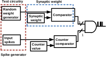
The proposed approach to the area optimised multiplier-less spiking neuron cell uses a scheme where synaptic multipliers are replaced with pulse density. The weight value for each synaptic connection can be modified; in this case where learning is considered to be off line, the weight values were fixed. A random synapse activity can be generated with area efficient logical and arithmetic operators. A chain of adders are used in order to add incoming synaptic values for the membrane potential.
Random weight generator
Input spikes
Synaptic weight
Counter value
Comparator
Counter comparator Synaptic weight
1
1
Spike generator Test circuitry
Figure 1. Synapse architecture
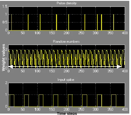
generated at each time step and therefore, a large weight results in many pulses and a small weight results in very few pulses (see Fig. 2 and Fig. 3). In other words, the weights in this architecture are represented by pulse density. The output pulses generated through the synapse block are accumulated in the membrane potential.
The LFSR block introduces randomness in the synapse which is one of the important features of neuronal activity observed in the cortical neurons. This is very flexible in terms of the spike counts where both single or spike bursts can be modelled. In these simulations, single spikes were counted. The neuron’s membrane is modelled with a simple accumulator with 12 bit resolution and threshold logic. An output spike is generated if the synaptic potential exceeded a threshold value and this spike is then transmitted to other neurons in the network.
Time steps
W
e
ig
h
t
v
a
lu
e
s
Figure 2. Pulse density in terms of output spikes corresponding to the weight value (0.1).
Time steps
W
e
ig
h
t
v
a
lu
e
s
Figure 3. Pulse density increases with an increased weight value (0.4) shown with “white arrow” in middle plot.
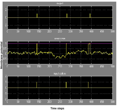
The proposed architectures are composed of two sub units – a synapse and neuron. The synapse model was shown in Fig. 1 and the neuron model is shown in Fig. 4. Hardware simulations are shown in Fig. 5. As shown in Fig. 4, the synapses are added in the synaptic adder block where input spikes coming from other neurons in the network are processed through the synapse block and added in the synaptic adder block.
The synaptic efficacy of each spike is accumulated in the membrane potential.
A random noise is also included in the membrane potential and the total membrane potential is compared with the membrane threshold. An output spike is generated if the membrane potential exceeds a certain threshold and the membrane potential resets to the reset voltage. The simulation results are in very good agreement with the theory reported in [6], [21], [22].
+
>=
OutputSynapse 0
Random weight
generator Synaptic
weight
Comparator
Counter comparator Synaptic weight
1
1
Counter value Input spike
Synaptic adder
Noise inclusion and membrane potential accumulation
+
Accumulatorrst
Membrane threshold comparator
Membrane
In
p
u
t
s
p
ik
e
s
I0
I1
In
Synapse 1
Synapse n Vth
Figure 5. Neuron membrane and integration of potential with single synapse (membrane threshold = 1, fixed time step = 0.125ms, band
limited white noise, σ = 0.01).
Since multipliers are one of the area consuming operators therefore considerable amount of logic can be saved. There is no straight forward way to quantify utilisation of hardware resources for different logic blocks because it depends on the precision of the arithmetic operators, input bit-widths, synthesis tool optimisation, designer’s skills and appropriate design flows. In order to analyse the area utilisation of a multiplier on a Virtex-II Pro (xc2vp50) FPGA, different implementations were performed with multiple bit resolutions and bit-widths.
The breakdown of these implementations is shown in Table I. It can be seen that the logic utilisation increases with an increased bit resolution and bit-width, however there are other factors which also contribute to the area utilisation on a target FPGA. In a top down strategy, it is very important that an optimised architecture is developed. Another limiting factor is the maximum number of local and global connection lines available on a target FPGA. This can severely limit the routing resources and despite the availability of logic, the synthesis tool may not be able to fit the design. The proposed architectures overcome the burden of synaptic multipliers and a significant improvement can be achieved in terms of the maximum size of a network that can be implemented.
TABLEI. AREA UTILISATION OF TWO INPUTS MULTIPLIER WITH
DIFFERENT BIT-WIDTHS AND BIT RESOLUTIONS Two inputs
(Bit-width)
Bit resolution Logic utilisation
Slices LUTs 2×2 4 8 9
16 11 14 28 14 16 8×8 8 20 35 20 41 76 32 50 82 14×14 9 31 45 21 106 184 33 127 225
The motivation behind this investigation was to map extremely compact neural cells in the order to allow large numbers of neurons to be fully parallel on a single FPGA device. A scalable design strategy is proposed and resources are calculated. The overall area of hardware resources solely depends on the dynamics involved in the model. This architecture is flexible and can easily accommodate more precise characteristics of biological neurons such as axonal delays. The architecture is modified for including axonal delays, where a delay is introduced with a chain of registers and selected through a multiplexer as shown in Fig. 6.
Once the neuron has fired, the intermediate register is triggered with the reset signal to drop the membrane potential to the reset level. The axonal delay can be selected through concatenation and multiplexer block accordingly. A spike will be transmitted without any delay if the input values of a ‘concat’ block are selected as ‘00’, and if other values are used such as ‘01’, ‘10’ and ‘11’ then the spike will be transmitted after multiple register delays. The values of register delays can also be changed and all other values are reconfigurable and can be adjusted accordingly.
M
e
m
b
ra
n
e
White noise Concat Sel A
B
reg reg reg
Mux rst
Reg
Output Axonal delay
S
y
n
a
p
s
e
s
I0
I1
In
>=
Vth
Comparator
Figure 6. Axonal delay architecture
A Virtex II Pro device xc2vp50 is used for implementation and resources are calculated. The device has a maximum of 53,136 logic cells or 23,616 slices. In a linear comparison, almost 2×10³ synapses and 1.2×10³ neurons can be implemented with the proposed architecture. By using a state-of-the-art device such as the Virtex-5, which has 331,775 logic cells or 51,840 slices, it is possible to fit almost 4.3×10³ synapses and 2.5×10³ fully parallel neurons at the same time. Maximum frequency and logic utilisation strongly depends on the network size and numerical precision. These numbers (synapses and neurons) are indicative; however the total number of neurons that could be implemented on a target device depends on the synthesis tool and the architecture of a target device. The local and global lines significantly affect the routing of the design and after 80% of the device utilisation it becomes very hard for the synthesis tool to fit logic in a linear scale.
Logic utilisation for a single synapse and neuron for the proposed architecture is shown in Table II and resource estimation for different network sizes is shown in Table III. As shown in Table III, higher bit resolution costs more slices and it is important to keep the balance between desired functionality and minimum bit resolution. It is also shown that the maximum speed of a design depends on the architecture and the size of a network. A compact and carefully optimised design will have higher speed in comparison to a bigger design where routing
Time steps
M
e
m
b
ra
n
e
p
o
te
n
ti
a
delays slow down the maximum speed that can be achieved.
TABLE II. RESOURCE ESTIMATION FOR ONE NEURON AND ONE
SYNAPSE (POST PLACE AND ROUTE) Synapses Neuron Total Max
Frequency (MHz)
Embedded Multipliers
Bit resolution
% usage (xc2vp50)
Slices Bit
resolution Slices Bit
resolution Slices
4 6 8 10 16 178 4 6 TABLEIII. RESOURCE ESTIMATION OF MULTIPLIER-LESS
IMPLEMENTATION (POST PLACE AND ROUTE) Neuron:
Synapse Bit Resolution N:S
Slices (XST post place and route)
Embedded Multipliers
Frequency (MHz) 1:1 8:4 16 0 178 1:3 12:10 78 0 94 1:10 12:12 143 0 94
The proposed architecture is promising in terms of logic utilisation and compares well to the existing approaches. For example, Upegui, et al. [9] reported that without learning, one neuron and a synapse can be implemented on a Spartan II sc2s200 device with 23 slices, and with learning it takes 41 slices. In order to observe the scalability of the neuron model, different topologies were also investigated. Maya, et al. [12] reported that 13 slices are required for a single synapse implementation on Virtex XV50-6 and 47 slices for the summing module. The maximum operating frequency achieved with this design was 90MHz. An XOR problem was compiled for the same device with maximum frequency of 90MHz and it took 240 slices. Schrauwen, et al. [23] implemented spiking neurons with serial arithmetic on a Spartan SC3S200 device. It is reported that with 12 bit resolution, one synapse model and 10 inputs can be implemented with a maximum clock speed of 120MHz. The total number of neurons that could be implemented was limited to 56. In another study, Xicotencatl, et al. [24] demonstrated that 1000 synapses and 1120 somas (neurons) can be implemented on an XCV2000 device with 97% resource utilisation.
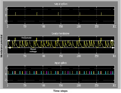
In order to further include the biological characteristics of leakage membrane, a modified architecture is proposed with the leaky membrane as shown in Fig. 7 where input spikes were accumulated and an output spike is generated when the membrane potential exceeds a certain threshold. The output spike is delayed with the chain of registers which models the axonal delay and a reconfigurable value can be selected with the select input of the multiplexer block. The membrane potential resets to the reset value soon after the firing and in the absence of input spikes the membrane potential decays exponentially towards resting potential. It takes only 58 slices to implement one synapse and one LIF neuron with axonal delay circuit. Different biological properties can be modelled and incorporated in the proposed extended architecture including different membrane decays, temporal integration, and axonal delays. All parameters are programmable such as axonal delay, membrane noise and threshold value. These parameters can be adjusted accordingly.
Membrane dynamics play an important role in modelling long and short term memory. Different values of decay constants determine the duration of memory held in network nodes; a larger decay constant means a sharp decay, hence a shorter memory. A smaller decay constant means a slower decay, hence a longer memory. Using the proposed architectures, most of the biological properties such as spatio-temporal spike integration, firing threshold, resting value and leaky membrane can be emulated on reconfigurable hardware. Hardware simulations with the leaky membrane are shown in Fig. 8.
s
y
n
a
p
s
e
s
M
e
m
b
ra
n
e
White noise Sel
reg reg reg
Mux
Concat
A B
>=
Vth
Comparator
Reg
rst
Output
Synapses Soma Axonal delay
I0
I1
In
Figure 7. Modified architecture with leaky membrane
M
e
m
b
ra
n
e
p
o
te
n
ti
a
l
Reset voltage Threshold
Time steps
Figure 8. Three different input spikes accumulation and output spike generation
IV. DISCUSSION/CONCLUSION
Both IF and LIF models are spiking neuron models. In a perfect integrator, the exact timing of spikes is less important because the membrane has no leaky effect; however, in the LIF model the exact timing of spikes does play an important role and a neuron firing time can change if presynaptic spikes are received simultaneously. The shape of different input spikes is not important and contains no information bearing significance. It is the time between spike events which is used to convey information.
is flexible requiring minimal modifications; different parameters can also be changed such as the threshold voltage and the synaptic strength. Secondly, different dynamics of other biologically plausible models such as Spike Response Model and FitzHugh-Nagumo model can be incorporated (not discussed in this paper).
The investigation of the proposed architectures was motivated from an engineering perspective as it opens the possibility for new reconfigurable hardware architecture for large scale SNNs. These architectures lack some of the biological details such as ionic flows through neural membrane and dynamic synaptic strengths. Synaptic strength is a function of many parameters and is not constant as modeled in our and other architectures reported in the literature.
In this paper, area-efficient hardware architectures and building blocks are presented to model spiking neurons and their rich dynamics. Different designs are investigated to detail the biological phenomenon such as leaky membrane, spatio temporal integration, synapse modelling and different axonal delays. Hardware resources are calculated and it is argued that utilisation of hardware resources are directly proportional to the dynamics involved in the model. Less resources will be required if abstract models are simulated; a trade-off has to be made if neuron models involve rich dynamics. The work presented in this paper shows that there is a large hardware design space for implementation of spiking neural networks that can be explored. The main motivation was to investigate an optimised area-efficient hardware architecture which could possibly be used as a basic cell for large scale network implementations on reconfigurable platforms. It is important for any fully parallel implementation that the basic cell is optimised if objective is to map large scale networks. This architecture implies the advantage that the implementation is less expensive in comparison with the existing ones and preserves the important biological concepts such as resting potential, firing threshold, and integration of incoming spikes; however it does not emulate biological details such as ionic conductance and channels. Since the model is simplified therefore lack of representation of biological details is being compensated by a simpler architecture and hence higher number of neurons. This is a reasonable trade-off considering the simplicity of the proposed architectures. These architectures provide novel advantages such as fully parallel implementation and hence no serial dependencies, no need of control circuitry because all weights are fixed and there is no need to include any delays for reading weight values.
This paper contributes to elaborate time efficient design flow for SNN implementation, area-efficient multiplier-less architecture for IF and LIF neurons, area-efficient implementation of leaky membrane and modelling synaptic membrane that could efficiently be implemented on reconfigurable platforms.
ACKNOWLEDGMENT
The author would like to thank the research grant from the University of Ulster, UK.
REFERENCES
[1] W. S. McCulloch and W. Pitts, “A logical calculus of the ideas immanent in nervous activity,” Bulletin of Math. Biophysics, vol. 5, pp. 115-133, 1943.
[2] C. A. Mead, Analog VLSI and Neural Systems, Boston, MA: Addison-Wesley Longman Publishing Co., Inc., 1989.
[3] R. D. Frostig, Z. Frostig, and R. M. Harper, “Recurring discharge patterns in multiple spike trains,” Biological Cybernetics, vol. 62, pp. 487-493, 1990.
[4] G. L. Gerstein, A. M. Andi, and H. J. Aertsen, “Representation of cooperative firing activity among simultaneously recorded neurons,” Neurophysiology, vol. 54, no. 6, pp. 1513-1528, 1985. [5] W. Maass and C. Bishop, PulsedNeuralNetworks, Massachusetts:
The MIT Press, 1999.
[6] W. Maass, “Networks of spiking neurons: The third generation of neural network models,” Neural Networks, vol. 10, no. 9, pp. 1659-1671, 1997.
[7] A. L. Hodgkin and A. F. Huxley, “A quantitative description of membrane current and its application to conduction and excitation in nerve,” Journal of Physiology-London, vol. 117, no. 4, pp. 500-544, 1952.
[8] H. Hellmich, et al., “Emulation engine for spiking neurons and
adaptive synaptic weights,” in Proc. IJCNN, 2005, pp. 3261-3266. [9] A. Upegui, C. A. Pena-Reyes, and E. Sanchez, “An FPGA platform for on-line topology exploration of spiking neural networks,” Microprocessors and Microsystems, vol. 29, pp. 211-223, 2005.
[10] D. Roggen, S. Hofmann, Y. Thoma, and D. Floreano, “Hardware spiking neural network with run-time reconfigurable connectivity in an autonomous robot,” in Proc. NASA/DoD Conference on Evolvable Hardware, 2003.
[11] M. Oster, A. M. Whatley, S. C. Liu, and R. J. Douglas, “A hardware/software framework for real-time spiking systems,” in
Proc. ICANN, 2005, pp. 161-166.
[12] S. Maya, R. Reynoso, C. Torres, and M. Arias-Estrada, “Compact spiking neural network implementation in FPGA,” in Proc. 10th International Conference
[13] S. Mitra, S. Fusi, and G. Indiveri, “A VLSI spike-driven dynamic synapse which learns only when necessary,” in Proc. ISCAS, 2006, pp. 1-4.
[14] E. Chicca, et al., “A VLSI recurrent network of integrate-and-fire
neurons connected by plastic synapses with long term memory,”
Neural Networks, vol. 14, no. 5, pp. 1409-1416, 2003.
[15] G. Indiveri, E. Chicca, and R. Douglas, “A VLSI array of low-power spiking neurons and bistable synapses with spike-timing dependent plasticity,” IEEE Transactions on Neural Networks, vol. 17, no. 1, pp. 211-221, 2006.
[16] G. Hartmann, G. Frank, M. Schaefer, and C. Wolff, “SPIKE128K - An accelerator for dynamic simulation of large pulse-coded networks,” in Proc. MicroNeuro, 1997, pp. 130-139
[17] A. Jahnke, U. Roth, and H. Klar, “A SIMD/dataflow architecture for a neurocomputer for spike-processing neural networks (NESPINN),” in Proc. MicroNeuro, 1996, pp. 232-237
[18] A. Ghani, T. M. McGinnity, L. P. Maguire, and J. G. Harkin, “Area efficient architecture for large scale implementation of biologically plausible spiking neural networks on reconfigurable hardware,” in Proc. FPL, 2006, pp. 1-2.
[19] W. Gerstner and W. Kistler, Spiking Neuron Models - Single Neurons, Populations, Plasticity, UK: Cambridge University Press, 2002.
[20] C. Koch, Biophysics of Computation: Information Processing in Single Neurons, New York: Oxford Univ. Press, 1999.
[21] D. J. Amit and N. Brunel, “Dynamics of a recurrent network of spiking neurons before and following learning,” Network: Computational Neural Systems, vol. 8, pp. 373-404, 1997. [22] G. Silberberg, A. Gupta, and H. Markram, “Stereotypy in
neocortical microcircuits,” Trends in Neuroscience, vol. 25, no. 5, pp. 227-230, 2002.
[23] B. Schrauwen and J. V. Campenhout, “Parallel hardware implementation of a broad class of spiking neurons using serial arithmetic,” in Proc. ESANN, 2006, pp. 623-628.
[24] J. M. Xicotencatl and M. Arias-Estrada, “FPGA based high density spiking neural network array,” in Proc. 13th International Conference, FPL, 2003, pp. 1053-1056.