Available Online At www.ijpret.com
INTERNATIONAL JOURNAL OF PURE AND
APPLIED RESEARCH IN ENGINEERING AND
TECHNOLOGY
A PATH FOR HORIZING YOUR INNOVATIVE WORK
MULTIPLE-OUTPUT ISOLATED FLY-BACK DC-DC CONVERTER
PRITAM THOMKE1, HASSANALI VIRANI1, NEERAJ SWARUP2
Faculty in Electronics and Telecommunication, Goa Engineering College. Siemens Ltd.
Accepted Date:
27/02/2013
Publish Date:
01/04/2013
Keywords
FLYBACK;
SMPS;
DC-DC;
ISOLATED
Corresponding Author Mr. Pritam Thomke
Abstract
This paper presents a multiple output isolated fly back DC-DC
converter that regulates the output voltages at fixed switching
frequency. The three output converter is simulated at operating
frequency of 400 kHz. The converter output power is nearly 20W and
the output voltages are 5V, 12V and -12V. The fly back topology
reduces the no. of passive components. The use of higher switching
Available Online At www.ijpret.com I. INTRODUCTION
Fly-back converter is the most commonly
used SMPS circuit for low output power
applications [1] where the output voltage
needs to be isolated from the input main
supply. The output power of fly-back type
SMPS circuits may vary from few watts to
less than 150 watts. The overall circuit
topology of this converter is considerably
simpler than other SMPS circuits. Input to
the circuit is generally unregulated dc
voltage obtained by rectifying the utility ac
voltage followed by simple capacitor filter.
The circuit can offer single or multiple
isolated output voltages and can operate
over wide range of input voltage variation.
In respect of energy-efficiency, fly-back
power supplies are inferior to many other
SMPS circuits but it’s simple topology and
low cost makes it popular in low output
power range.
The commonly used fly-back converter
requires a single controllable switch like
MOSFET and the usual switching frequency
is in the range of 500 kHz. Computer
simulation plays a vital role in the design
and analysis of power electronic converters
and their controllers. Designing Power
electronic systems without computer
simulation is extremely laborious, time
consuming, error-prone and expensive. In
the industry, computer simulation of power
electronic converters is carried out to
shorten the overall design process.
II. CIRCUIT OPERATION
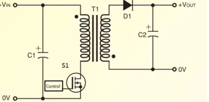
In figure 1 [2] when power switch S1 is ‘on’
with the application of ‘on’ pulse from the
control circuit, the current flows through the
primary winding and energy is stored within
the core. Note that no current can flow
through the secondary because of opposite
dot polarity and hence diode D1 is reversed
bias.
When power switch driving pulse from the
control circuit is removed (during ‘off’ time),
the polarity reverses and the current flows
in the secondary winding.
Available Online At www.ijpret.com The current flows in either the primary or
secondary winding but never in both the
windings at the same time. Thus the so
called fly back transformer is not a
transformer but a coupled inductor.
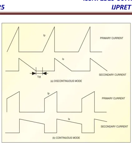
Discontinuous and continuous modes of
operation
A fly back converter, just like any other
topology has two different modes of
operation, discontinuous mode and
continuous mode [2]. A circuit that has been
designed for discontinuous mode will move
into continuous mode when the output
current is increased beyond a certain value.
The waveforms of primary and secondary
currents through the transformer are shown
in figure 2. In the discontinuous mode all the
energy stored in the primary during the
power switch ‘on’ time is completely
delivered to the secondary and to the load
before the next cycle, and there is also a
dead time between the instant the
secondary current reaches zero and the
start of the next cycle.
Figure 2: Primary and secondary currents in
(a) discontinuous and (b) continuous mode
In the continuous mode there is still some
energy left in the secondary at the
beginning of the next cycle. The flyback can
operate in both modes, but it has different
characteristics. The discontinuous mode has
higher peak currents, and therefore it has
higher output voltage spikes during the
turn-off. On the other hand, it has faster
load transient response, lower primary
inductance, and therefore the transformer
can be smaller in size. The reverse recovery
time of the diode is not critical because the
forward current is zero before the reverse
voltage is applied. Conducted EMI noise is
reduced in discontinuous mode because
Available Online At www.ijpret.com current. The continuous mode has lower
peak currents and, therefore, lower output
voltage spikes. Therefore DCM is usually
recommended for high voltage and low
current output applications. Meanwhile,
CCM is preferred for low voltage and
high current output applications.
A change in load resistance means changes
in output currents. Hence, the duty cycle (D)
has to be changed to maintain the desired
output power.
III. DESIGN PROCEDURE
The design procedure will be explained
briefly for a three output isolated flyback
dc-dc converter with specifications given in
Table I:
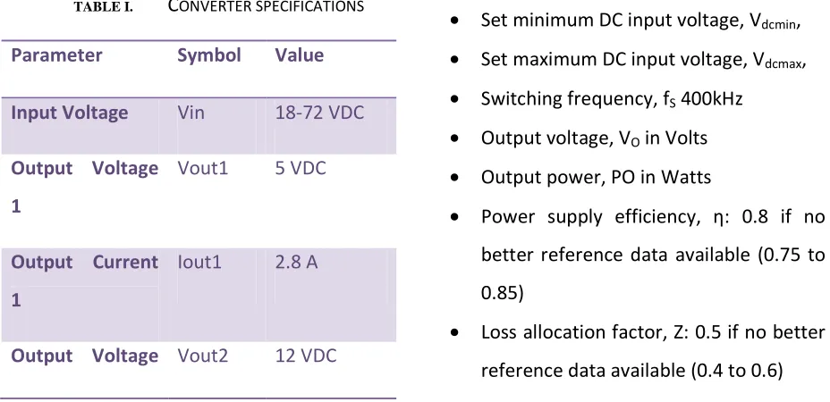
TABLE I. CONVERTER SPECIFICATIONS
Parameter Symbol Value
Input Voltage Vin 18-72 VDC
Output Voltage
1
Vout1 5 VDC
Output Current
1
Iout1 2.8 A
Output Voltage Vout2 12 VDC
2
Output Current
2
Iout2 100 mA
Output Voltage
3
Vout3 -12 VDC
Output Current
3
Iout3 100 mA
Output Power PO 16.7 W
Switching
Frequency
fs 400 kHz
The design of the converter is conducted
using various steps.
Step 1.Determine system requirements
• Set minimum DC input voltage, Vdcmin,
• Set maximum DC input voltage, Vdcmax,
• Switching frequency, fS 400kHz
• Output voltage, VO in Volts
• Output power, PO in Watts
• Power supply efficiency, η: 0.8 if no
better reference data available (0.75 to
0.85)
• Loss allocation factor, Z: 0.5 if no better
Available Online At www.ijpret.com fs is the switching frequency of switcher IC.
Step 2. Determine primary waveform
parameters
The average current is calculated using “Eq.
1” [1].
Peak primary current Ip “Eq. 2” [1] is
calculated from average current Iavg, ripple
to peak current ratio Kp, and maximum duty
cycle Dmax.
Where Kp is less than 1.0 for continuous
mode. Kp is equal to 1.0 for Discontinuous
mode, Dmax is 60%. The ripple current Ir
“Eq.3” is calculated from average current
Iavg, peak primary current Ip, and maximum
duty cycle Dmax.
IV. DESIGN OF MAGNETICS
The design of the transformer is critical
for the desirable operation of the
converter.
Step 4. Determine primary inductance LP
The primary inductance of the transformer
is calculated by using the “Eq.4” [1].
where units are μH, watts, amps and Hz.
Choose the proper core
Ferrite is the most widely used core
material for commercial SMPS applications.
Soft ferrites like NiZn and MnZn are
available. There high resistivity prevents
eddy current losses at high frequency. The
type of the core should be chosen with
regard to system requirements including
number of outputs, physical height, cost
and switching frequency [4]. A flyback
transformer designed for DCM operation
requires a smaller inductance value than
one designed for CCM operation, since the
current ripple (Ir) is much higher. In some
applications, lower inductance may result in
Available Online At www.ijpret.com the efficiency and thermal performance
remain acceptable.
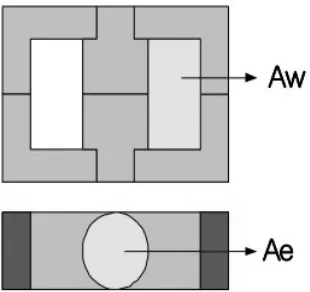
Figure 3: Window area and cross sectional
area
The core type used depends mainly on size
restraints. EFD and EPC cores are used
when a low profile is required [3]. E, EE and
EF are good general cores and can usually
be used with either vertical or horizontal
bobbins. ETD and EER cores are usually
larger, but have a wide winding area, which
makes them particularly good for higher
power designs or multiple output designs.
Once the core type and size are
determined, the following variables are
obtained from the core data sheet. Ae: The
cross sectional area of the core (mm2), Aw:
Winding window area (mm2), Bsat: Core
saturation flux density (tesla). Figure 3
shows the Ae and Aw of a core. The typical
B-H characteristics of ferrite core are
obtained from the datasheets. Since the
saturation flux density (Bsat) decreases as
the temperature increases, the high
temperature characteristics should be
considered. If there is no reference data,
use Bsat = 0.3~0.35T[3]. Minimum no. of
primary winding to avoid core saturation is
found out using “Eq.5” [3].
where Ilimitmax is the maximum current limit
of the switching device.
Reflected output voltage
This parameter is the secondary winding
voltage during diode conduction, reflected
back to the primary through the turn’s ratio
of the transformer. “Eq. 6” [1] is used to
calculate the Vor.
Vds is the average Drain to Source voltage
during Switch ON time which can be
obtained from the datasheet of the
Available Online At www.ijpret.com Np is related to the secondary number of
turns Ns by the ratio between Vor and Vo + Vd
.Thus the no. of secondary can be obtained
by using “Eq. 7” [1].
Step 5. Determine maximum peak inverse
voltages PIVS
The peak inverse voltage across the
secondary rectifier diode is given by “Eq.8”.
Additional or auxiliary output winding
number of turns Nx “Eq. 9” and rectifier
diode peak inverse voltage PIVx “Eq. 8” can
be determined from the desired value for
auxiliary output voltage Vx, auxiliary
rectifier diode forward voltage drop Vdx,
output voltage Vo, output rectifier diode
forward voltage drop Vd, and number of
secondary turns Ns.
V. SIMULATION RESULTS
The three output isolated flyback dc-dc
converter was simulated in LTspice IV circuit
simulator using the elements designed in
the previous section. The equivalent
electrical circuit model for the transformer
is obtained by calculating the inductance of
secondary windings by using the relation
“Eq.10”. Table II gives converter component
values which are used in the simulation.
S
pice equivalent model of the switching IC
was unavailable; hence alternately a pulse
source generating a switching frequency of
400 kHz is used. The voltage controlled
switch along with pulse source is modeled
as PWM. The converter designed using
LTspice IV is shown in figure 4.
TABLE II. CONVERTER COMPONENT VALUES
Component Symbol Values
Primary Winding L1 20μH
Output winding for 5V L3 2.15μH
Output winding for 12V L2 4.26μH
Output winding for 12V L4 10.8μH
Output capacitor for 5V C2 2700μF
Output capacitor for 12V
C1 47μF
Output capacitor for -12V
Available Online At www.ijpret.com Figure 4. Schematic of converter designed
using LTspice IV.
A voltage mode feedback without
compensation network is used. The output
of error amplifier drives the voltage
controlled switch. Thus the gate to source
voltage Vg is shown in figure 5 and the
result of simulation i.e. the output voltages
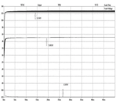
are shown in figure 6.
Figure 5. Gate to source voltage Vg.
Figure 6. Output voltage waveforms.
VI. CONCLUSION
The multiple output isolated flyback dc-dc
converter with three outputs is analyzed in
this paper. The advantage of this topology is
the circuit is simpler and requires less no of
components. The flyback converter can be
operated in CCM or DCM depending on the
load conditions. Hence the duty cycle is
varied to maintain the desired output. The
simulator allows the designer to determine
the correctness and efficiency of a design
before the system is actually constructed.
The calculated values of converter
component differ from the actual values
used in the simulation design. Consider the
output winding for 5V; the actual value of
Available Online At www.ijpret.com 10” gives output voltage less than 5V when
used in simulation. Hence the value of
inductor L3 is changed to 2.15μH in the
simulation design. The reasons for doing
this might be that we are not actually using
the spice model of switcher IC and the
simulation is done just to verify if the design
will work or not. When actual prototype is
generated the results will nearly match with
the calculated values.
REFERENCES
1. AN-16 Flyback Design Methodology.
2. Dinesh Kumar “Design a high-frequency
power transformer based on flyback
topology”.
3. AN4137 Design Guidelines for Off-line
Flyback Converters Using Fairchild Power