Advanced nanomaterials
Cours support
This text is also partially used for the cours
“Introduction to Nanomaterial”
H.Hofmann
Powder Technology Laboratory
IMX
EPFL
Contents
1 INTRODUCTION 6
1.1 WHAT ARE NANOMATERIALS? 6
1.1.1 CLASSIFICATION OF NANOSTRUCTURED MATERIALS 6
1.1.2 WHY SO MUCH INTEREST IN NANOMATERIALS? 8
1.1.3 INFLUENCE ON PROPERTIES BY "NANO-STRUCTURE INDUCED EFFECTS" 9 1.2 SOME PRESENT AND FUTURE APPLICATIONS OF NANOMATERIALS 10 1.3 WHAT ARE THE FUNDAMENTAL ISSUES IN NANOMATERIALS? 13
2 ATOMS, CLUSTERS AND NANOMATERIALS 15
3 NANOCOMPOSITES SYNTHESIS AND PROCESSING 19
3.1 INTRODUCTION 19
3.2 INORGANIC NANOTUBES 20
3.2.1 INTRODUCTION 20
3.2.2 GENERAL SYNTHETIC STRATEGIES 26
3.3 FUNCTIONAL MATERIALS BASED ON SELF-ASSEMBLY OF POLYMERIC SUPRAMOLECULES 28 3.4 MOLECULAR BIOMIMETICS:NANOTECHNOLOGY THROUGH BIOLOGY 32 3.4.1 SELECTION OF INORGANIC-BINDING PROTEINS THROUGH DISPLAY TECHNOLOGIES 34 3.4.2 CHEMICAL SPECIFICITY OF INORGANIC-BINDING POLYPEPTIDES 36
3.4.3 PHYSICAL SPECIFICITY OF PEPTIDE BINDING 37
3.4.4 PEPTIDE-MEDIATED NANOPARTICLE ASSEMBLY 38
3.5 REFERENCES 40
4 MECHANICAL PROPERTIES 41
4.1 INTRODUCTION 41
4.2 METALS 41
4.2.1 GRAIN SIZE EFFECTS IN PLASTICITY AND CREEP 42 4.2.2 METAL PLASTIC DEFORMATION: A COMPARISON BETWEEN CU AND NI NANOPHASE SAMPLES
49
4.3 CERAMICS /NANOCOMPOSITES 56
4.3.1 DENSITY 56
4.3.2 FRACTURE STRENGTH 56
4.3.3 STRENGTHENING AND TOUGHENING MECHANISMS 58
4.3.4 REDUCTION IN PROCESSING FLAW SIZE 60
4.3.5 CRACK HEALING (ANNEALING TREATMENT) 60
4.3.6 TOUGHENING (K-MECHANISMS) 61
4.3.7 GRAIN BOUNDARY STRENGTHENING MECHANISMS 63
4.3.8 THERMAL EXPANSION MISMATCH (SELSING MODEL) 63
4.3.9 AVERAGE INTERNAL STRESSES 64
4.3.10 LOCAL STRESS DISTRIBUTION 67
4.4 FINAL REMARKS ON STRENGTHENING AND TOUGHENING MECHANISMS 67
4.5 REFERENCES 69
5 THERMAL CONDUCTIVITY IN NANOSTRUCTURED MATERIAL 70
5.1 THERMAL CONDUCTIVITY OF THERMAL BARRIER COATINGS 70
5.1.1 THERMAL CONDUCTIVITY 70
5.1.2 LATTICE WAVES 71
5.1.3 INTERACTION PROCESSES 72
5.2 HIGH-TEMPERATURE THERMAL CONDUCTIVITY OF POROUS AL2O3 NANOSTRUCTURES 76
5.2.1 THEORY 76
5.2.2 EXPERIMENT 82
5.2.3 RESULTS AND DISCUSSION 83
5.3 REFERENCES 88
6 THERMODYNAMIC 89
6.1 NANOTHERMODYNAMICS 89
6.1.1 HILL’S THEORY 90
6.1.2 TSALLIS’ GENERALIZATION OF ORDINARY BOLTZMANN-GIBBS THERMOSTATICS 96 6.1.3 THERMODYNAMICS OF METASTABLE PHASE NUCLEATION ON NANOSCALE 100 6.1.4 NANOTHERMODYNAMIC ANALYSES OF CVD DIAMOND NUCLEATION 112 6.2 THERMODYNAMICS OF MELTING AND FREEZING IN SMALL PARTICLES 117
6.3.2 MATHEMATICAL DESCRIPTION FOR NANO-PHASES OF SN-BI ALLOYS 130 6.3.3 PHASE DIAGRAM FOR ISOLATED NANO-PHASES OF SN-BI ALLOYS 133
6.4 CRYSTAL-LATTICE INHOMOGENEOUS STATE 135
6.5 CONCENTRATIONAL INHOMOGENEITY 137
6.6 REFERENCES 140
7 ELECTRONIC AND OPTICAL PROPERTIES OF NANOMATERIALS 141
7.1 INTRODUCTION 141
7.2 METALS 143
7.2.1 INTRODUCTION 143
7.2.2 ELECTRICAL CONDUCTIVITY 154
7.2.3 SURFACE PLASMONS 162
7.3 CARBON NANOTUBES 171
7.3.1 ELECTRONIC STRUCTURE 172
7.3.2 QUANTUM TRANSPORT PROPERTIES 174
7.3.3 NANOTUBE JUNCTIONS AND DEVICES 178
7.4 SEMICONDUCTOR 181
7.4.1 INTRODUCTION 181
7.4.2 BAND GAP MODIFICATION 185
7.4.3 ELECTRICAL PROPERTIES 190
7.4.4 OPTICAL PROPERTIES 212
7.5 REFERENCES 217
8 MAGNETISM 219
8.1 INTRODUCTION 219
8.1.1 CONCEPT 219
8.1.2 PHENOMENA 220
8.2 MAGNETIC PROPERTIES OF SMALL ATOMIC CLUSTERS 222
8.2.1 INTRODUCTION 222
8.2.2 SIZE DEPENDENCE 223
8.2.3 THERMAL BEHAVIOUR 225
8.2.4 RARE EARTH CLUSTERS 226
8.3 SMALL PARTICLE MAGNETISM 226
8.3.1 CLASSIFICATIONS OF MAGNETIC NANOMATERIAL 226
8.3.3 SINGLE DOMAIN PARTICLES 232
8.3.4 SUPERPARAMAGNETISM 239
8.4 MAGNETOELECTRONICS SPINS 252
8.4.1 SPIN-POLARIZED TRANSPORT AND MAGNETORISISTIVE EFFECTS 252
8.4.2 SPIN INJECTION 256
8.4.3 SPIN POLARIZATION 257
8.5 GIANT MAGNETORESISTANCE (GMR) 259
8.6 STORAGE DEVICES 264
8.6.1 MAGNETIC DATA STORAGE : 264
8.6.2 SENSORS: 265
8.7 REFERENCES 266
1 I
NTRODUCTION
1.1 What are nanomaterials?
1.1.1 Classification of Nanostructured Materials
Nanomaterials are materials which are characterised by an ultra fine grain size
(< 50 nm) or by a dimensionality limited to 50 nm. Nanomaterials can be created with
various modulation dimensionalities as defined by Richard W. Siegel: zero (atomic
clusters, filaments and cluster assemblies), one (multilayers), two (ultrafine-grained
overlayers or buried layers), and three (nanophase materials consisting of equiaxed
nanometer sized grains) as shown in the above Figure 1-1.
Figure 1-1 : Definition of nanomaterials following Siegeli
Nanomaterials consisting of nanometer sized crystallites or grains and
interfaces may be classified according to their chemical composition and shape
(dimensionality), as discussed above. According to the shape of the crystallites or
grains we can broadly classify nanomaterials into four categories:
1. clusters or powders (MD=0)
2. Multilayers (MD=1)
3. ultrafine grained overyaers or buried layers (where the layer thickness or
the rod-diameters are <50 nm) (MD=2)
Figure 1-2 : Classification schema for nanomaterials according to their chemical composition and the dimensionality (shape)of the crystallites (structural elements) forming the nanomaterial. The boundary regions of the first and second family of nanomaterials are indicated in black to emphasize the different atomic arrangements in the crystallites and in the boundaries. The chemical composition of the (black) boundary regions and the crystallites is identical in the first family. In the second family, the (black) boundaries are the regions where two crystals of different chemical composition are joined together causing a steep concentration gradient.
The latter three categories can be further grouped into four families as shown in
Figure 1-2.
• In the most simple case (first family in the Figure 1-2), all grains and interfacial regions have the same chemical composition. Eg. Semicrystalline polymers
(consisting of stacked lamellae separated by non-crystalline region),
multilayers of thin film crystallites separated by an amorphous layer
(a-Si:N:H/nc-Si)iietc.
• As the second case, we classify materials with different chemical composition of grains. Possibly quantum well structures are the best example of this family.
• In the third family includes all materials that have a different chemical composition of its forming matter (including different interfaces) eg. Ceramic of
• The fourth family includes all nanomaterials formed by nanometer sized grains (layers, rods or equiaxed crystallites) dispersed in a matrix of different
chemical composition. Precipitation hardened alloys typically belong to this
family. Eg. Nanometer sized Ni3Al precipitates dispersed in a nickel matrix-
generated by annealing a supersaturated Ni-Al solid solution- are an example
of such alloys. Most high-temperature materials used in modern jet engines
are based on precipitation-hardened Ni3Al/Ni alloys.
A large part of this definition has been described in an article by Gleiter.iv,v
1.1.2 Why so much interest in nanomaterials?
These materials have created a high interest in recent years by virtue of their
unusual mechanical, electrical, optical and magnetic properties. Some examples
are given below:
• Nanophase ceramics are of particular interest because they are more ductile at elevated temperatures as compared to the coarse-grained ceramics.
• Nanostructured semiconductors are known to show various non-linear optical properties. Semiconductor Q-particles also show quantum confinement effects
which may lead to special properties, like the luminescence in silicon powders
and silicon germanium quantum dots as infrared optoelectronic devices.
Nanostructured semiconductors are used as window layers in solar cells.
• Nanosized metallic powders have been used for the production of gas tight materials, dense parts and porous coatings. Cold welding properties combined
with the ductility make them suitable for metal-metal bonding especially in the
electronic industry.
• Single nanosized magnetic particles are mono-domains and one expects that also in magnetic nanophase materials the grains correspond with domains,
while boundaries on the contrary to disordered walls. Very small particles have
special atomic structures with discrete electronic states, which give rise to
special properties in addition to the super-paramagnetism behaviour. Magnetic
nano-composites have been used for mechanical force transfer (ferrofluids),
• Nanostructured metal clusters and colloids of mono- or plurimetallic composition have a special impact in catalytic applications. They may serve as
precursors for new type of heterogeneous catalysts (Cortex-catalysts) and
have been shown to offer substantial advantages concerning activity,
selectivity and lifetime in chemical transformations and electrocatalysis (fuel
cells). Enantioselective catalysis were also achieved using chiral modifiers on
the surface of nanoscale metal particles.
• Nanostructured metal-oxide thin films are receiving a growing attention for the realisation of gas sensors (NOx, CO, CO2, CH4 and aromatic hydrocarbons)
with enhanced sensitivity and selectivity. Nanostructured metal-oxide (MnO2)
find application for rechargeable batteries for cars or consumer goods.
Nano-crystalline silicon films for highly transparent contacts in thin film solar cell and
nano-structured titanium oxide porous films for its high transmission and
significant surface area enhancement leading to strong absorption in dye
sensitized solar cells.
• Polymer based composites with a high content of inorganic particles leading to a high dielectric constant are interesting materials for photonic band gap
structure produced by the LIGA.
1.1.3 Influence on properties by "nano-structure induced effects"
For the synthesis of nanosized particles and for the fabrication of
nanostructured materials, laser or plasma driven gas phase reactions,
evaporation-condensation mechanisms, sol-gel-methods or other wet chemical routes like inverse
micelle preparation of inorganic clusters have been used, that will be discussed later.
Most of these methods result in very fine particles which are more or less
agglomerated. The powders are amorphous, crystalline or show a metastable or an
unexpected phase, the reasons for which is far from being clear. Due to the small
sizes any surface coating of the nano-particles strongly influences the properties of
the particles as a whole. Studies have shown that the crystallisation behaviour of
nano-scaled silicon particles is quite different from micron-sized powders or thin films.
• First the size effect, in particular the quantum size effects where the normal bulk electronic structure is replaced by a series of discrete electronic levels,
• and second the surface or interface induced effect, which is important because of the enormously increased specific surface in particle systems.
While the size effect is mainly considered to describe physical properties, the
surface or interface induced effect, plays an eminent role for chemical processing, in
particular in connection with heterogeneous catalysis. Experimental evidence of the
quantum size effect in small particles has been provided by different methods, while
the surface induced effect could be evidenced by measurement of thermodynamic
properties like vapour pressure, specific heat, thermal conductivity and melting point
of small metallic particles. Both types of size effects have also been clearly separated
in the optical properties of metal cluster composites. Very small semiconductor (<10
nm), or metal particles in glass composites, and semiconductor/polymer composites
show interesting quantum effects and non-linear electrical and optical properties.
The numerous examples, which are not complete, by far, indicate that these
materials will most probably gain rapidly increasing importance in the near future. In
general, properties, production and characterisation methods and their inter-relations
are however not yet satisfactorily understood. Hence, efforts need to be made to
enable the directed tailoring of nanophase, nanoscopic and nanocomposite materials
needed for future technical and industrial applications.
1.2 Some present and future applications of nanomaterials
Here we list some of the present and future applications of nanomaterials that
has been reported in recent literature:
Table 1-1 : Some typical properties of nano-structured materials and possibilities of future applications
Bulk
Single magnetic domain
Small mean free path of electrons in a solid Size smaller than wavelength
High & selective optical absorption of metal particles
Formation of ultra fine pores due to superfine agglomeration of particles
Uniform mixture of different kinds of superfine particles
Grain size too small for stable dislocation
Magnetic recording Special conductors
Light or heat absorption, Scattering
Colours, filters, solar absorbers, photovoltaics, photographic material, phototropic material
Molecular Filters
R&D of New Materials
High strength and hardness of metallic materials
Surface/ Interface
Large specific surface area Catalysis, sensors
Large surface area, small heat capacity Heat-exchange materials Combustion Catalysts
Lower sintering temperature
Specific interface area, large boundary area
Superplastic behaviour of ceramics
Cluster coating and metallization
Multi-shell particles
Sintering accelerators
Nano-structured materials
ductile ceramics
Special resistors, temperature sensors
Table 1-2 : Some examples of present and potential applications with significant technological impact:vi
Technology Present Impact Potential Impact
Dispersions and Coatings
Thermal barriers
Optical (visible and UV) barriers
Imaging enhancement
Ink-jet materials
Coated abrasive slurries
Information-recording layers
Enhanced thermal barriers
Multifunctional nanocoatings
Fine particle structure
Super absorbant materials (Ilford paper)
Higher efficiency and lower contamination
Higher density information storage High Surface
Area
Molecular sieves
Drug delivery
Tailored catalysts
Absorption/desorption materials
Molecule-specific sensors
Particle induced delivery
Energy storage (fuel cells, batteries)
Grätzel-type solar cells, Gas sensors
Consolidated Materials
Low-loss soft magnetic materials
High hardness, tough WC/Co cutting tools
Nanocomposite cements
Superplastic forming of ceramics Materials
Ultrahigh-strength, tough structural materials
Magnetic refrigerants
Nanofilled polymer composites Ductile cements
Bio-medical aspects
Functionalised nanoparticles Cell labelling by fluorescent nanoparticles
Local heating by magnetic nanoparticles
Nanodevices GMR read heads Terabit memory and microprocessing Single molecule DNA sizing and sequencing
Biomedical sensors
Nanotubes for high brightness displays
1.3 What are the fundamental issues in nanomaterials?
The fundamental issues in this domain of nanomaterials are:
(1) ability to control the scale (size) of the system,
(2) ability to obtain the required composition -
not just the average composition - but details such as defects, concentration
gradients, etc.,
(3) ability to control the modulation dimensionality,
(4) during the assembly of the nano-sized building blocks, one should be able to
control the extent of the interaction between the building blocks as well as the
architecture of the material itself.
More specifically the following issues have to be considered for the future
development of nanomaterials:
• Development of synthesis and/or fabrication methods for raw materials (powders) as well as for the nanostructured materials.
• Better understanding of the influence of the size of building blocks in nano structured materials as well as the influence of microstructure on the physical,
chemical and mechanical properties of this material.
• Better understanding of the influence of interfaces on the properties of nano-structured material.
• Development of concepts for nanostructured materials and in particular their elaboration.
• Investigation of catalytic applications of mono- and plurimetallic nanomaterials
• Transfer of developed technologies into industrial applications including the development of the industrial scale of synthesis methods of nanomaterials and
nanostructured systems.
improvements in the material properties that are achieved due to the fine
2 A
TOMS
,
CLUSTERS AND NANOMATERIALS
atoms
?
? ?
? ?
? ?
?
? ?
? ?
molecules
cluster
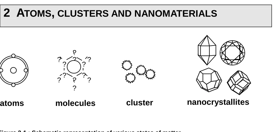
nanocrystallites
Figure 2-1 : Schematic representation of various states of matter
At the beginning of last century, increasing attention was focused on the physical
chemistry of colloidal suspensions. By referring to them as "the world of neglected
dimensions", Oswald was the first to realize that nanoscale particles should display
novel and interesting properties largely dependant on their size and shape.vii
However, it is only in the last two decades that significant interest has been devoted
to inorganic particles consisting of a few hundred or a few dozen atoms, called
clusters. This interest has been extended to a large variety of metals and
semiconductors and is due to the special properties exhibited by these
nanometer-sized particles, which differ greatly from those of the corresponding macrocrystalline
material.
Matter that is constituted of atoms and molecules as such, has been widely classified
and satisfactorily explained. However, an ensemble of atoms, or molecules forming
the so-called ‘Clusters’ are far from being properly understood. Elemental clusters
are held together by various forces depending on the nature of the constituting
atoms:
Inert gas clusters are weakly held together by van-der-waals interactions, eg. (He)n
Semiconductor clusters are held with strong directional covalent bonds, eg. (Si)n
Metallic clusters are fairly strongly held together by delocalised non-directional
No. Of Shells 1 2 3 4 5
No. of atoms M13 M55 M147 M309 M561
Percentage of atoms
92% 76% 63% 52% 45%
Figure 2-2 : Idealized representation of hexagonal close packed full-shell ‘magic number’ clusters.viii Note that as the number of atoms increases, the percentage of surface atoms decreases.
1 10 100 1000 10000 100000
0 10 20 30
Cluster size (nm)
T
o
ta
l
n
o
.
o
f
a
to
m
s
(1)
0 20 40 60 80 100 120
0 5 10 15 20 25
Size of cluster (nm)
Su
rf
a
c
e
a
to
m
s
(
%
)
(2)
Figure 2-3 : (1) Total Number of atoms with size of the cluster. (2) Number of surface atoms for a hypothetical model sphere of diameter 0.5 nm and density 1000 Kgm-3 with a mass of 6.5 10-26 Kg occupying a volume of about 6.5 x 10⁻²⁹ m3 with a geometrical cross-section of 2 x 10-19 m2 (in terms of atomic mass the sphere is considered to have a mass of 40 amu, where 1 amu = 1.67 x 10⁻²⁷ Kg). Calculated by (a) considering dense structures (Square),ix and (b) method suggested by Preining (dark circle).x
Either elemental clusters or a mixture of clusters of different elements constitute the
vast expanding field of materials sciences called ‘nanomaterials’. One has to be clear
right at this stage that clusters are not a fifth state of matter, as sometimes believed,
but they are simply intermediate between atoms on one hand, and solid or liquid
state of matter on the other, with widely varying physical and chemical properties.
Depending on the number of atoms forming the cluster determines the percentage of
atoms that are exposed on the surface of the cluster. An example of such an
increasing size of the cluster as shown in fig: . When an ensemble of atoms add up to
form a few nanometer sized clusters, they form what we call ‘nanoparticles’, since
only a few atoms forming clusters are called ‘molecular clusters’. Agglomeration of a
few atoms have been studied in great details by physicists working with molecular
beams. Today, the mystery related to larger ensemble of atoms (in other words
‘nanomaterial’) are getting clearer due to active research being carried over across
the world over the last decade or two.
Table 2-1 : Idealized representation of the variation of cross section, total mass, number of molecules and the effective surface atoms in clusters. Note (a) considering dense structures (Square),ix and (b) method suggested by Preining (dark circle).x
Size Cross
section
Mass No. Of molecules
Fraction of molecules at surface (%)
(nm) (10-18 m2) (10-25 Kg) a b
0,5 0,2 0,65 1
1 0,8 5,2 8 100 99
2 3,2 42 64 90 80
5 20 650 1000 50 40
10 80 5200 8000 25 20
20 320 42000 64000 12
In the table, we see that the smaller particles contain only a few atoms, practically all
at the surface. As the particle size increases from 1-10 nm, cross-section increases
by a factor of 100 and the mass number of molecules by a factor of 1000. Meanwhile,
the proportion of molecules at the surface falls from 100% to just 25%. For particles
of 20nm size, a little more than 10% of the atoms are on the surface.
Of course this is an idealized hypothetical case. If particles are formed by macro
molecules (that are larger than the present example), number of molecules per
particle will decrease and their surface fraction increase. The electronic properties of
these ensemble of atoms or molecules will be the result of their mutual interactions
so that the overall chemical behaviour of the particles will be entirely different from
the individual atoms or molecules that they are constituted of. They will also be
different from their macroscopic bulk state of the substance in question under the
Size (nm)
Surface area (m2 mol-1)
Surface energy (J mol-1)
1 1.11 x 10⁹ 2.55 x 10⁴
2 5.07 x 10⁸ 1.17 x 10⁴
5 2.21 x 10⁸ 5.09 x 10³
10 1.11 x 10⁸ 2.55 x 10³
20 5.07 x 10⁷ 1.17 x 10³
102 1.11 x 10⁷ 2.55 x 10² 103 (1µm) 1.11 x 10⁶
2.55 x 10
The idea of tailoring properly designed atoms into agglomerates has brought in new
fundamental work in the search for novel materials with uncharacteristic properties.
Among various types of nanomaterials, cluster assembled materials represent an
original class of nanostructured solids with specific structures and properties. In
terms of structure they could be classified in between amorphous and crystalline
materials. In fact, in such materials the short-range order is controlled by the grain
size and no long-range order exists due to the random stacking of nanograins
characteristic of cluster assembled materials. In terms of properties, they are
generally controlled by the intrinsic properties of the nanograins themselves and by
the interactions between adjacent grains. Cluster assembled films are formed by the
deposition of these clusters onto a solid substrate and are generally highly porous
with densities as low as about one half of the corresponding bulk materials densities
and both the characteristic nanostructured morphology and a possible memory effect
of the original free cluster structures are at the origin of their specific properties.xii From recent developments in the cluster source technologies (thermal, laser
3 N
ANOCOMPOSITES
S
YNTHESIS AND
P
ROCESSING
3.1 Introduction
A major goal of material science is to produce hierarchical materials that are
ordered on all length scales, from the molecular (1–100 Å) via the nano (10–100 nm)
to the meso (1–100 mm) scale. In these materials, the larger-scale properties can be
controlled by choosing the appropriate molecular characteristics.
“Nanocomposites” are a special class of materials originating from suitable
combinations of two or more such nanoparticles or nanosized objects in some
suitable technique, resulting in materials having unique physical properties and wide
application potential in diverse areas that can be formed into a useful object which
can be subsequently used. Novel properties of nanocomposites can be derived from
the successful combination of the individual characteristics of parent constituents into
a single material. To exploit the full potential of the technological applications of the
nanomaterials, it is thus extremely important to endow them with good processability.
Nanocomposites are either prepared in a host matrix of inorganic materials (glass,
porous ceramics etc) or by using conventional polymers as one component of the
nanocomposites. The second type of nanocomposites which are a special class of
hybrid materials are termed “polymeric nanocomposites”. These materials are
intimate combinations (up to almost the molecular level) of one or more inorganic
materials (nanoparticles , eg.) with a polymer so that unique properties of the former
can be mixed with the existing qualities of the polymer to result in a totally new
material suitable for novel applications. In most of the cases such combinations
require blending or mixing of the components, taking the polymer in solution or in
3.2 Inorganic Nanotubes
xxi3.2.1 Introduction
In 1991, Iijima observed some unusual structures of carbon under the transmission
electron microscope wherein the graphene sheets had rolled and folded onto
themselves to form hollow structures. Iijima called them nanotubes of carbon which
consisted of several concentric cylinders of grapheme sheets. Graphene sheets are
hexagonal networks of carbon and these layers get stacked one above the other in
the c-direction to form bulk graphite. Following the initial discovery, intense research
has been carried out on carbon nanotubes (CNTs). The nanotubes can be
open-ended or closed by caps containing five-membered rings. They can be multi-
(MWNTs) or singlewalled (SWNTs). We show a typical high-resolution electron
microscope (HREM) image of a multi-walled nanotube in Figure 3-1.
Figure 3-1 : A typical TEM image of a closed, multi-walled carbon nanotube. The separation between the graphite layers is 0.34 nm. [C.N.R. Rao, M. Nath, Inorganic nanotubes, Dalton Trans., 2003, p.p. 1-24]
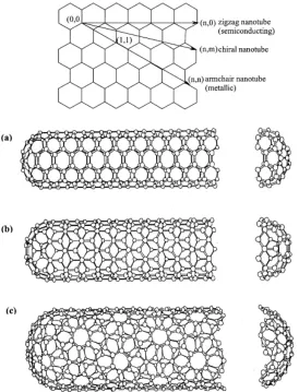
Depending on the way the graphene sheets fold, nanotubes are classified as
armchair, zigzag or chiral as shown in Figure 3-2. The electrical conductivity of the
Figure 3-2 : Schematic representation of the folding of a graphene sheet into (a) zigzag, (b) armchair and (c) chiral nanotubes. [C.N.R. Rao, M. Nath, Inorganic nanotubes, Dalton Trans., 2003, p.p. 1-24]
Several layered inorganic compounds possess structures comparable to the structure
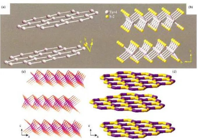
of graphite, the metal dichalcogenides being important examples. The metal
dichalcogenides, MX2 (M = Mo, W, Nb, Hf; X = S, Se) contain a metal layer
sandwiched between two chalcogen layers with the metal in a trigonal pyramidal or
octahedral coordination mode. The MX2 layers are stacked along the c-direction in
ABAB fashion. The MX2 layers are analogous to the single graphene sheets in the
Figure 3-3 : Comparison of the structures of (a) graphite and inorganic layered compounds such as (b) NbS2/TaS2; (c) MoS2; (d) BN. In the layered dichalcogenides, the metal is in trigonal prismatic (TaS2) or octahedral coordination (MoS2). [C.N.R. Rao, M. Nath, Inorganic nanotubes, Dalton Trans., 2003, p.p. 1-24]
When viewed parallel to the c-axis, the layers show the presence of dangling bonds
due to the absence of an X or M atom at the edges. Such unsaturated bonds at the
edges of the layers also occur in graphite. The dichalcogenide layers are unstable
towards bending and have a high propensity to roll into curved structures. Folding in
the layered transition metal chalcogenides (LTMCs) was recognized as early as
1979, well before the discovery of the carbon nanotubes. Rag-like and tubular
structures of MoS2 were reported by Chianelli who studied their usefulness in
catalysis.
The folded sheets appear as crystalline needles in low magnification transmission
electron microscope (TEM) images, and were described as layers that fold onto
Figure 3-4 : Low-magnification TEM images of (a) highly folded MoS2 needles and (b) a rolled sheet of MoS2 folded back on itself. [C.N.R. Rao, M. Nath, Inorganic nanotubes, Dalton Trans., 2003, p.p. 1-24]
These structures indeed represent those of nanotubes. Tenne et al xxii first demonstrated that Mo and W dichalcogenides are capable of forming nanotubes
(Figure 3-5 a).
Figure 3-5 : TEM images of (a) a multi-walled nanotube of WS2 and (b) hollow particles (inorganic fullerenes) of WS2. [C.N.R. Rao, M. Nath, Inorganic nanotubes, Dalton Trans., 2003, p.p. 1-24]
Closed fullerene-type structures (inorganic fullerenes) also formed along with the
nanotubes (Figure 3-5 b). The dichalcogenide structures contain concentrically
nested fullerene cylinders, with a less regular structure than in the carbon nanotubes.
Accordingly, MX2 nanotubes have varying wall thickness and contain some
amorphous material on the exterior of the tubes. Nearly defect-free MX2 nanotubes
are rigid as a consequence of their structure and do not permit plastic deformation.
Figure 3-6 : Schematic illustration of the bending of a MoS2 layer. [C.N.R. Rao, M. Nath, Inorganic nanotubes, Dalton Trans., 2003, p.p. 1-24]
Considerable progress has been made in the synthesis of the nanotubes of Mo and
W dichalcogenides in the last few years (Table 3-1 and Table 3-2).
Table 3-1 : Synthetic strategies for various chalcogenide nanotubes [C.N.R. Rao, M. Nath, Inorganic nanotubes, Dalton Trans., 2003, p.p. 1-24]
There has been some speculation on the cause of folding and curvature in the
LTMCs. Stoichiometric LTMC chains and layers such as those of TiS2 possess an
inherent ability to bend and fold, as observed in intercalation reactions.
The existence of alternate coordination and therefore of stoichiometry in the LTMCs
may also cause folding. Lastly, a change in the stoichiometry within the material
would give rise to closed rings.
Transition metal chalcogenides possess a wide range of interesting physical
properties. They are widely used in catalysis and as lubricants. They have both
semiconducting and superconducting properties (see paragraph 7). With the
synthesis and characterization of the fullerenes and nanotubes of MoS2 and WS2, a wide field of research has opened up enabling the successful synthesis of nanotubes
of other metal chalcogenides. It may be recalled that the dichalcogenides of many of
the Group 4 and 5 metals have layered structures suitable for forming nanotubes.
Curved structures are not only limited to carbon and the dichalcogenides of Mo and
W. Perhaps the most well-known example of a tube-like structure with diameters in
the nm range is formed by the asbestos mineral (chrysotil) whose fibrous
characteristics are determined by the tubular structure of the fused tetrahedral and
inorganic porous solids is varied by a suitable choice of the template. However, in
contrast to the synthesis of porous compounds, the synthesis of nanotubes is
somewhat more difficult.
Nanotubes of oxides of several transition metals as well as of other metals have been
synthesized employing different methodologies. Silica nanotubes were first produced
as a spin-off product during the synthesis of spherical silica particles by the
hydrolysis of tetraethylorthosilicate (TEOS) in a mixture of water, ammonia, ethanol
and D,L-tartaric acid. Since selfassembly reactions are not straightforward with
respect to the desired product, particularly its morphology, templated reactions have
been employed using carbon nanotubes to obtain nanotube structures of metal
oxides. Oxides such as V2O5 have good catalytic activity in the bulk phase. Redox
catalytic activity is also retained in the nanotubular structure. There have been efforts
to prepare V2O5 nanotubes by chemical methods as well.
Boron nitride (BN) crystallizes in a graphite-like structure and can be simply viewed
as replacing a C–C pair in the graphene sheet with the iso-electronic B–N pair. It can,
therefore, be considered as an ideal precursor for the formation of BN nanotubes.
Replacement of the C–C pairs partly or entirely by the B–N pairs in the hexagonal
network of graphite leads to the formation of a wide array of two-dimensional phases
that can form hollow cage structures and nanotubes. The possibility of replacing C–C
pairs by B–N pairs in the hollow cage structure of C60 was predicted and verified
experimentally. BN-doped carbon nanotubes have been prepared. Pure BN
nanotubes have been generated by employing several procedures, yielding
nanotubes with varying wall thickness and morphology. It is therefore quite possible
that nanotube structures of other layered materials can be prepared as well. For
example, many metal halides (e.g., NiCl2), oxides (GeO2) and nitrides (GaN)
crystallize in layered structures. There is considerable interest at present to prepare
exotic nanotubes and to study their properties.
3.2.2 General synthetic strategies
Several strategies have been employed for the synthesis of carbon nanotubes. They
are generally made by the arc evaporation of graphite or by the pyrolysis of
hydrocarbons such as acetylene or benzene over metal nanoparticles in a reducing
method of making carbon nanotubes. In addition to the above methods, carbon
nanotubes have been prepared by laser ablation of graphite or electron-beam
evaporation. Electrochemical synthesis of nanotubes as well as growth inside the
pores of alumina membranes have also been reported. The above methods broadly
fall under two categories. Methods such as the arc evaporation of graphite employ
processes which are far from equilibrium. The chemical routes are generally closer to
equilibrium conditions. Nanotubes of metal chalcogenides and boron nitride are also
prepared by employing techniques similar to those of carbon nanotubes, although
there is an inherent difference in that the nanotubes of inorganic materials such as
MoS2 or BN would require reactions involving the component elements or
compounds containing the elements. Decomposition of precursor compounds
containing the elements is another possible route.
Nanotubes of dichalcogenides such as MoS2, MoSe2 and WS2 are also obtained by
employing processes far from equilibrium such as arc discharge and laser ablation.
By far the most successful routes employ appropriate chemical reactions. Thus,
MoS2 and WS2 nanotubes are conveniently prepared starting with the stable oxides,
MoO3 and WO3. The oxides are first heated at high temperatures in a reducing atmosphere and then reacted with H2S. Reaction with H2Se is used to obtain the
selenides. Recognizing that the trisulfides MoS3 and WS3 are likely to be the
intermediates in the formation of the disulfide nanotubes, the trisulfides have been
directly decomposed to obtain the disulfide nanotubes. Diselenide nanotubes have
been obtained from the metal triselenides. The trisulfide route is indeed found to
provide a general route for the synthesis of the nanotubes of many metal disulfides
such as NbS2 and HfS2. In the case of Mo and W dichalcogenides, it is possible to
use the decomposition of the precursor ammonium salt, such as (NH4)2MX4 (X = S,
Se; M = Mo, W) as a means of preparing the nanotubes. Other methods employed
for the synthesis of dichalcogenide nanotubes include hydrothermal methods where
the organic amine is taken as one of the components in the reaction mixture (Table
3-1 and Table 3-2).
The hydrothermal route has been used for synthesizing nanotubes and related
structures of a variety of other inorganic materials as well. Thus, nanotubes of
Surfactant-assisted synthesis of CdSe and CdS nanotubes has been reported. Here
the metal oxide reacts with the sulfidizing/selenidizing agent in the presence of a
surfactant such as TritonX.
Sol–gel chemistry is widely used in the synthesis of metal oxide nanotubes, a good
example being that of silica and TiO2. Oxide gels in the presence of surfactants or
suitable templates form nanotubes. For example, by coating carbon nanotubes
(CNTs) with oxide gels and then burning off the carbon, one obtains nanotubes and
nanowires of a variety of metal oxides including ZrO2, SiO2 and MoO3. Sol–gel
synthesis of oxide nanotubes is also possible in the pores of alumina membranes. It
should be noted that MoS2 nanotubes are also prepared by the decomposition of a
precursor in the pores of an alumina membrane.
Boron nitride nanotubes have been obtained by striking an electric arc between HfB2
electrodes in a N2 atmosphere. BCN and BC nanotubes are obtained by arcing
between B/C electrodes in an appropriate atmosphere. A greater effort has gone into
the synthesis of BN nanotubes starting with different precursor molecules containing
B and N. Decomposition of borazine in the presence of transition metal nanoparticles
and the decomposition of the 1 : 2 melamine–boric acid addition compound yield BN
nanotubes. Reaction of boric acid or B2O3 with N2 or NH3 at high temperature in the
presence of activated carbon, carbon nanotubes or catalytic metal particles has been
employed to synthesize BN nanotubes.
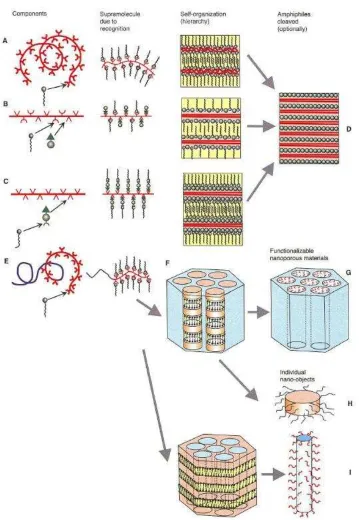
3.3 Functional Materials Based on Self-Assembly of
Polymeric Supramolecules
xxivHere, we describe some possibilities for preparing functional polymeric materials
using the "bottom-up" route, based on self-assembly of polymeric supramolecules.
Directed assembly leads to the control of structure at several length scales and
anisotropic properties. The physical bonds within the supramolecules allow controlled
cleavage of selected constituents. The techniques constitute a general platform for
constructing materials that combine several properties that can be tuned separately.
To achieve enhanced functionalities, the principal periodicity is at ~10 to 2000 Å.
There are established ways to accomplish this by using various architectures of block
copolymers, in which the structure formation is based on self-organization, that is, on
architecture, block length, and temperature, it is possible to obtain lamellar,
cylindrical, spherical, gyroid, or more complicated structures in the 100 to 2000 Å
range. Also, rodlike moieties within the block copolymers can be used to further tailor
the structures in terms of shape persistency. However, self-organization renders only
the local structures. To fully realize the opportunities offered by the symmetry of the
self-organized structures to prepare materials with a strongly directional variation of
properties, additional mechanisms and interactions have to be invoked to obtain
macroscale order. This may be achieved by flow, by electric or magnetic fields, or by
using topographically patterned surfaces. One can further extend the structural
complexity by mixing block copolymers with additional polymers and inorganic
additives, thereby increasing the self-organization periods into the photonic band gap
regime. Block copolymers have also been used as templates for the synthesis of
inorganic materials, even allowing the creation of separate ceramic nano-objects.
To achieve even greater structural complexity and functionality, we can combine
recognition with self-organization. Lehn elaborated on the concept of recognition in
synthetic materials, whereby two molecules with molecularly matching
complementary interactions and shapes recognize each other and form a
receptor-substrate supramolecule. To achieve sufficient bonding, synergism of several
physical interactions is often required. Homopolymerlike supramolecules have been
constructed based on a combination of four hydrogen bonds and through
coordination. Supramolecules can spontaneously assemble or self-organize to form
larger structures.
A general framework for forming complex functional materials emerges. Molecules
are constructed that recognize each other in a designed way. The subsequent
supramolecules in turn form assemblies or self-organize, possibly even forming
hierarchies. The overall alignment of the local structures can be additionally improved
by electric or magnetic fields, by flow, or by patterned surfaces.
To illustrate recognition-driven supramolecule formation in polymers and the
subsequent self-organization and preparation of functional materials and
nano-objects, we focus on the comb-shaped architecture (Figure 3-7) encouraged by the
result from cleaving the side chains from a cylinder-within-lamellae structure. Without loss of generality, (A) is shown as a flexible polymer, whereas (B) and (C) are shown as rodlike chains. [O. Ikkala, G.T. Brinke, Functional Materials Based on Self-assembly of polymeric supramolecules, Science, New Series, Vol. 295, No. 5564 (Mar. 29, 2002), pp. 2407-2409]
The simplest case is a flexible polymer having bonding sites along its backbone
(Figure 3-7 A). Therefore, the backbone is typically polar, and repulsive nonpolar side
groups can be connected by complementary bonds, leading to comb-shaped
supramolecules, which in turn self-organize. We have extensively used hydrogen
bonding or coordination to bond side chains to the polymer backbone. Antonietti et
al.xxv have used ionic interactions in polyelectrolyte-surfactant complexes to form comb-shaped polyelectrolyte surfactant complexes. The resulting self-organized
multidomain structures may be aligned, using, for example, flow, in order to approach
monodomains. One can also tune the properties by tailoring the nature of the side
chains. For example, if the side chains are partly fluorinated, low surface energy
results, which allows for applications that lead to reduced friction. In another case,
the backbone consists of the double helix of DNA, and self-organization is achieved
by ionically bonding cationic liposomes or cationic surfactants to the anionic
phosphate sites. This allows for materials design beyond the traditional scope of
biochemical applications. For example, dyes can be intercalated into the helices,
suppressing their aggregation tendency and leading to promising properties as
templates for photonic applications. In such a structure, the polymer backbone may
contain two or even more kinds of binding sites where different additives can be
bonded (Figure 3-7 B). Side chains can also have two separate functions. For
example, in addition to providing a repulsive side chain required for self-organization,
the side chains may contain an acidic group that acts as a dopant for a conjugated
polymer such as polyaniline, which leads to electronic conductivity. To introduce
further degrees of freedom in tailoring the self-organized phases and their
processing, polyaniline may first be doped by a substance such as camphor
sulphonic acid and subsequently connected to hexyl resorcinol molecules using their
two hydrogen bonds (Figure 3-7 C). The alkyl chains of the hydrogen-bonded hexyl
resorcinol molecules act as plasticizers, leading to thermoplastic processibility of the
otherwise infusible polymer. They enforce self-organization where camphor sulfonic
polymers, such as polypyridine, which consists of para-coupled heteroaromatic rings.
Its optical properties can be tuned based on camphor sulphonic acid. Subsequent
hydrogen bonding with alkyl resorcinol creates comb-shaped supramolecules, which
self-organize in lamellae in such a way that the material is fluid even without
additional solvents. Such a fluid state incorporating rigid polymeric rods is uncommon
and allows processing toward monodomains where the rods are aligned. Ultimately,
the plasticizing hydrogen-bonded alkyl resorcinol molecules can be removed by
evaporation in a vacuum oven, thus interlocking the chains in solid stable films
(Figure 3-7 D). In this way, efficient polarized luminance has been achieved.
To increase complexity, one can incorporate structural hierarchies. This can be
accomplished by applying within a single material different self-organization and
recognition mechanisms operating at different length scales. For example, block
copolymeric self-organization at the 100 to 2000 Å length scale and
polymer-amphiphile self-organization at the 10 to 60 Å length scale can be combined (Figure
3-7 E). After selective doping of one block, conductivity can be switched based on a
sequence of phase transitions.
3.4 Molecular biomimetics: Nanotechnology through
biology
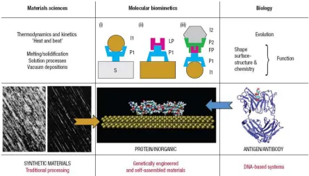
xxviMolecular biomimetics. This is the marriage of materials science engineering and
molecular biology for development of functional hybrid systems, composed of
inorganics and inorganic-binding proteins. The new approach takes advantage of
DNA-based design, recognition,and self-assembly characteristics of biomolecules.
Traditional materials science engineering produces materials (for example,
medium-carbon steels depicted in the bright- and dark-field TEM images), that have been
successfully used over the last century. Molecular biology focuses on structure–
Figure 3-8 : In molecular biomimetics, inorganic-binding proteins could potentially be used as (i) linkers for nanoparticle immobilization; (ii) functional molecules assembled on specific substrates; and (iii) heterobifunctional linkers involving two (or more) binding proteins linking several nanoinorganic units. (I1: inorganic-1,I2: Inorganic-2, P1 and P2: inorganic specific proteins, LP:linker protein, FP: fusion protein). [Sarikaya, C. Tamerler, A.K.Y. Jen, K. Schulten F. Baneyx, Molecular biomimetics: nanotechnology through biology, Nature Materials, vol 2, 2003, p.p. 577-585]
In molecular biomimetics, a marriage of the physical and biological fields, hybrid
materials could potentially be assembled from the molecular level using the
recognition properties of proteins (Figure 3-8) under the premise that inorganic
surface-specific polypeptides could be used as binding agents to control the
organization and specific functions of materials.Molecular biomimetics simultaneously
offers three solutions to the development of heterofunctional nanostructures.
• The first is that protein templates are designed at the molecular level through genetics. This ensures complete control over the molecular structure of the
protein template (that is, DNA-based technology).
• The second is that surface-specific proteins can be used as linkers to bind synthetic entities, including nanoparticles, functional polymers, or other
nanostructures onto molecular templates (molecular and nanoscale
recognition).
co-process for achieving complex nano-, and possibly hierarchical structures,
similar to those found in nature (self-assembly).
The current knowledge of protein-folding predictions and surface-binding chemistries
does not provide sufficiently detailed information to perform rational design of
proteins. To circumvent this problem, massive libraries of randomly generated
peptides can be screened for binding activity to inorganic surfaces using phage and
cell-surface display techniques. It may ultimately be possible to construct a
‘molecular erector’ set, in which different types of proteins, each designed to bind to a
specific inorganic surface, could assemble into intricate, hybrid structures composed
of inorganics and proteins. This would be a significant leap towards realizing
molecularly designed, genetically engineered technological materials.
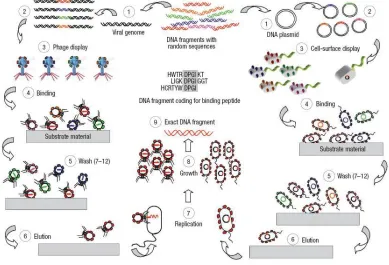
3.4.1 Selection of inorganic-binding proteins through display
technologies
There are several possible ways of obtaining polypeptide sequences with specific
affinity to inorganics. A number of proteins may fortuitously bind to inorganics,
although they are rarely tested for this purpose. Inorganic-binding peptides may be
designed using a theoretical molecular approach similar to that used for
pharmaceutical drugs. This is currently impractical because it is time consuming and
expensive. Another possibility would be to extract biomineralizing proteins from hard
tissues followed by their isolation, purification and cloning. Several such proteins
have been used as nucleators, growth modifiers, or enzymes in the synthesis of
certain inorganics. One of the major limitations of this approach is that a given hard
tissue usually contains many proteins, not just one, all differently active in
biomineralization and each distributed spatially and temporally in complex ways.
Furthermore, tissue-extracted proteins may only be used for the regeneration of the
inorganics that they are originally associated with, and would be of limited practical
use. The preferred route, therefore, is to use combinatorial biology techniques. Here,
a large random library of peptides with the same number of amino acids, but of
different sequences, is used to mine specific sequences that strongly bind to a
chosen inorganic surface.
Since their inception, well-established in vivo combinatorial biology protocols (for
identify biological ligands and to map the epitope (molecular recognition site) of
antibodies. Libraries have also been screened for various biological activities, such
as catalytic properties or altered affinity and specificity to target molecules in many
applications including the design of new drugs, enzymes, antibodies, DNA-binding
proteins and diagnostic agents. The power of display technologies relies on the fact
that an a priori knowledge of the desired amino acid sequence is not necessary, as it
can simply be selected and enriched if a large enough population of random
sequences is available. In vitro methods, such as ribosomal and messenger RNA
display technologies, have been developed for increased library size (1015) compared to those of in vivo systems (107–10).
Combinatorial biology protocols can be followed in molecular biomimetics to select
polypeptide sequences that preferentially bind to the surfaces of inorganic
compounds chosen for their unique physical properties in nano- and biotechnology.
Libraries are generated by inserting randomized oligonucleotides within certain
genes encoded on phage genomes or on bacterial plasmids (step 1 in Figure 3-9).
This leads to the incorporation of a random polypeptide sequence within a protein
residing on the surface of the organism (for example, the coat protein of a phage or
an outer membrane or flagellar protein of a cell; step 2). The eventual result is that
each phage or cell produces and displays a different, but random peptide (step 3). At
this stage, a heterogeneous mixture of recombinant cells or phages are contacted
with the inorganic substrate (step 4).Several washing cycles of the phages or the
cells eliminate non-binders by disrupting weak interactions with the substrate (step
5). Bound phages or cells are next eluted from the surfaces (step 6). In PD, the
eluted phages are amplified by reinfecting the host (step 7). Similarly in CSD, cells
are allowed to grow (steps 7, 8). This step completes a round of biopanning.
Generally, three to five cycles of biopanning are repeated to enrich for tight binders.
Finally, individual clones are sequenced (step 9) to obtain the amino acid sequence
of the polypeptides binding to the target substrate material.
3.4.2 Chemical specificity of inorganic-binding polypeptides
A genetically engineered polypeptide for inorganics (GEPI) defines a sequence of
amino acids that specifically and selectively binds to an inorganic surface. The
surface could be well defined, such as a single crystal or a nanostructure. It might
also be rough, or totally non-descriptive, such as a powder. Researchers have
focused on using materials that can be synthesized in aqueous environments under
physiological conditions (biocompatible) and that exhibit fairly stable surface
structures and compositions. These include noble metals (Pt and Pd) as well as
oxide semiconductors (Cu2O and ZnO) that were biopanned using either PD or
flagellar display (both studies unpublished). Some of the identified binders as well as
sequences selected by other researchers are listed in Table 3-3.
3.4.3 Physical specificity of peptide binding
Ideally, selection of sequences should be performed using an inorganic material of
specific morphology, size, crystallography or surface stereochemistry. In practice,
surfaces with various morphological features. On the other hand, because powders
are non-descriptive, the selected polypeptides may exhibit little or no homology and
‘solve’ the binding problem through different strategies. Binders selected for a given
size, morphology, crystallography or stereochemistry may share a higher degree of
homology. For example, a GEPI binding to a material of a certain size may also bind
to a smaller particle of the same material, but less strongly. Similarly, a GEPI binding
strongly to a specific crystallographic surface may bind with an altered affinity to
another surface of the same material. Finally, a GEPI strongly binding to a material of
composition A may bind less strongly to a material B with a different composition but
having similar structure (for example, perovskites). Therefore, if one seeks highly
specific binders, the physical and chemical characteristics of the material must be
known. An alternative approach is that, once a relatively large number of binders
have been identified by panning on powders, a subset specific for morphology, size
or surface could be identified on well-defined materials.
3.4.4 Peptide-mediated nanoparticle assembly
Organization and immobilization of inorganic nanoparticles in two- or
three-dimensional geometries are fundamental in the use of nanoscale effects.
a) b) c)
d) e)
Figure 3-10 : Effect of GEPI on nanocrystal morphology. a–c, One of the two mutants (RP1) from a library of goldbinding GEPIs were tested in the formation of flat gold particles, shown in a, similar to those formed under acidic (b) or boiling (c) conditions. Particles formed in the presence of vector-encoded alkaline phosphatase and neutral conditions do not result in morphological change of gold particles (not shown). d-e, The atomic force microscope images show quantum (GaInAs) dots assembled on GaAs substrate; d, through high-vacuum (molecular beam epitaxy) strain-induced self-assembly, and e, through 7-repeat GBP1. f, Schematic illustration of e. PS: polystyrene substrate, GA: glutaraldehyde, GBP: 7- repeat GBP1, and gold: 12-nm-diameter colloidal gold particles. [Sarikaya, C. Tamerler, A.K.Y. Jen, K. Schulten F. Baneyx, Molecular biomimetics: nanotechnology through biology, Nature Materials, vol 2, 2003, p.p. 577-585]
For example, quantum dots can be produced using vacuum techniques, such as
molecular beam epitaxy, shown in Figure 3-10 d for the GaInAs/GaAs system.
However, this can only be accomplished under stringent conditions of high
temperature, very low pressures and a toxic environment. A desirable alternative
would be not only to synthesize inorganic nanodots under mild conditions, but also to
immobilize/self-assemble them. Inorganic particles have been functionalized with
synthetic molecules, including thiols and citrates, and with biological molecules, such
as lipids, amino acids, polypeptides and ligand-functionalized DNA. Using the
recognition properties of the coupling agents, novel materials have been generated
and controlled growth has been achieved. These molecules, however, do not exhibit
specificity for a given material. For example, thiols couple gold as well as silver
nanoparticles in similar ways. Likewise, citrate ions cap noble metals indiscriminately.
A desirable next step would be to use GEPIs that specifically recognize inorganics for
nanoparticle assembly. An advantage of this approach is that GEPI can be
genetically or synthetically fused to other functional biomolecular units or ligands to
produce heterobifunctional (or multifunctional) molecular entities. Figure 3-10 e and f
shows the assembly of nanogold particles on GBP1-coated flat polystyrene surfaces,
which resembles the distribution of quantum dots obtained by high-vacuum
deposition techniques (Figure 3-10 d). The homogenous decoration of the surface
with nanogold suggests that proteins may be useful in the production of tailored
nanostructures under ambient conditions and aqueous solutions. Furthermore, the
arrays to produce inorganic particles through templating using, for example, dip-pen
lithography.
3.5 References
Sarikaya, C. Tamerler, A.K.Y. Jen, K. Schulten F. Baneyx, Molecular biomimetics:
nanotechnology through biology, Nature Materials, vol 2, 2003, p.p. 577-585
O. Ikkala, G.T. Brinke, Functional Materials Based on Self-assembly of polymeric
supramolecules, Science, New Series, Vol. 295, No. 5564 (Mar. 29, 2002), pp.
2407-2409
4
M
ECHANICAL PROPERTIES
4.1 Introduction
One of the very basic results of the physics and chemistry of solids is the insight that
most properties of solids depend on the microstructure, i.e. the chemical composition,
the arrangement of the atoms (the atomic structure) and the size of a solid in one,
two or three dimensions. In other words, if one changes one or several of these
parameters, the properties of a solid vary. The most well-known example of the
correlation between the atomic structure and the properties of a bulk material is
probably the spectacular variation in the hardness of carbon when it transforms from
diamond to graphite. The important aspects related to structure are:
• atomic defects, dislocations and strains
• grain boundaries and interfaces
• porosity
• connectivity and percolation
• short range order
Defects are usually absent in either metallic or ceramic clusters of
nanoparticles because dislocations are basically unstable or mobile. The stress field
around a dislocation (or the electrostatic potential around charges and currents)
have to satisfy the Laplace equation: ∇2Φ = 0. This sets up an image dislocation which pulls the defect out of the particle.
When these clusters are assembled under uniaxial pressure into a pellet, for
example, it is found that the individual clusters are packed very tightly into a
polycrystalline solid. Cluster-assembled materials often show close to 100% density.
A fully consolidated nanophase material looks very much like a normal, dense
polycrystalline aggregate, but at a far smaller scale.
4.2 Metals
(described by relevant “size” parameters). The full characterization of these
parameters is the domain of quantitative metallurgy.
Most of these size effects come about because of the microstructural constraint to
which a particular physical mechanism is subjected. Consider the classic case of
strengthening a metallic matrix by particles or grain boundaries: lattice dislocations
are forced, by the microstructural constraint, to bow out or pile up, which requires an
external stress characteristic of a microstructural parameter. The wall thickness
relative to the size of the microstructural inhomogeneity can control the macroscopic
behaviour.
In general, it is therefore the competition or coupling between two different size
dependencies that determines the properties of a material. One thus has to deal with
the interaction of two length scales: (1) is the dimension characteristic of the physical
phenomenon involved, called the characteristic length. (2) is some microstructural
dimension, denoted as the size parameter.
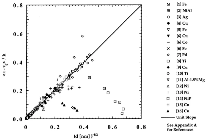
4.2.1 Grain size effects in plasticity and creep
4.2.1.1 Hall-Petch effects.
Strengthening of polycrystalline materials by grain size refinement is
technologically attractive because it generally does not adversely affect ductility
and toughness. The classical effect of grain size on yield stress (
τ
) can, among other possibilities, be explained by a model invoking a pile-up of dislocationsagainst grain boundaries, which results in a dependence of the hardening
increment kHP on the square root of the grain size D
D kHP
=
τ (4. 1)
Where kHP is a constant. This is the classical Hall-Petch effect.
In Figure 4-1, some of the available data have been plotted in a
Figure 4-1 : Compilation of yield stress data for several metallic systems. [R.A. Masumura, P.M. Hazzledine, C.S. Pande, Yield stress of fine grained materials, 1998, Acta-Materialia]
It is seen that the yield stress-grain size exponent for relatively large grains
appears to be very close to -0.5 and generally this trend continues until the very fine
grain regime (~100 nm) is reached. The reported data show three different regions:
1. A region from single crystal to a grain size of about 1 mm where the classical
Hall-Petch description can be used.
2. A region for grain sizes ranging from about 1 mm to about 30 nm where the
Hall-Petch relation roughly holds, but deviates from the classical -0.5
exponent to a value near zero (to ascertain such behaviour, a wide range of
grain sizes extending into the ultra-fine grain size regime is required).
3. A region beyond a very small critical grain size where the Hall-Petch slope is
essentially zero, with no increase in strength on decreasing grain size or
where the strength actually decreases with decreasing grain size.
There is universal agreement regarding the first region, i.e. relatively large grain
sizes. Early hardness measurements had already established a distinct increase in
hardness as grain sizes decrease as compared to their annealed coarse grained
counterparts, and this increase follows the Hall-Petch relationship reasonably well.
deformation mode and lower shear modulus. Indeed, the lower modulus has been
ascribed to a decrease in bulk density. Additional complications arise due to
impurities at the grain boundaries such as oxides and impurities inside the grain
such as trapped or diffused gas. In spite of the above difficulties, once the totality of
the data is taken into consideration, it is fairly safe to conclude that the increase in
strength on grain refinement in the middle region is somewhat less than predicted by
the Hall-Petch relation.
The third region is much more controversial and is going to be discussed later.
4.2.1.2 Limits to Hall-Petch behaviour: dislocation curvature vs. grain size.
Whereas many metallic materials obey such a relationship over several
orders of magnitude in grain size, it is inevitable that the reasoning behind equation
D kHP
=
τ (4. 1) must break down for very small grains. A clear limit for the
occurrence of dislocation plasticity in a poly-crystal is given by the condition th

![Figure 4-2 : Grain size strengthening, as explained by pile-ups of dislocation loops against grain constraints: A comparative review, 1998, Acta Meteriala]fits into a grain of size boundaries (a)](https://thumb-us.123doks.com/thumbv2/123dok_us/608934.2060667/44.595.194.420.424.640/figure-strengthening-explained-dislocation-constraints-comparative-meteriala-boundaries.webp)