Please cite this article as: D. Nath, S. N. Pradhan, Low DropoutBased Noise Minimization of Active Mode Power Gated Circuit, International Journal of Engineering (IJE), IJE TRANSACTIONS C: Aspects Vol. 31, No. 9, (September 2018) 1546-1552
International Journal of Engineering
J o u r n a l H o m e p a g e : w w w . i j e . i rLow Dropout
Based Noise Minimization of Active Mode Power Gated Circuit
D. Nath*, S. N. Pradhan
Department of Electronics & Communication Engineering, National Institute of Technology Agartala, Agartala, India
P A P E R I N F O
Paper history: Received 14 August 2016
Received in revised form 02 December 2017 Accepted 04 February 2018
Keywords: Architecture Power-gating Data-retention Leakage Noise
Low-dropout Voltage
A B S T R A C T
The presence of package inductance induces large voltage fluctuation (bounce noise) on the power rail during power down to power up transition in the power gating circuit that may cause unwanted transitions in neighboring circuits. In this work, a power gating architecture is developed for minimizing power in active mode. Noise for the architecture has also been analyzed. The effect of various noise minimization approaches for reducing power supply noise have been evaluated in power gating architecture. A new concept of noise minimization technique using Low Dropout Voltage Regulator has been proposed in this paper. The amount of charge in the internal nodes that passes through the sleep transistor during the wake-up transition has been controlled by the proposed noise minimization techniques. The Low Dropout Voltage Regulator is designed with a target of reducing bounce noise by minimizing voltage fluctuations on the power rail. Low noise active mode power gating architectures have been designed in Synopsys Custom Designer tool at iPDK 90nm technology. Saving of noise at the power supply rail has been observed up to 99%.
doi: 10.5829/ije.2018.31.09c.10
1. INTRODUCTION1
Low power VLSI devices and circuits have been a subject of keen research interest in today’s era of deep submicron technologies. Suppression of the sub-threshold leakage current and control of transistor count per chip, is highly desirable to extend the battery lifetime of high-performance portable applications with long idle periods. For reducing leakage power, different power gating (PG) structures with high performance in the active mode and short wake-up time during standby mode have been proposed in literature [1-3]. During active mode, runtime leakage is also minimized using PG techniques [4, 5]. But many negative circuit level aspects of PG, such as power supply noise, large instantaneous current through sleep transistor (ST) etc. necessitate a careful understanding of its impact on the behavior of circuits. These aspects can be controlled by controlling the current through the sleep transistor during sleep to active mode transition. Previously different strategies has been developed in order to minimize this kind of noise. Some of the literatures related to this noise in the PG circuit are described next, in this section.
*Corresponding Author Email: [email protected] (D. Nath)
1. 1. Step-wise Turn-on Approach Kim et al. [6] have reported the ground bounce noise is reduced by turning the sleep transistors ON in a non-uniform stepwise manner. Based on literatures [7, 8], a three-step turn-ON strategy is presented to suppress this bounce noise. Kumar et al. [9] stated that delay and bounce noise are controlled in four steps by turning ON the parallelly connected ST gradually.
1. 2. Two-step Turn-on Approach In, tri-mode PG structure ground bounce noise is suppressed with a two-step transition in the park mode during the sleep to active mode [10]. A dual-switch circuit technique is described in literature [11] with a ground bounce noise suppression methodology. A tri-transistor controlled circuit technique is presented in literature [12] to suppress the ground bounce noise in gated-VDD and ground MTCMOS circuits. A tri-mode PG structure [10] is also proposed in literature [13] for the reduction of noise in sequential MTCMOS circuit.
current. Sreenivasulu and Rao [15] reported that transistor sizing techniques are adopted to reduce ground bounce noise. Based on literature [16], low leakage multiplier circuit is designed to control ground bounce noise using a stacked sleep transistor with a delayed select signal. Kumar et al. [17] stated that multi-VDD level converter is used in PG technique to reduce the leakage current and ground bounce.
1. 4. Low Dropout Voltage Regulator (LDO) The
fluctuations in the power supply and the ground line also can be minimized by LDO. Over the past years, number of LDOs have been designed having certain advantages as well as shortcomings, one over the other. Wu et al. [18] proposed LDO shows a reduction in the load regulation and dropout voltage with a low PSRR (44dB). A CMOS LDO of 0.4V dropout voltage is designed by Hicham and Qjidaa [19] using wideband and low-current circuit technique. Kugelstadt [20] has introduced a relatively less efficient LDO which is designed with a 1nF internal capacitor. Based on Giustolisi et al. [21], a robust compensation technique is applied in LDO regulators to reduce the compensation capacitor. A capacitor less LDO regulator architecture was presented by Torres et al. [22].
1. 5. PG Circuit and Bounce Nois A new design of PG approach (active power gated (APG) circuit) in active mode has been developed. In this work, effect of ground bounce noise of poposed active power gated (APG) circuit is analyzed using various ground bounce noise minimization approaches [12, 13] under SOC configuration.
LDO regulator has been designed with the target of reducing power supply noise. LDO regulator has been implemented in the proposed PG architecture in order to reduce more noise on the power over other noise minimization technique.
2. PROPOSED ACTIVE POWER GATING
ARCHITECTURE
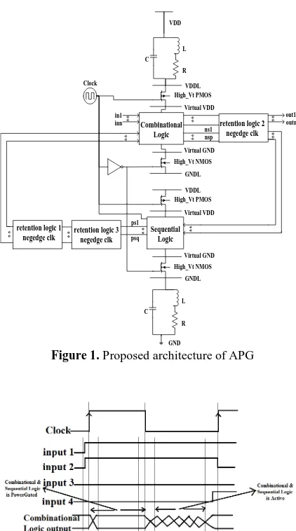
Architecture of new Active Power Gating (APG) approach is shown in Figure 1. This architecture differs from literature [5] in sequential part and data retention part of the design. In this design, both the combinational and sequential blocks are power gated by ST at the positive edge of the clock cycle, whereas reported in literatures [4, 5], only combinational part is power gated. PG of Retention logic is not done for retaining states. Here, PG is applied in the active mode within the clock cycle to minimize the runtime leakage if idle time is present. Three retention logics are used, two of them ('retention logic 1 negedgeclk' (RL1), 'retention logic 2 negedgeclk' (RL2)) are controlled by the negative edge of the clock cycle and
another one ('retention logic 3 posedgeclk (RL3)') is controlled by the positive edge of the clock cycle.
The complete timing diagram of the proposed architecture is shown in Figure 2. During the hold time (Thold) RL1 and RL2 separate the combinational logic from the sequential logic while RL3 passes all the previous states of combinational logic. These states are propagated through the sequential logic and RL1. After hold time, combinational logic and sequential logic are power gated at the remaining part of the positive clock cycle (TPGoff) to reduce leakage power during which no intermediate nodes are passed. At the negative edge of clock cycle (TPGstart), combinational block becomes active and RL3 is turned-OFF. During the evaluation time (Teval), circuit blocks evaluate its state (Teval). After evaluation, RL2 allows the data for evaluation at this stage. Then, the states propagate through the sequential logic and pass through the RL1. During the setup time (Tsetup) inputs change its states. This process is repeated at the next positive edge.
Figure 1. Proposed architecture of APG
Figure 2. Timing diagram of APG architecture VDD
C L
R
High_Vt PMOS VDDL
Virtual VDD
Combinational Logic
High_Vt NMOS Virtual GND
GNDL
High_Vt PMOS VDDL
Virtual VDD
Sequential Logic
High_Vt NMOS Virtual GND
GNDL
C L
R
GND
retention logic 2 negedge clk
retention logic 3 negedge clk retention logic 1
negedge clk Clock
in1 inn
ns1 nsp
out1 outm
ps1
3. NOISE MINIMIZATION APPROACHES
Here, parasitic components: resistance, inductance, and capacitance of the 40-pin Dual In-line Package (DIP-40) [23] assumed in the proposed APG design are 0.217Ω, 8.18nH and 5.32pF respectively for capturing more accurate behavior of the circuit which is not considered in litretures [4, 5]. In this paper, Tri-Mode PG (ckt1), Dual-Switch PG (ckt2), 3-Transistor Controlled PG high VT (ckt3), 3-Transistor Controlled PG low VT (ckt4) approaches are implemented in APG architecture to show the effect of noise on the proposed architecture. A benchmark circuit s27 [24] is taken to implement these architectures. Noise immune designs are simulated and noise results are reported.
4. PROPOSED LOW DROPOUT VOLTAGE REGULATOR (LDO)
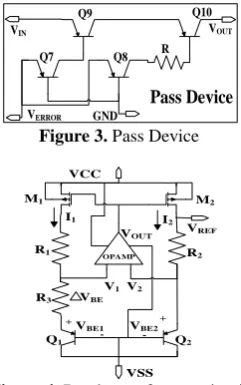
The basic LDO circuit [20] consists of a pass device (PD), ‘voltage reference’ circuit (VR) and error amplifier (EA) with loop control logic. In this work, PD (Figure 3) is implemented with four PNP transistors in Darlington pattern which is quite different from other works. This type of configuration is adopted to generate constant load voltage at high load current with low dropout voltage and low quiescent current for high efficiency. Figure 6 shows the optimized LDO architecture with proposed pass device circuitry that generate desired stable output voltage.
A feedback type bandgap reference circuit (Figure 4) is designed according to the specifications for producing a fixed voltage irrespective of power supply variations, temperature changes and loading on the device. Bandgap circuit produces a fixed voltage by adding a voltage that increases with temperature to a voltage that decreases with temperature. These types of voltage can be generated by tapping the base-emitter voltage (VBE) and using difference in VBE of bipolar junction transistors. In this bandgap circuit, two current components (I1, I2) are generated which are proportional to VEB1 and VEB2. Current mirror by shorting the gates of M1 and M2, is used to force currents into a pair of bipolar transistors whose base emitter voltage difference is used to establish ΔVBE. To create ΔVBE drop at R3, V1 and V2 should be equal. The OPAMP is so designed that the two node voltages V1 and V2 are always equal. Normally for ideal OPAMP, V1 and V2 are always equal as no current flows into the inputs. To make node voltage V1 and V2 equal, the currents I1, I2 and resistors R1, R2 are fixed at an equal value. R3 value should be smaller than R1, R2 to create ∆V𝐵𝐸and temperature incisive of VREF. The current equations of M1 & M2 are:
𝐼1= 𝑘1× (𝑉𝐺𝑆1− 𝑉𝑇1)2 × (1 + 𝜆1× 𝑉𝐷𝑆1) (1)
𝐼2= 𝑘2× (𝑉𝐺𝑆2− 𝑉𝑇2)2 × (1 + 𝜆2× 𝑉𝐷𝑆2) (2)
Pass Device
Q9 Q10
Q8 Q7
GND
VERROR
VIN VOUT
R
Figure 3. Pass Device
VCC
VSS Q2 Q1
R1
R3
R2 M2 M1
OPAMP
VBE
VBE1 VBE2 VREF
V1V2 VOUT
I2 I1
+
-+
-Figure 4. Bandgap reference circuit
where, VGS, VDS, VT and λ are gate to source voltage, drain to source voltage, threshold voltage and channel length modulation parameter respectively. From these two equations of I1 and I2, it is found that:
𝐼2
𝐼1=
𝑘2×(1+𝜆2×𝑉𝐷𝑆2)
𝑘1 ×(1+𝜆1×𝑉𝐷𝑆1) (3)
Here, λ × VDS ≪ 1.
So, we can neglect λVDSfrom the above equation and the new equation will form in the following manner,
𝐼2
𝐼1=
𝐾2
𝐾1 (4)
where, k1 and k2 are aspect ratio. The transistors have been chosen as identical, so the W/L ratio (k) of these two transistors are same, i.e. I1=I2. Current flow through Q1 and Q2 are:
𝐼1= 𝐼𝑠1𝑒
𝑉𝐵𝐸1
𝑉𝑇𝑉 (5)
𝑉𝐵𝐸1= 𝑉𝑇𝑉ln 𝐼1
𝐼𝑠1 (6)
𝐼2= 𝐼𝑠2𝑒
𝑉𝐵𝐸2
𝑉𝑇𝑉 (7)
𝑉𝐵𝐸2= 𝑉𝑇𝑉ln𝐼𝐼2
𝑠2 (8)
since V1=V2=VBE2, if we apply KVL between two transistors Q1 and Q2, the equation will become:
𝑉𝐵𝐸2− 𝐼1× 𝑅3− 𝑉𝐵𝐸1= 0 => 𝐼1=
𝑉𝐵𝐸2-𝑉𝐵𝐸1
𝑅3 =
∆V𝐵𝐸
𝑅3
(9)
where, ∆𝑉𝐵𝐸=𝑉𝑇𝑉ln 𝐼2 x 𝐼𝑆1
𝐼1 x 𝐼𝑆2, VTV=Thermal voltage V1= I1R1,
V2=I2R2, since, V1=V2=> I1R1=I2R2.
Now, apply KVL from VREF node to ground along R3 and Q2 to determine VREF.
VREF = V2+I2R2 (10)
𝑉𝑅𝐸𝐹= 𝑉𝐵𝐸2+
∆V𝐵𝐸
R3 𝑅2 (12)
Hence, the reference circuit produces a temperature incisive voltage as VBE2 decreases and V increases with temperature.
A differential amplifier is used as an EA (Figure 5) to compare the scaled-down version (VSO) of the output (produced by resistors using voltage divider rule) with the fixed reference voltage (VREF). As, proposed PD should be optimized, hence, to drive this device, amplifier is also optimized accordingly. This amplifier is designed using current mirror topology. Current through both the transistors are equal. Sizes of parallel transistors are set as identical (M1=M0, M2=M3, M4=M5) to generate equal amount of current.
The output voltage is maintained by proper design of pass device (PD) and adjusting the ratio of two resistors (R3, R2). The PD must be large enough to guarantee the minimum dropout voltage while providing the maximum load current. The output of the differential amplifier (VERROR) drives the emitter terminal of the two PNP transistors (Q7, Q8). To boost up the current at maximum level, collector terminals of Q7 & Q8 are connected to the base terminals of other two transistors (Q9, Q10) acting as a Darlington pair. Lowest voltage drop is achieved by the voltage across the transistors (Q9, Q10) which is the minimum input-output differential. Here, very low load resistance (R4) is used at the output end. Dropout voltage of the LDO circuit is given by:
VDO = VIN - VOUT
VDO = 2VCE (≈ 250mV for this proposed LDO)
By setting the resistor value (R3, R2), the ‘scaled down voltage (VSO)’ is set and is compared with the fixed reference voltage (VREF). This difference voltage (VERROR = VSO-VREF) drives the PD. When the base-emitter voltage of PNP transistors exceeds 0.6 volts, then base current starts to flow to turn-ON the PD. Output current and the output voltage increases. Again, this output voltage is scaled down and is compared with the reference voltage. Difference of this voltage runs the transistors to increase the output current. After a particular time (VERROR = 0), it enters into the saturation region and constant output current flows, then the output voltage is also fixed.
𝑉𝑆𝑂= 𝑉𝑂𝑈𝑇×
𝑅1
𝑅1+𝑅2 , (13)
when, VERROR = VSO – VREF = 0, then, VSO = VREF:
𝑉𝑂𝑈𝑇= (1 +𝑅𝑅2
1) × 𝑉𝑅𝐸𝐹 (14)
Equation (14) is true when VIN is sufficiently high to keep differential amplifier and pass device in saturation region. In this region, VOUT becomes constant which set VDO to very low voltage.
As part of its regulation, differential amplifier and bandgap reference circuit of LDO can attenuate any spikes in the input voltage which have some deviation from the internal reference.
VDD
VSS
M1
M2
M4
M0
M3
M5
V2
V1
Idc = 0
VOUT
Figure 5. Error amplifier (EA) circuit
PASS DEVICE
Error Amplifier
Bandgap Reference Circuit
VCC
GND
VREF
VOUT VIN
VERROR
VSO R3
R2
R4 C13
Figure 6. Proposed LDO architecture
High PSRR LDO can be generated by minimizing dropout voltage. So, spikes on power rail can be suppressed by using the high PSRR LDO in the circuit. If LDO regulator is used in the power line of PG architecture, then only this device can regulate fluctuated supply voltage during PG mode. It can also help the neighboring circuits to function correctly while sharing the same power line.
5. PROPOSED NOISE MINIMIZATION SCHEME USING LDO IN APG ARCHITECTURE
In this paper, this architecture implemented considering package inductance is termed as ckt5 (Figure 7). The proposed LDO regulator is attached between the high_VT transistor (ST) and the power rail (VDDL) in APG architecture.
Noise on power rail can be defined by:
∆𝑉 = (𝑉𝐷𝐷− 𝑉𝐷𝐷𝐿) ≅ 𝐿 𝑑
𝑑𝑡𝐼(𝜉, 𝑡), (15)
where,ξ=(VDD-VDDL), VDD = supply voltage, VDDL= voltage drop at power rail.
During mode transition of PG circuit, voltage drops on power rail due to the flow of high current leads to increase in noise (ΔV = VDD - VDDL). To overcome this problem, high PSRR with low dropout LDO regulator is proposed and implemented in the PG circuit that can reject spikes on the power rail (VDDL) using its internal differential amplifier, bandgap reference circuit and pass device. LDO reduces variation on the power rail (VDDL) by regulating the voltage of VDDL node. This in turn increases the value of VDDL node near to VDD. Hence, noise (ΔV=VDD - VDDL) on the power rail reduces which leads to decrease in the rate of change of current (𝑑
𝑑𝑡𝐼(𝜉, 𝑡)) flow
VDD
C
L R
VDDL
Combinational Logic
High_Vt NMOS Virtual GND GNDLDO
Sequential Logic
C
L R GND Clock
in1 inn
ns1 nsp
out1 outm
ps1 psq
High_Vt NMOS
GNDL Virtual GND High_Vt PMOS
Virtual VDD
VDDLDO High_Vt PMOS
Virtual VDD
LDO
VDDLDO
LDO
GNDLDO
Figure 7. A scheme of using LDO regulator in APG (ckt5)
6. SIMULATION RESULT
The designs of proposed modified APG and ckt1, ckt2, ckt3, ckt4, ckt5 and LDO are implemented taking benchmark circuit- s27. It is observed from Table 1, that with the reduction of the frequency of operation as idle time increases, APG design becomes more efficient to reduce leakage. Power saving results of this APG design outperforms the results of the previous PG works [3, 4, 25-27]. Memory access PG reduces the wasted core leakage power by 38.04% [26]. For 16-bit multiplier design at frequency 1MHz, power saving is 29% compared to PG design [4]. Data-Retained PG (DRPG) [27] used to reduce active mode leakage achieves up to 25.7% saving over conventional designs.
At 2.5V input voltage, output and dropout voltage of the proposed LDO is 2.00253V and 247.47mV respectively. This regulator produces load current of 50.3343mA and the quiescent current of 117.79μA. The measured PSRR is as high as 73.97dB with an efficiency of 88.79%.
LDO maintains around 250mV dropout voltage in between 2-3V input voltage and plot of line regulation is shown in Figure 8.
It is also seen that LDO maintains output voltage of about 2.3V with the variation of input voltage from 2.25 – 2.75V (Figure 9).
TABLE 1. Percentage saving of power over no PG
Frequency (MHz)
%Saving in Average Power of APG over no
PG
%Saving in Leakage of APG
over no PG
f=1.25 54.78 86.83
f=1.67 17.81 68.33
f=2.50 10.63 47.33
The variation of output voltage with the changes of load current from 30 to 50mA is shown in Figure 10. The load regulation of the proposed LDO is observed to be 2.28%. This proposed LDO provides output voltage of about 2V by varying the load resistance (R4) from 30Ω to 100Ω. It is shown that, output voltage is almost constant at higher load resistance (5 - 10KΩ) as shown in Figure 11.
The variation in output voltage with respect to temperature is also observed for the proposed LDO circuit (Figure 12). From the Figure 12, it is seen that output voltage becomes constant after room temperature attainment for the proposed LDO circuit. Then, bounce noise produced by the ckt1, ckt2, ckt3, ckt4, ckt5 in PG circuit during sleep to active mode is discussed.
Figure 8. Output voltage Vs input voltage
Figure 9. Transient response of voltage
Figure 10. Output voltage Vs load current
Figure 11. Output voltage Vs load resistance
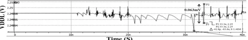
From Table 2, it is observed that noise on the power supply (0.06mV) in ckt5 is lower than the ckt1, ckt2, ckt3, ckt4 over APG. There is a large deviation in the voltage level of power supply with package inductance in APG. Whereas, there is less peak to peak variation in power rail with the noise reduction logic of the PG circuits. Percentage saving of noise (peak to peak variation) over APG is also shown in Figure 13.
Percentage saving of noise on the power rail in ckt5 is 98% compared to the ckt1, ckt2, ckt3, ckt4. Transient analysis of peak to peak noise produced on the power rail using LDO regulator for ckt5 is shown in Figure 14. From Table 3, it is found that, proposed noise reduction approach gives better result compared to other previous works. Using proposed concept voltage fluctuation reduces significantly, but power and area occupancy increases due to the extra circuit component of LDO.
TABLE 2. Peak to Peak Noise on Power Rail over APG Peak to Peak Noise on Power Rail (mV)
APG Ckt1 Ckt2 Ckt3 Ckt4 Ckt5
2.69 2.23 1.5 2.4 1 0.06
Figure 13. Saving of Noise on Power Rail over APG
Figure 14. Peak to peak noise on power rail for ckt5
TABLE 3. Noise reduction comparison with previous work
[7] [12] [13] [15] Proposed
Work
Noise reduction
(%) 30-74 63.93 94.16 76.28 99
7. CONCLUSION
In this paper, a new PG architecture is proposed for minimization of noise and power. PG is applied for both the combinational and sequential block in active mode. But, PG circuit also suffers from noise on the power rail during sleep to active mode. Effectiveness of different noise reduction approaches in this proposed architecture have also been analyzed in this paper. All the circuits - APG, ckt1, ckt2, ckt3, ckt4, ckt5 have been designed for reduction of noise on the power supply. Peak to peak voltage fluctuation is reduced more in this scheme of using low dropout voltage regulator in PG architecture compared to the other approaches.
8. ACKNOWLEDGEMENT
This work is supported by SMDP-C2SD project, sponsored by MeitY, Govt. of India.
9. REFERENCES
1. Giacomotto, C., Singh, M., Vratonjic, M. and Oklobdzija, V.G., “Energy Efficiency of Power-Gating in Low-Power Clocked Storage Elements”, Lecture Notes in Computer Science, Vol. 5349, (2009), 268-276.
2. Leverich, J., Monchiero, M., Talwar, V., Ranganathan, P. and Kozyrakis, C., "Power management of datacenter workloads using per-core power gating", IEEE Computer Architecture
Letters, Vol. 8, No. 2, (2009), 48-51.
3. Pakbaznia, E. and Pedram, M., "Design and application of multimodal power gating structures", in Quality of Electronic Design, 2009. ISQED 2009. Quality Electronic Design, IEEE., (2009), 120-126.
4. Mistry, J.N., Al-Hashimi, B.M., Flynn, D. and Hill, S., "Sub-clock power-gating technique for minimising leakage power during active mode", in Design, Automation & Test in Europe Conference & Exhibition (DATE), 2011, IEEE., (2011), 1-6. 5. Nath, D., Choudhury, P., Nag, A. and Pradhan, S.N., "Power
gating architecture implementation inside clock period to reduce power", International Journal of Computer Aided Engineering
and Technology 5, Vol. 6, No. 3, (2014), 310-323.
6. Kim, S., Choi, C.J., Jeong, D.-K., Kosonocky, S.V. and Park, S.B., "Reducing ground-bounce noise and stabilizing the data-retention voltage of power-gating structures", IEEE transactions
on Electron Devices, Vol. 55, No. 1, (2008), 197-205.
7. Singh, R., Kim, A., Kim, S. and Kim, S., "A three-step power-gating turn-on technique for controlling ground bounce noise", in Proceedings of the 16th ACM/IEEE international symposium on Low power electronics and design, ACM., (2010), 171-176. 8. Singh, R., Woo, J.-K., Lee, H., Kim, S.Y. and Kim, S.,
"Power-gating noise minimization by three-step wake-up partitioning", 17%
40.89%
7.80% 62.82%
98%
0% 50% 100%
IEEE Transactions on Circuits and Systems I: Regular Papers, Vol. 59, No. 4, (2012), 749-762.
9. Kumar, Y., Paliwal, S., Rai, C.K. and Balasubramanian, S., "A novel ground bounce reduction technique using four step power gating", in Engineering and Systems (SCES), 2013 Students Conference on, IEEE., (2013), 1-5.
10. Kim, S., Kosonocky, S.V., Knebel, D.R., Stawiasz, K. and Papaefthymiou, M.C., "A multi-mode power gating structure for low-voltage deep-submicron cmos ics", IEEE Transactions on
Circuits and Systems II: Express Briefs, Vol. 54, No. 7, (2007),
586-590.
11. Chowdhury, M.H., Gjanci, J. and Khaled, P., "Controlling ground bounce noise in power gating scheme for system-on-a-chip", in Symposium on VLSI, 2008. ISVLSI'08. IEEE Computer Society Annual, IEEE., (2008), 437-440.
12. Jiao, H. and Kursun, V., "Ground-bouncing-noise-aware combinational mtcmos circuits", IEEE Transactions on Circuits
and Systems I: Regular Papers, Vol. 57, No. 8, (2010),
2053-2065.
13. Jiao, H. and Kursun, V., "Ground bouncing noise suppression techniques for data preserving sequential mtcmos circuits", IEEE
Transactions on Very Large Scale Integration (VLSI) Systems,
Vol. 19, No. 5, (2011), 763-773.
14. Saxena, C., Pattanaik, M. and Tiwari, R., "Enhanced power gating schemes for low leakage low ground bounce noise in deep submicron circuits", in Devices, Circuits and Systems (ICDCS), 2012 International Conference on, IEEE., (2012), 239-243.
15. Sreenivasulu, P. and Rao, K.S., "Ground bouncing noise reduction in combinational mtcmos circuits", in Communication and Network Technologies (ICCNT), 2014 International Conference on, IEEE , (2014), 270-275.
16. Talwekar, R. and Jain, N.B., "Enhanced ground bounce noise reduction in low leakage cmos multiplier cell", in Research Advances in Integrated Navigation Systems (RAINS), International Conference on, IEEE., (2016), 1-6.
17. Kumar, Y., Paliwal, S., Sahu, P. and Balasubramanian, S., "Ground bounce noise minimization using multi-vdd level converter", in Electronics, Computing and Communication
Technologies (IEEE CONECCT), 2014 IEEE International Conference on, IEEE., (2014), 1-4.
18. Wu, Q., Li, W., Li, N. and Ren, J., "A 1.2 v 70 ma low drop-out voltage regulator in 0.13 µm cmos process", in ASIC (ASICON), 2011 IEEE 9th International Conference on, IEEE., (2011), 978-981.
19. Hicham, A. and Qjidaa, H., "A 500μa low drop-out voltage regulator in 90-nm cmos technology", in Complex Systems (ICCS), 2012 International Conference on, IEEE., (2012), 1-4. 20. Kugelstadt, T., "Fundamental theory of pmos low-dropout
voltage regulators", Texas Instruments Application Report, (1999), 1-6.
21. Giustolisi, G., Palumbo, G. and Spitale, E., "Robust miller compensation with current amplifiers applied to ldo voltage regulators", IEEE Transactions on Circuits and Systems I:
Regular Papers, Vol. 59, No. 9, (2012), 1880-1893.
22. Torres, J., El-Nozahi, M., Amer, A., Gopalraju, S., Abdullah, R., Entesari, K. and Sanchez-Sinencio, E., "Low drop-out voltage regulators: Capacitor-less architecture comparison", IEEE
Circuits and Systems Magazine, Vol. 14, No. 2, (2014), 6-26.
23. Kim, S., Kosonocky, S.V. and Knebel, D.R., "Understanding and minimizing ground bounce during mode transition of power gating structures", in Proceedings of the 2003 international symposium on Low power electronics and design, ACM., (2003), 22-25.
24. ISCAS89. Sequential benchmark circuits.
25. Lee, B.S., "Technical review of low dropout voltage regulator operation and performance", Application Report... slva072, (1999).
26. Jeong, K., Kahng, A.B., Kang, S., Rosing, T.S. and Strong, R., "Mapg: Memory access power gating", in Proceedings of the Conference on Design, Automation and Test in Europe, EDA Consortium., (2012), 1054-1059.
27. Kahng, A.B., Kang, S. and Park, B., "Active-mode leakage reduction with data-retained power gating", in Proceedings of the Conference on Design, Automation and Test in Europe, EDA Consortium., (2013), 1209-1214.
Low Dropout
Based Noise Minimization of Active Mode Power Gated Circuit
D. Nath, S. N. Pradhan
Department of Electronics & Communication Engineering, National Institute of Technology Agartala, Agartala, India
P A P E R I N F O
Paper history: Received 14 August 2016
Received in revised form 02 December 2017 Accepted 04 February 2018
Keywords: Architecture Power-gating Data-retention Leakage Noise Low-dropout Voltage هديكچ
اقلا هتسب روضح یی
ا ثعاب داجی ون سناب( لااب ژاتلو ناسون زی
ط رد ) ی تنا ق اپ هب لااب ناوت لا نیی
ور رب ی ر لی گ رادم رد تردق تی
م تردق ی هک دوش
غت تسا نکمم تاریی
اهرادم رد ار هتساوخان ی
ا رواجم داجی ا رد .دنک نی راک کی حارط ی گ تی ارب تردق ی وت لاعف تلاح رد ناوت شهاک هعس
ون .تسا هدش هداد زی ن زی ارب ی ا نی حارط ی لحت لی ثأت .تسا هدش ری شور اه ی ون شهاک فلتخم زی ارب ی ون شهاک زی ذغت عبنم هی حارط رد ی گ تی زرا تردق یبای ا رد .تسا هدش نی
،هلاقم کی دج موهفم دی مک شور زا هنی زاس ی ون زی جورخ ژاتلو روتلاوگر زا هدافتسا اب ی اپ نیی پ داهنشی .تسا هدش اش رادقم ژر هرگ رد اه ی لخاد ی رط زا هک قی زنارت روتسی ب زا رذگ لوط رد باوخ یرادی
م روبع ی نکت طسوت ،دنک کی اه ی مک هنی زاس ی ون زی پ داهنشی
اپ ژاتلو روتلاوگر .تسا هدش لرتنک هدش نیی
جورخ ی ون شهاک فده اب زی
رط زا رواتشگ قی ور رب ژاتلو تاناسون ندناسر لقادح هب ی ر لی تردق ارط ح ی سا هدش ت حارط . ی اه ی گ تی ون و لاعف تلاح رد تردق زی
رازبا طسوت مک Synopsys Custom Designer
ژولونکت رد ی 90 nmiPDK
حارط ی هدش هفرص .دنا وج یی ون رد زی ر رد لی ذغت عبنم هی ات 99 ٪ هدهاشم هدش .تسا