© 2014, IJCSMC All Rights Reserved
840
Available Online atwww.ijcsmc.comInternational Journal of Computer Science and Mobile Computing
A Monthly Journal of Computer Science and Information Technology
ISSN 2320–088X
IJCSMC, Vol. 3, Issue. 10, October 2014, pg.840 – 844
RESEARCH ARTICLE
IMPLEMENTATION OF LOW POWER
LOW NOISE PROBABILISTIC-BASED
LOGIC DESIGNS
Dhanasekaran.S
1, Ragavi.N
2, Yamini.E
3¹Department of ECE, Anna University, India ²Department of ECE, Anna University, India ³Department of ECE, Anna University, India
1
[email protected]; 2 [email protected]; 3 [email protected]
Abstract- In this paper an ultra-low power and probabilistic based noise tolerant latch is proposed based on Markov Random Field (MRF) theory. The absorption laws and H tree logic combination techniques are used to reduce the circuit complexity of MRF noise tolerant latch. The cross coupled latching mechanism is used at the output of the MRF latch In order to preserve the noise tolerant capability of MRF latch. The proposed latch is faster than the latches presented in the literature and provides low power and high noise immunity. Hence we can achieve good trade off in terms of performance, robustness and cost. The latches are evaluated in 180nm CMOS technology. The results obtained show that the proposed latch consumes low power and highly noise tolerant. Finally the proposed latch is applied in transmission gate based full adder circuit. In 180nm technology the proposed adder can operate reliably with superior noise tolerance and low power compared to conventional latch based full adder circuit.
Keywords- Markov Random Field (MRF) latch, Markovian Property, C-element, Single Event Upset (SEU), Soft error tolerant, Root Mean Square (RMS) noise voltage
I.
INTRODUCTION© 2014, IJCSMC All Rights Reserved
841
[4], while trying to meet all the other constraints imposed on the design. However, lowering supply voltage also increases circuit delay and degrades the drivability of cells designed with certain logic styles. The lower threshold voltage will cause a decrease in noise-tolerance. Moreover, noise does not scale down proportionally as supply voltage decreases. As the size of CMOS devices continues to scale down to the nanometer scale, signal errors caused by noise can significantly affect the circuit performance. The circuits operate at low noise margins and thus VLSI circuits are more sensitive to noise [1-3]. The MRF approach is further extended to the design of a probabilistic-based noise-tolerant sequential circuit in this paper.
II.
SEQUENTIAL CIRCUITSSequential circuits are classified into latches and flip-flops, where flip-flops are edge triggered sequential circuits and latches are level sensitive sequential circuits. When the noise affects the input signal, the latch will be affected during the entire transparent period while the flip-flop will be affected during the clock transition edge. Hence, the latches are mostly affected by noise than flip-flops. Hence, latches are inherently more susceptible to noise interference. In order to minimize the effect of noise interference and allow the circuit to operate reliably under low-voltage, low power, and low-SNR environments, we propose a noise-tolerant latch design by using Markov Random field (MRF) theory [1].
A. Mux Based Latch Circuits
In the Multiplexer-based latch, MUX-Latch [1], the CLK signal acts as the switch. When CLK is at logic low, the latch is in latching mode and its output remains unchanged. When CLK is at logic high, the latch circuit enters into transparent mode, where its output logic state is determined by its input signal [6]. The noise interference at the input affects the correctness of the output state when the latch is in the transparent mode. The circuit complexity is less but requires more transistors and delay is more. In two transmission Gate-Latch the charging and discharging period is reduced as the clk frequency increases. In the transmission gate cross- coupled feedback inverter latch [1], the operational speed is slightly increased and the power consumption is slightly reduced. The main drawback is when the input is switching in the transparent mode, the contention between the feedback signal and the feed forward input signal will cause additional operational delay and more power consumption.
B. Soft Error Tolerant Latch Designs
The soft errors are due to internal and externally induced phenomena such as a particles and cosmic rays in adverse environments during system operation; this is especially deleterious for storage elements, such as flip-flops, latches. To reduce the impact of a soft error on latches, hardening techniques have been utilized. Soft-error tolerant latch designs with increased soft error upset tolerance capability such as Feedback Redundant SEU-Tolerant Latch (FERST),Split Internal Low Cost latch[4] (SIN-LC) and HiPeR latch design [5] are discussed . These latest designs can perform with superior noise tolerance for soft-error. Since soft errors are usually one shot noise they cannot resist continuous noise interference which leads to the destruction of the C-element. As a result, for the noise interference with multiple error cases, the output or of these latch designs may be malfunction. The hardware complexities of these latch designs are usually higher, as more transistors are required for the construction of the C-element.
III.
MARKOV RANDOM FIELD (MRF) THEORY
© 2014, IJCSMC All Rights Reserved
842
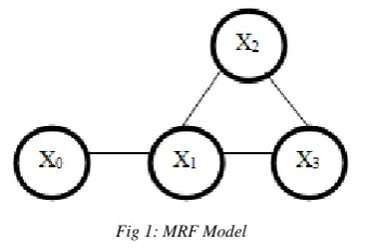
Fig 1: MRF ModelAn appropriate model for the MRF is a graph structure, where the nodes of the graph represent logic variables and the edges represent statistical dependency between the variables. An example of such a graph is shown in Figure 1 for a very small logic circuit. There are four logic variables represented by the vector {x0, x1, x2, x3} and these variables are the nodes of the graph in the lower half of the Fig.1. The edges of the graph indicate that the subsets of nodes {x0, x1},{x1,x2,x3} directly interact. These subsets are called cliques from the graph theory concept of node subsets that are all mutually connected by graph edges [7]. For any MRF graph G there exists a set of cliques C that represent the local statistical dependencies of logic states. The distribution of noise energy can be spread and shared among these MRF neighboring nodes[9-12]. The noise-tolerant capability is achieved in a MRF network through iteratively updating the logic states of each individual node. Ultimately the network converges to a stable set of state, which corresponds to the correct logic states of each node. It is worth mentioning that successful operation in an MRF network model only requires that the energy of correct states is lower than the energy of incorrect states which can therefore easily be achieved. In[7] the hardware complexity in constructing an MRF logic gate is reduced through Boolean simplification and valid minterm reduction. Mapping the MRF logic gate by using the simplified Boolean equation in the circuit can greatly reduce the area.
A. Markov Random Field (MRF) Latch
Based on this idea, MRF latch was designed with low power and high noise immunity. The circuit complexity is reduced using absorption law and H tree balanced logic circuit merging method[13-15]. After H-tree combination these cascaded logical gates with the same type, will lower the influence of noise in each MRF network node and reduce the current charging/discharging paths. It is beneficial to enhance both noise tolerance and power consumption. With the cross- coupled latching mechanism design, the conduction of transistors will become a collaborative decision together with the two added transistors n1 and n2 and no longer be reliant on only a single transistor. The conduction of transistors n1 and n2 are decided by the complementary cross coupled feedback signals, the possibility of direct conduction of the transistors is greatly reduced [1].This results in the reduction of noise tolerance and power consumption in MRFlatch .When CLK=1, the latch circuit is in transparent mode, where the latch’s output Q is directly determined by its input D. When CLK = 0, the latch circuit is in latching mode, where the latch’s output Q is latched the same as its previous state Q2. The operation mode of a latch is mainly controlled by the CLK signal.
© 2014, IJCSMC All Rights Reserved
843
IV.
RESULTS AND COMPARISIONThe Table.1 exhibits performance of all the existing latches and proposed latch in terms of delay, area and power, RMS noise voltage. The results show that the proposed MRF latch provides better noise tolerance and low power compared to the existing latches.
TABLE 1
.PERFORMANCE OF THE PROPOSED MRF LATCH COMPARED WITH PREVIOUS IMPLEMENTATIONS
LATCH POWER AREA DELAY RMS INPUT NOISE
VOLTAGE
RMS OUTPUT NOISE VOLTAGE
MUX based latch
3.116nw 377 µm2 3.000 ps 34.732V 42.739V
TG based mux latch
2.833uw 273 µm2 207.95ps 35.812V 48.066V
TG cross Coupled latch
8.112uw 276 µm2 366.60ps 35.313V 39.049V
FERST latch 5.639nw 780 µm2 9.8711ps 29.756V 30.498V
Sin-LC latch 10.759nw 216 µm2 64.471ps 36.678V 38.408V
Hiper latch 282.91uw 546 µm2 10.303ps 32.921V 33.140V
MRF latch 0.9487nw 588 µm2 662.31ps 41.427V 23.603V
V.
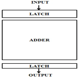
APPLICATION OF THE LATCH IN FULL ADDER CIRCUITAddition is one of the fundamental arithmetic operations and is used extensively in many VLSI systems. In most of these systems, the adder is part of the critical path that determines the overall performance of the system and the full adder is the core element of complex arithmetic circuits. In most of the digital systems adder lies in the critical path that increases the overall computational delay of the system [8]. Around 30% of the total power is consumed by the data path. Adders are an extensively used component in data path and therefore careful design and analysis is required. The overall system performance can be increased significantly by enhancing the performance of the full adders. In order to reduce the delay in adder circuit latches are used at input and output as shown in Fig.3. In many digital applications the values need to be stored .In that case latches are used to store the values. Later the values can be fetched for future use. The existing latches and proposed latches in full adder circuit are compared in terms of power, area, delay and noise The Table II shows the comparison of all these parameters.
© 2014, IJCSMC All Rights Reserved
844
The delay is decreased slightly but the area overhead is more. The proposed MRF latch in full adder circuit operates at low power compared to the conventional designs.
VI.
CONCLUSIONIn this paper a low power noise tolerant Markov Random Filed latch design is proposed. In TSMC 180 nm CMOS process, the proposed circuit can operate reliably under low power and superior noise tolerance as compared with the conventional CMOS latch design. Through MRF mapping decomposition, MRF theory is applied to sequential noise tolerant circuits. By applying the absorption law and H-tree logic combination techniques to simplify MRF noise-tolerant latch circuit, the circuit complexity and power consumption was reduced. By applying the cross-coupled latching mechanism in the output of MRF latch, the noise tolerance of MRF latch was preserved. Hence the Markov Random Field (MRF) latch consumes low power and highly noise tolerant compared to all the existing latches. Finally, the MRF latch is implemented in full adder circuit. In adder circuit the Markov Random Field (MRF) latch consumes low power and highly noise tolerant compared to the existing latches implemented in full adder circuit. In future the proposed MRF latch will be applied in Digital signal processing applications like multipliers, memories.
REFERENCES
[1] I-Chy Wey, Yi- Jung Lan, Chien-Chang Peng “Reliable Ultra Low voltage low power probabilistic- based noise
tolerant latch design”,Elsevier Microelectronics Reliability June 2013.p.1-6
[2] Wey IC, Chen YG, Yu CH, Chen J, Wu AY. “A 0.13 lm hardware-efficient probabilistic- based noise tolerant circuit
design and implementation with 24.5 dB noise-immunity improvement”. In: Proceeding of IEEE Asian solid-state circuits
conferences; November 2007. p. 316–9.
[3] Wey IC, Chen YG, Yu CH, Chen J, Wu AY. “A 0.18 lm probabilistic -based noise tolerant circuit design and
implementation with 28.7 dB noise-immunity improvement”. In: Proceeding of IEEE Asian solid-state circuits
conferences; November 2006. p. 291–4.
[4] Omana M, Rossi D, Metra C. “ Latch Susceptibility to Transient faults and New Hardening Approach” IEEE Trans on
Computer Sept.2007;p.1255-68.