ORIGINAL RESEARCH ARTICLE
EFFECT OF SUBSTRATE TEMPERATURE ON OPTICAL AND ELECTRICAL PROPERTIES
OF CdZnSeTe THIN FILMS PREPARED BY SPRAY PYROLYSIS TECHNIQUE
1*
Gaikwad, S. A.,
2Tembhurkar, Y.D. and
3Dudhe, C.M.
1
Department of Physics, Guru Nanak Science College, Ballarpur (M.S.)-442701
2
Department of Physics, S. K. Porwal College, Kamptee-441002
3
Department of Physics, Institute of Science, Nagpur-440001
ARTICLE INFO ABSTRACT
Polycrystalline semiconducting chalcogenide thin films of CdZnSeTe are prepared on large area of glass substrate by spray pyrolysis technique. Thin films of CdZnSeTe deposited at different substrate temperatures 250°C, 275°C, 300°C and 325°C were investigated. Absorption coefficients for the films were evaluated from optical transmission spectra in the wavelength range 350nm-1100nm.Composition was confirmed from EDAX while SEM pictures shows the presence of nanotubes. Graphs plotted between (αhν)2 and(hν) yields straight lines indicating
direct transition with optical band gap energies in the range 2.40eV- 2.44 eV. Optical properties such as extinction coefficient, refractive index and dielectric constant have been evaluated in wavelength range 350nm-1100nm. Electrical study was carried out by four probe method. Arrhenius behavior shows semiconducting nature of the films Values obtained by this method are found to be suitable to use the thin films for many scientific and technical applications such as solar cells, heat mirrors detectors etc.
Copyright ©2017,Gaikwad et al. This is an open access article distributed under the Creative Commons Attribution License, which permits unrestricted use, distribution, and reproduction in any medium, provided the original work is properly cited.
INTRODUCTION
Cadmium and zinc based II–VI wide-bandgap compound semiconductors have potential applications for various opto-electronic devices as well as x-ray and γ-ray detectors
(Sebastian, 1989; Matsumura, 2003; Noda et al., 2000; Feng et
al., 1994). In addition to applications such as opto-electronic
devices and x-ray/ γ-ray detectors, Cd-based binary compounds grown on Si, such as CdTe/Si, have been used as composite substrates for HgCdTe material, an infrared (IR)
detecting semiconductor system (Chen et al., 1993; Wang,
1995; deLyon, 1994; Wijewarnasuriya et al., 1998; Brill et al.,
2001; Dhar et al., 1996). Similarly, ternary alloys, such as
CdZnTe/Si and CdSeTe/Si, as well as quaternary compounds, such as CdZnSeTe/Si, can also be used as composite substrates specifically engineered for exact lattice matching with HgCdTe material designed to detect in the long wavelength IR region Various methods have been used to prepare CdZnSeTe
*Corresponding author: Gaikwad, S. A.,
Department of Physics, Guru Nanak Science College, Ballarpur (M.S.)-442701.
thin films such as molecular beam epitaxy (Dinan, 1985), liquid phase epitaxy (Pellicary, 1988), electrode position
(Basol et al., 1989), spray pyrolysis(Tembhurkar. 2016,
2017)close space vapour transport (Gonzales-Hernandes et al.,
1991), laser ablation (Aydinly, 1991), thermal vapour
evaporation (Kim et al., 2004), sputtering (Becerril, 2004) and
metal–organic chemical vapour deposition (MOCVD)( Chu, 1992).
Experimental details
Preparation of samples
Aqueous solutions of cadmium chloride, zinc chloride, selenium dioxide and tellurium tetrachloride were mixed in the ratio1:1:3.2:3.2 by volume for spraying. The molarity of each solution was 0.02M and chemicals used were of AR grade. The films deposited have selenium and tellurium deficiencies if the ratio of solution is 1:1:2:2. The excess selenium and tellurium are used to remove these deficiencies (Tembhurkar, 1992).
ISSN: 2230-9926
International Journal of Development Research
Vol. 07, Issue, 12, pp.17771-17775, December,2017
Article History:
Received 16th September, 2017
Received in revised form 21st October, 2017
Accepted 09th November, 2017
Published online 29th December, 2017
Key Words:
Thin films, CdZnSeTe, Spray Pyrolysis, Optical Constants, Band gap Energy.
Citation: Gaikwad, S. A., Tembhurkar, Y.D. and Dudhe, C.M. 2017. “Effect of substrate temperature on optical and electrical properties of CdZnSeTe
thin films prepared by spray pyrolysis technique”, International Journal of Development Research, 7, (12), 17771-17775.
The temperature of substrate which are in the form of double washed and then heated biological glass plates. The temperature of the substrate was maintained at 300°C and was measured by a pre-calibrated copper constantan
thermo-couple. The solution was sprayed at a pressure of 12 Kg/cm2.
The glass sprayer was mechanically moved to and fro during spraying to avoid the formation of droplets on the hot substrate and ensure instant evaporation. The spray rate was maintained at 3.5 ml/min. The thickness of the films was measured by weighing method and Michelson interferometer. The only difference between these two methods is of the order of 0.003μm. Transmission was taken on UV-1800 Shimadzu spectrophotometer in the wavelength range 350nm-1100nm. Electrical conductivity was measured by four probe method. Chemical composition analysis of the film was tested by EDAX analysis. The surface morphologies of as deposited CdZnSeTe thin films were carried out by scanning electron microscope.
RESULTS AND DISCUSSION
Optical studies
Optical band gap: The Optical transmission spectra of as
deposited CdZnSeTe thin films was taken with the help of UV-1800 Shimadzu spectrophotometer in the wavelength range
350nm-1100nm. Fig.1. shows the resultant optical
transmission spectra of as deposited CdZnSeTe thin films at substrate temperatures 250°C, 275°C, 300°C and 325°C. For the calculation of absorption coefficient (α) at various wavelengths the method used by Rubin et.al.(1986) was adopted.
Fig.1.Transmission spectra of as deposited CdZnSeTe thin films at substrate temperatures a)250°C, b)275°C, c)300°C and
d)325°C
For the sample of thickness t
’
, α is given by the relation,
α = ( 1/t) ln(I0 /I), (1)
where I0 and I are the intensities of incident and transmitted
radiations respectively. Absorption coefficient is also related to % transmittance by the relation,
α = ( 1/t) ln(1/T) (2)
Where ‘T’is the optical transmittance.
The optical study shows that the as deposited films are absorptive having high absorption coefficient. Optical band
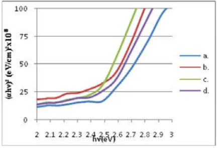
gap can be determine from the graph between (αhᴠ)2 and
[image:2.595.326.545.93.240.2](hᴠ)and extrapolating the graph on (hᴠ)axis as shown in fig.2.
Fig.2.Variation of(αhν)2 as a function of photon energy(hν)of as deposited CdZnSeTe thin films at substrate temperatures
a) 250°C, b)275°C, c)300°C and d)325°C
[image:2.595.315.555.431.560.2]The values of optical band gap energies for as deposited Cd Zn Se Te thin films at different substrate temperatures are listed in table 1.The linearity of graphs in high energy region indicate direct type of transitions in the films. It is observed that optical band gaps of CdZnSeTe decreases from 2.44eV to 2.40 eV as substrate temperature increases from 250°C to 300°C which is due to increase in grain size with increase in substrate temperature and beyond 300°C, the optical band gap again increases with increase in substrate temperature as shown in fig.3 These results are found to be in good agreement with that
[image:2.595.53.279.437.590.2]obtained by Umeshkumar et al. and Murali et al. (2011-2009).
Fig.3 Variation of optical band gap with substrate temperature for as deposited CdZnSeTe thin films
Extinction coefficient and refractive index
The extinction coefficient ‘k’ is related to absorption
coefficient ‘α’ by the relation (Coutts et al., 2001,. Mahrov et al., 2004, Mahrov et al., 2004).
K = α λ / 4 π (3)
Refractive index
‘
n
’
for the film is calculated using the relation,
n = (1 + √R)/(1 - √R ) (4)
where ‘α’ is the absorption coefficient , ‘λ’ the wavelength and
‘
R’ the reflectance. The calculated values of extinction
Real and imaginary parts of dielectric constant
The real (ε1) and imaginary(ε2) parts of dielectric constant are
[image:3.595.309.554.49.200.2]given by the relations (Abd El-Wahabb, 2001).
Fig.4. Variation of extinction coefficient with wavelength(nm)for as Deposited CdZnSeTe thin films at substrate temperatures a)
[image:3.595.45.284.106.242.2]250°C, b)275°C, c)300°C and d)325°C
Fig. 5. Variation of refractive index as a function of wavelength for as deposited CdZnSeTe thin films atsubstrate temperatures a)
250°C b)275°C c)300°C d)325°C
ε1 = n2 – k 2 (5)
ε2 = 2nk (6)
We also calculated real and imaginary parts (ε1 and ε2)of
dielectric constants at several wavelengths ranging from 350 nm-1100nm as it is directly related to the density of states within the energy gaps of the films. Fig 6 and 7 shows the variation of real and imaginary parts of dielectric constant for CdZnSeTe thin films at substrate temperatures 250°C, 275°C,300°C and 325°C respectively.
Fig. 6. Variation of real part of dielectric constant of CdZnSeTe films at substrate temperatures a)250°C b)275°C c) 300°C,
[image:3.595.55.272.291.435.2]d) 325°C
Fig. 7. Variation of imaginaryl part of dielectric constant of CdZnSeTe thin films at substrate temperatures a)250°C
b)275°C, c) 300°C, d) 325°C
It is observed from the graph that both real and imaginary parts of dielectric constant decreases with increasing wavelength.
The nature of curves for both ε1 andε2 are found to be same,
the only difference is that the values of real parts are higher than those of imaginary parts.
SEM studies
Surface morphology of thin films can be studied with the help of SEM analysis.Fig.9 shows the SEM picture of as deposited CdZnSeTe thin films at substrate temperature 300°C which shows the presence of nanotubes.
Electrical stuies
The conductivity of CdZnSeTe thin films was measured by four probe method. The Arrhenius plots of conductivity for as deposited CdZnSeTe thin films deposited at substrate temperatures 250°C,275°C,300°C are shown in fig.8.Figures shows that conductivity increases with increase increasing substrate temperatures.The higher values of conductivity may
be due to higher crystalinity (Garadkar et al., 2010). Plots
again shows that there are two distinct conductivity regions indicating more than one conduction mechanisms due to localized states responsible for this conduction process are the direct consequences of imperfections associated with thin films (More, 2003). The activation energies in two regions were calculated using the relation,
[image:3.595.314.556.570.744.2] [image:3.595.46.281.600.753.2]Fig.9 SEM image of as deposited CdZnSeTe thin film films at substrate temperatures 300°C.
σ=σ0 exp (-Ea/kT) (7)
where ‘k’ is Boltzman constant, ‘σ’ is conductivity of thin film
at temperature T, ’σo
’
is a constant and ‘Ea
’
is the activation
energy and ‘T’ absolute temperature. Activation energy
represents the location of trap levels below the conduction band. It is found that activation energy in low temperature region is 0.084 eV and in high temperature region 0.65eV.
Conclusion
CdZnSeTe thin films at different substrate temperatures have been successfully synthesized by spray pyrolysis technique and effect of substrate temperature on optical and electrical properties have been studied. Optical studies shows that the films have high absorption coefficients. The optical band gap was found to be 2.40eV at substrate temperature 300°C, above and below which the optical band gap increases due to change in grain size with temperature.
Substrate temperature has an influence on all other optical parameters such as extinction coefficients, refractive indices and dielectric constants. Both real and imaginary parts of dielectric constant decreases with increasing wavelengths. The electrical studies shows that conductivity of CdZnSeTe thin films increases with substrate temperature as well as working temperature which shows that films are semiconducting in nature.
REFERENCES
Abd El-Wahabb E. Bekheet A.E. 2001. Effect of annealing on
the optical properties of Ag33Sb31Se36 thin films, Applied
Surface Science, 173(1-2), pp.103-14.
Aydinly A, Compan A, 1991. Contreras G-Puente and Mason
A Solid State Commun. 80 465.
Basol, M., Kapur, V.K. and Ferris, M.L. 1989. J. Appl.
Phys.66 1816.
Becerril, M., Silva-Lopez, H. and Zelaya-Angel, O. 2004.
Revista Mexicana de Fisica 50 588.
Brill, G., Velicu, S., Boieriu, P., Chen, Y., Dhar, N.K., Lee, Y. Selamet, T.S. and Sivananthan, S. 2001. J. Electron. Mater. 30, 717.
Chen, Y.P., Sivananthan, S. and Faurie, J.P. 1993. J. Electron. Mater. 22, 1306.
Chu T L, Chu S S, Ferekides C and Britt J 1992. J. Appl.
Phys..
Coutts, T.J., J.S. Ward, D.L. Young, T. A. Dessent and R. Noufi 2001. The search for and potential impact of improved transparaent conducting oxides on thin film solar cells, Technical digest of the 12th international photovoltaic science and engineering conference, Jeju Korea June 11-15.
deLyon, T.J., Johnson, S.M., Cockrum, C.A., Wu, O.K. Hamilton, W.J. and Kamath, G.S. 1994. J. Electrochem. Soc. 141, 2366.
Dhar, N.K., Wood, C.E.C., Gray, A., Wei, H.Y., Salamanca Riba, L. and Dinan, J.H. 1996. J. Vac. Sci. Technol. B 14, 2366.
Dinan J H and Qadri S B 1985. J. Vac. Sci. Technol. A 3 851
Feng, Z.C., Becla, P., Kim, L.S., Perkowitz, S., Feng, Y.P., Poon, H.C., Williams, K.P. and Pitt, G.D. 1994. J. Cryst. Growth 138, 239
Garadkar, K.M., Patil, A.A., Korake, P.V. and Hankare, P.P. 2010. “characterization of CdS thin films synthesized by
Sillar method at room temperature,” Archives of Applied
Science Research,Vol.2,No.5, pp.429-437.
Gonzales-Hernandes J, Zelaya O, Mendoza-Alvares J G,
Lopez-Cruz E, Pawlick D A and Alred DD. 1991. J.
Vac.Sci. Technol. A 9 550.
Kim K H, Na Y H, Park Y J, Jung T R, Kim S U and Hong J K
2004. IEEE Trans. Nucl. Sci. 51 3094.
Mahrov, B., G. Boschloo, A. Hyfeldt, H. Siegbahn and H. Rensmo 2004. Photoelectron spectroscopy studies of Ru (dcbpyH2) 2 (NCS)2/CuI and Ru(dcbpyH2)2/CuSCN interfaces for solar cell applications, Journal of Physical Chemistry B, 108 (31), 11604-11610.
Mahrov, B; G. Boschloo, A. Hgfeldt, L. Dloczuk, and Th. Dittrich 2004. Photovoltage study of charge injection from dye Molecules into transparent hole and electron conductors, Appl. Phys. Lett. 84(26), 5455-5457.
Matsumura, N., Sakamoto, T. and Saraie, J. 2003. J. Cryst. Growth 251, 602.
More, P.D. and Deshmukh, L.P.2003. “Electrical conduction
in chemically deposited CdSe1-xTex mixed/alloyed thin
films,” Indian Journal of Engineering and Materials
Sciences,Vol.10, pp.427-432.
Murali, K. R., Austine, A. 2009. “Deposition of Cdx Zn1-xSe films by brush electrodeposition and their characteristics” Chalcogenide Letters Vol. 6, No. 1, p. 23 – 28.
Noda, D., Aoki, T., Nakanishi, Y. and Hatanaka, Y. 2000. J. Cryst. Growth 214–215, 1121.
Pellicary B, Chamonal J P, Destefanis G L and DiCiocio L.
1988. Proc. SPIE 865 22.
Phabakar, K., Narayandass, S.K. and Mangalaraj, D. 2004. J.
Alloys Compounds 364 23.
Rubin, C., Aita, Liu Ying-Li, 1986. J. Appl. Phys. (USA),60.
Rusu ,G.G., Rusu M and Girtan, M. 2007. Vacuum 81 1476.
Rusu, G G. 2006. J. Optoelectron. Adv. Mater. 8 931.
Sebastian, P.J. and Sivaramakrishnan, V. 1989. Phys. Rev. B. 40, 9767.
Tembhurkar, Y.D. 2016. International Journal of Science and Research (IJSR)5 1937.
Tembhurkar, Y.D. 2016. IOSR, Journal of Applied Physics,52. Tembhurkar, Y.D. 2017. International Journal of Science and
Research (IJSR) 61942.
Tembhurkar, Y.D. and Hirde. J. P. 1992. Thin Solid films, 21565-70.
Umeshkumar P, Khairnar,Sulakshana S, Behere, Panjabrao H.
chalcogenide thin films”. Journal of surface Engineered
Materials and Advanced Technology, 1,51-55.
Wang W.S., and Bhat, I. 1995. J. Electron. Mater. 24, 451.
Wijewarnasuriya, P.S., Zandian, M., Edwall, D.D., McLevige, W.V., Chen, C.A., Pasko, J.G., Hildebrandt, G., Chen, A.C., Arias, J.M., D’Souza, A.I., Rujirawat, S.and Sivananthan, S.1998. J. Electron. Mater. 27, 546.