Radio Astronomy. Here the Non-interleaved Full Flash ADC architecture overcomes the mismatches (phase skew error) in traditional Time Interleaved ADC’s using SDC with clock fs/2 followed by reducing the input capacitance. Also, the offset
error voltage is cancelled by the Digital Background Calibration circuit.
Keywords— Analog-to-digital conversion; Dynamic comparator; Interleaved analog-to-digital converter; Phase skew error; Switched Dynamic Comparator (SDC); Reference Switched Dynamic Comparator (R-SDC).
I. INTRODUCTION
Comparators are probably the second most widely used electronic component after operational amplifier. They are also popularly known as the 1-bit analog to digital converter and abundantly used in A/D converters. Analog to Digital Converter (ADC) is a basic device in digital signal processing systems. ADC bridges the gap between the analog world and the digital systems. Very high-speed, low resolution A/D converters have applications in wideband communications such as SKA (Square Kilometer Array). The SKA will be an array of coherently connected antennas whose key scientific requirement is the ability to carry out sensitive observations of the sky over areas. They also include software defined radio and measurement equipment such as high speed oscilloscopes. High speed oscilloscopes require internal circuitry that runs at very fast sampling rate so that high speed signals can be captured [1].
Traditional way of achieving the target speed while minimizing power consumption is by using combinational circuit technique, including serial sampling and high speed latching. The most common approach is to use the interleaving architecture for A/D converter. However their performance benefits are not without drawbacks, in additions to the increased power consumption and physical layout area that accompany a large design, there are some issues that are unique to time interleaving [2]. These problems degrade the accuracy of the time interleaved systems, and include gain errors, offset errors and phase skew [3]. To alleviate this effect and to save power consumption the Switched Dynamic Comparator (SDC) is proposed. It allows a non-interleaved architecture in order to obtain high speed with simple circuitry.
In Section II, provides a detailed description of the conventional dynamic comparator. Section III, shows the analysis made to overcome the issues faced by existing comparator with simulation results. Section IV, gives an overview of Flash analog-to-digital converter and Section V, describes ADC with the proposed SDC.
II.CONVENTIONALDYNAMICCOMPARATOR
In the analog-to-digital conversion process, it is necessary to first sample the input. This sampled signal is then applied to a combination of comparators to determine the digital equivalent of the analog signal. The basic functionality of a CMOS comparator is used to find out whether a signal is greater or smaller than zero or to compare an input signal with a reference signal and outputs a binary signal based on comparison [4]. A drawback of traditional flash architectures is the large static power consumption in the preamplifier chain [5].
©IJRASET 2015: All Rights are Reserved
236
Fig 1 a. Dynamic Comparator Circuit representation using LTspice IV
Fig 1 b. Signal Waveform illustrates the working of dynamic comparator
The operating principle is in either during reset phase (Vclk==0) or set phase (Vclk==VDD). Here the charge/discharge time τ d is small for the first stage compared to the second stage. This particular behavior of the second stage limits the regeneration time causing the stage 1 to be idle for most of the period as shown in the Fig 1 (b), which creates a challenge for them to operate at maximum operating frequency. Hence in order to operate at high speed with small LSB, SDC is proposed. The simulation results of the above circuit and its waveform generated during transient analysis.
III.PROPOSEDSWITCHEDDYNAMICCOMPARATORS
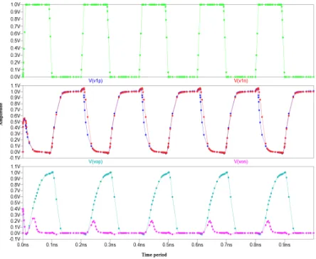
The architecture consists of dynamic preamplifier stage and two latches LAT1 and LAT2 as in Fig 2. The pre-amp operates in the first stage eventually drives the LAT1 and LAT2. Shown in Fig 3 (a) Sharing of the stages will reduce power consumption. Vck0 is the clock input of the dynamic pre-amp which operates at Tck0 clock period whereas the LAT1 and LAT2 operates at 2 x Tck0 as the clock period. The signal pairs are V1p,n and V2p,n are the inputs for which the circuit exhibits the output signal pairs as Vop1/Von1 and Vop2/Von2 respectively.
Fig 3 a. Circuit representation of Switched dynmamic comparator
Fig 3b. Waveform explaining the operation of proposed swiched dynamic comparator
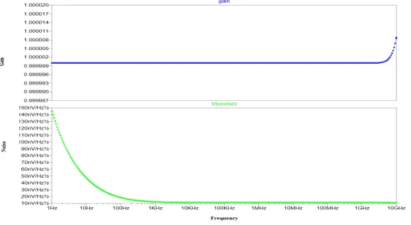
Here the two dynamic comparators in the SDC are exactly the same and we have discussed about one of them as an example. Their operation lies in either “reset” or “regeneration” phase of the time frame. The circuit thus exhibits an extended regeneration time for it to operate at maximum operating frequency which could be inferred from the Fig 3 (b), which is 1.5 times the clock period of Tck0. Thus the clock speed is 3 times that of the conventional dynamic comparators. The simulated signal behaviour of the proposed SDC using a simulation tool is as follows. To dynamically correct the offset error voltage. Tuneable capacitor arrays were added to the nodes V1pn and V2pn depicted in the Fig 4a and 4b.
[image:4.612.166.476.549.709.2]©IJRASET 2015: All Rights are Reserved
238
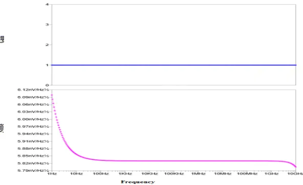
Fig 4b. Signal waveform of SDC with tuneable capacitor array The Noise analysis on the comparator circuitry help us to significantly identify the efficient circuitry,
Fig 5 a. Waveform representing the noise component of the dynamic comparator circuit
[image:5.612.161.457.279.460.2]
Fig 5 c. Waveform representing the noise component of the switched dynamic comparator circuit with tunable capacitor array
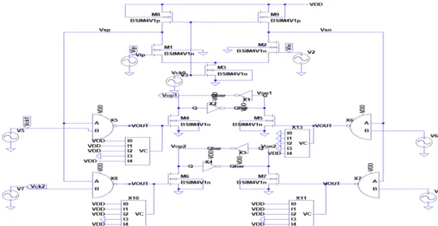
IV.NONINTERLEAVEDFLASHADCARCHITECTURE
[image:6.612.156.455.81.245.2]The block diagram of the ADC architecture shown in Fig 6 is with 15 SDCs quantizes the input signal, followed by encoded and multiplexing circuitry. One reference SDC is used for the background calibration which measured the trip voltage generated by introducing an intentional imbalance in each differential pair [8]. The measured ADC output spectrum obtained with the FFT observed to be 12000 MHz (approximately) for the input signal with full swing at 600 MHz (approximately).
Fig 6. Detailed block diagram of the Full Flash ADC Below are the various essential circuit which are building block of the analog-to-digital converter,
[image:6.612.169.476.540.712.2]©IJRASET 2015: All Rights are Reserved
240
Fig 7 b. Signal waveform of Reference-Switched dynamic comparator
The background calibration circuit shown uses the single reference comparator concept and this scheme is realized by sampling the analog input signal with one R-SDC, the circuit is represented in Fig 7 a, with selectable reference levels from a high-impedance reference ladder, and comparing the results sequentially with each SDC to correct errors in the comparator trip voltages. The R-SDC is a modified version of the SDC [9].
The proper reference voltage VRn should be chosen for the R-SDC, where VRn is the expected trip voltage for SDCn [10]. Since the R-SDC and SDCn sample the same analog input, their outputs should be the same when trip voltages are identical as in Fig 7 b.
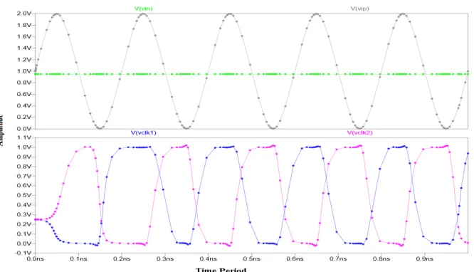
[image:7.612.197.450.371.456.2]Operation of the Flash architecture is governed by the clocking circuit which operates with the differential input producing rail to rail output shown in Fig 8a and 8b.
Fig 8 a. Block diagram of Clock circuitry
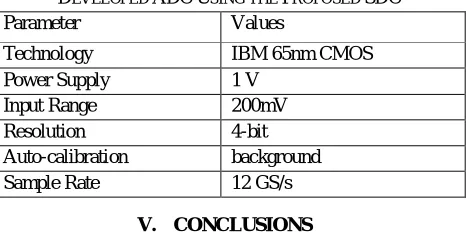
[image:7.612.146.479.504.695.2]Auto-calibration background
Sample Rate 12 GS/s
V. CONCLUSIONS
This paper representing the 12 GS/s ADC using SDC suitable for the SKA receiver chain as it satisfies its requirement of high operating speed, low power consumption. Thus SDC alleviates the phase skew calibration and overcomes the various mismatches experienced with the traditional architectures. Thereby it resolves the speed limitations with the small LSBs in conventional dynamic comparators caused due to the problems with the charging /discharging at the first stage and also due to short regeneration at the second stage of amplification.
REFERENCES
[1] T. Kobayashi, K. Nogami, T. Shirotori and Y. Fujimoto, “A current-controlled latch sense amplifier and a static power-saving input buffer for low-power architecture,” IEEE J. Solid-State Circuits, vol. 28, pp. 523-52, April 1993.
[2] S. Jamal, D. Fu, N.-J. Chang, P. Hurst, and S. Lewis, “A 10 b 120Msample/s time-interleaved analog-to-digital converter with digital background calibration,” IEEE J. Solid-State Circuits, vol. 37, no. 12, pp. 1618–1627, Dec. 2002.
[3] M. El- Chammas and B. Murmann, “General analysis on the impact of phase-skew in time-interleavedADCs,”IEEE Trans. Circuits Syst. I, Fundam. Theory Appl., vol. 56, no. 5, pp. 902–910, May 2009.
[4] M. El-Chammas and B. Murmann, “A 12-GS/s 81-mW 5-bit time-interleaved flash ADC with background timing skew calibration,” in Proc. Symp. VLSI Circuits, Jun. 2010, pp. 157–158.
[5] B. Setterberg, K. Poulton, S. Ray, D. Huber, V. Abramzon, G. Steinbach, et al., “A 14 b 2.5 GS/s 8-way-interleaved pipelined ADC with back-ground calibration and digital dynamic linearity correction,” in IEEE Int. Solid-State Circuits Conf. Dig. Tech. Papers, Feb. 2013, pp. 466–467
[6] M. Miyahara, Y. Asada, P. Daehwa and A. Matsuzawa, “A Low-Noise SelfCalibrating Dynamic Comparator for High-Speed ADCs,” in Proc. A-SSCC, pp. 269-272, Nov. 2008.
[7] H.J. Jeon, Y.B. Kim, “A Low-offset High-speed Double-tail Dual-rail Dynamic Latched Comparator,” ACM GLSVLSI’10(Great Lakes Symposium on VLSI), May 16-18, 2010.
[8] Jun He, Sanyi Zhan, Degang Chen, and R.L. Geiger, “Analyses of Static and Dynamic Random Offset Voltages in Dynamic Comparators,” IEEE Trans. Circuits Syst. I: Reg. Papers, vol. 56, pp. 911-919, May 2009.
[9] Nikoozadeh and B. Murmann, “An Analysis of Latch Comparator Offset Due to Load Capacitor Mismatch,” IEEE Trans. Circuits Syst. II: Exp. Briefs, vol. 53, no. 12, pp. 1398-1402, Dec. 2006.
[image:8.612.191.424.116.232.2]