Design of A Moving Message Dot-Matrix Display
Using At89c52 Microcontroller and Decoders
Engr. Dr. Okwu P I, Ogungberu Oluwaseyi, Engr Okolo Chidiebere C , Engr Okeke Obinna, Engr. Okoye Ngozi B1
1
Electronics Development Institute, Awka, Anambra State, Nigeria
Abstract: The technique and design of a moving message display DOT-Matrix, used in displaying information to the general public electronically was discussed in this article. In this design a highly efficient microcontroller was used. During the design process involves ATMEL 89C52, 3 to 8-line and 4 to 16-line decoders including a three-state buffer/latch were used as the main hardware component while MIDE was used as software elements.
Keywords LEDs, AT89c52 Microcontroller, 74LS138 and 74HCT154 Decoders, 74LS244 Buffers/latch, Perspex
I. INTRODUCTION
A. This can be introduced with the following
1) Microcontroller: This is a computer-in-chip device that is used in controlling the circuit. Being a computer-in-chip means it has all the features of a simple which enables it to function alone independently.
It has features like central processing unit (CPU), memories in the case of RAM-random access memory, ROM-read only memory, registers, input and Output units and other peripherals. In the course of this project I will be using ATMEL microcontroller called AT89C52. This was chosen because of its good memory management and flexibility in usage.
2) Decoders/DE multiplexers: These devices are used in decoding the output signals coming from the output port of a microcontroller to the screen display.
This is achieved using fewer pins as input to it and generating as many output pins, depending on the number of input pins and type. In this project, I am using three decoders (one-74138 and two-74154).
3) Latch: The latching device used on this project is a 3-state buffer (74244) used to boost/amplifier the current signal coming out from the microcontroller and as well help in providing a screen delay that will enable visibility of the message printed on the screen.
This 7424IC is a 20-pin dual-line package device, that has two independent control section inside, each with input and 4-output, making a total of 8-input pins and 8-output pins. It has two enabling pins which are all active low, and then VCC and ground.
4) Drivers Unit: These are the switching section of the circuit comprising of transistors and resistors configure as inverter, used in driving/selecting each of the screen display columns.
For the course of this project BC557 and 1k one quarter watt resistors are used, because of the output of the decoder 74154 which is active low.
5) Screen: This is the display output interface where the message that is to be display by the microcontroller as instructed by my program code that will be displayed in real time.
The screen comprises of two-hundred and twenty-four LEDs (light-emitting diodes) arranged in rows and columns.
6) Power Supply Unit: This section provides power source in the form of DC-current and DC-voltage.
This is made possible by the use of step-down transformer, rectifier diode, filter capacitor, voltage regulator and indicator light with current limiting resistor attached to it.
Technology (IJRASET)
Figure: BLOCK DIAGRAM OF A MOVING MESSAGE DISPLAY
II. METHODOLOGY
A. Component Description
1) AT89C52: This is an ATMEL version of an bit microcontroller comprising of four input/output port, with each port having 8-pins on it. Port one started from the very first pin of the microcontroller i.e. P1.0 to P1.7. Pin 9 is the reset pin of the
microcontroller. Pin 10 to Pin 17 is the port 3 denoted by P3.0 to P3.7. Pin 18 and P19 are the clocking signals of the microcontroller. P20 is the negative supply of the microcontroller called Ground. Pin 21 to Pin 28 is the port 2 denoted by P2.0 to P2.7. Pin 29 is the program store enable denoted by PSEN which is an active low pin. Pin 30 is the Enable pin of the microcontroller denoted as EA. Pin 31 is the address latch enable denoted by ALE. Pin 32 to pin 39 is the port 0, denoted by P0.0 to P0.7. And finally Pin 40 is the positive supply of the microcontroller called VCC. For the purpose of this project, I made use of port 1 as output port to the latch unit (74LS244) and port 2 as the output port to the decoders (74LS138 & 74HCT154).
2) 74LS244: This is a three-state/buffer IC used in latching the screen, in this case the rows of the dot matrix. This component has 20 pins, of which 8 pins are the input pins, while another 8 pins is the output pins and its output and input pins are not linearly positioned. Pin 1 and Pin 19 are the enabling pins and both are active low, meaning it has to be given a low or 0(ground) to activate the IC. Pins(2,4,6,8,11,13,15 & 17) are the input pins of the IC, while Pins(3,5,7,9,12,14,16 & 18) are the output pins of the IC. Pins 10 and 20 are the ground and VCC respectively. The port 1 of the microcontroller are received through input pins of this component and after logical manipulation has been performed on it by the gates, then sent out through the output pins of the IC, to drive each row of the dot matrix.
For the purpose of this project, I made use of seven input and output pins of the IC.
SCREEN
MICRO
CONTROLLER
UNIT
DRIVER/SW
ITCHING
UNIT
DECODER
UNIT
LATCH
UNIT
master decoder in this design to select the other two decoders interface to it. This decoder comprises of 16 pins, out of which three are the input pins(1, 2 & 3), another three are the enabling pins(4,5 & 6; where 4 & 5 are active low and 6 is active high) and another 8-pins are the output pins(7,9,10,11,12,13,14 & 15). While pin 8 and pin 16 are the ground and VCC respectively. For the purpose of this project enable pins of decoder 74154 are connected to the output pin 14 & 15 of the 74138.
4) 74HCT154: This is a 4-to 16-line decoder/DE multiplexer having a total of 24 pins in all, configured to be slave to the 74138 in this design. This decoder has four input pins(20,21,22 & 23) and sixteen output pins(1,2,3,4,5,6,7,8,9,10,11,13,14,15,16 & 17). These output pins are active low. Pins 18 & 19 are the enable pins of the decoder, denoted as E1 & E2 and both are active low. These two enables are bridged or shorted together and a single output sent out from it to the out of the 74138 decoder for enabling/selecting. Pins 12 & 16 are the ground and VCC respectively. For the purpose of this project the 74154 was used because of its fewer input to many output feature. The outputs of this decoder are connected to the switching transistor BC557 through a base biasing resistors.
5) BC557 & 1K Resistor: these two components are what make-up switching part/driver section of the circuit. The BC557 is a PNP type low signal bi-polar transistor together with its base biasing resistor 1-kilo ohms which is rated ¼ watt. ¼ watt was chosen because of its small size, thereby occupying little space and also its low power dissipation property compared to bigger sizes. The BC557 is a center based type of bi-polar transistor. The output of the decoder passes through a resistor to their bases, while the emitter terminal was connected to positive signal (i.e. VCC) permanently. Then this flows out through the collector terminal to the various columns of the screen, as soon as the base has been biased. BC557 was used for the purpose of this project because the outputs of the decoders that will biases its base are active low (i.e. negative signal). So to achieve inversion, I needed a negative based PNP type bi-polar transistor.
6) Board/Screen and LED: For the purpose of this project I chose 5x7 character design model and because I wanted it to be displaying 6-characters at once, I went for 32x7 (i.e. 32-columns and 7-rows). Here I made use of ceiling board sheet instead of perspex because of the number of advantages it offers as against perspex, advantages like;
a) Easiness to drill and work on,
b) Low cost as compare to perspex.
But though it has its own disadvantages like;
a) Tear due to rough handling
b) Consumes more paint
7) Design and Construction
- Marking out and cutting of the board:
Since I am designing 32x7, then means that the number of holes/LEDs to be perforated/inserted is; 32 multiply by 7, which is 224 holes.
The size of my board will be: 28 inches by 7 inches LED size: 5mm
The hole spacing at columns and rows is 20mm.
I used metal rule and pencil to do my markings on the board.
- Hole drilling: I used a hand electric drilling machine with a drilling bit size of 5mm as regards the size of the LED that I was using, to bore a hole on the board through those markings on the board.
- Spray Paint: for this project I made use of ABRO spray paint black, because of its fast drying quality and smoothness.
- Insertion of LEDs and Soldering: In this section the LEDs was inserted in a definite pattern of arrangement. For the course of this project, I adopted common cathode arrangement of the LEDs. Whereby all the cathode on a row are joined together, while the anode are connected together along the column. After which soldering took place.
B. Power Supply Unit
Components that makes up a simple power supply unit are;
1) Step-down Transformer
2) Rectifying Diode
Technology (IJRASET)
4) Voltage Regulator
5) Indicator Light
Step-down Transformer: A step-down transformer is used in stepping down the input voltage of an AC supply to a lower output voltage still AC. For the purpose of this project, I chose 12x1: 220VAC – 12VAC / 500mA Transformer.
Why did I chose 12x1 instead of 12x2?
Since from our circuit schematic diagram, there is no section that requires a negative voltage, because using 12x2 type, it simply mean that the transformer has two output supply wire and a center tapped which is the ground. So in other to reduce cost and complexity of the circuit, I made use of 12x1 which does not have center tapped terminal.
Why should it be 12VAC/500mA output supply?
The need for 12VAC/500mA output arises from the fact that in our circuit schematic, all the components that I used in the circuit makes use of 5VDC supply. And this is made possible by a 5V regulator (7805), which according to its datasheet requires a minimum voltage of 7V coming in to it as input before it will regulate it to 5V.
Rectifying Diode: this is a component that is used in converting the AC voltage from the output of a transformer to a DC voltage. For the purpose of the project, I chose 1N4007 connected in a bridge topology. The reason is that, the output current rating of the transformer is 500mA and according to 1N4007 datasheet, it can be able to source up to 1000mA and a maximum voltage of 600V. Flter Capacitor: This is where filtration process takes place, filtering off trace of AC ripples from the rectified DC voltage. The value of the capacitance and voltage of the capacitor is much more dependent to the output supply from the transformer.
6) How to calculate the capacitance of the filter capacitor
Capacitance C, = Quantity of current Q
Ripple voltage Vr
Where Q= IT but recall that T= 1/F Therefore Q= I/F
Where I is the current rating of the transformer F is the frequency of the transformer Since our Transformer rating is; I = 500mA F = 50Hz Vrms = 12VAC
Peak voltage Vp = Vrms √2 = 12√2 = 16.971VMAX
The biasing voltage of a silcon diode is 0.7V, therefore the two diodes is = 2 x 0.7V
= 1.4V Then,
Vr = 16.971 – 1.4 – 7V = 8.571V
Since the diode setup is in a modified full wave rectification, the frequency is doubled. I.e. F = 2 x 50Hz
= 100Hz Therefore, C =
= ×
× .
= 5.833625 x 10⁻⁴ F = 583.36 µF
Operating voltage = Vr x 1.5
= 8.571 x 1.5 = 12.8565V
Therefore any capacitor from 16V rating and above is good, to avoid the capacitor blowing up due to excessive voltage. Voltage Regulator: This component keeps the output voltage from the capacitor to a constant value as long as its minimum operating voltage as required by its datasheet. In the case of this project, I made use of LM7805, which by its datasheet requires a minimum input voltage of 7VDC to be able to give out 5V regulated voltage output.
Indicator light: indicator light is incorporated in the power supply section, to indicate when the circuit is active. The indicator light is an LED bulb connected in series with a 1KiloOhm current limiting resistor, to protect it against excessive current that will damage it.
7) Project Implementation, Testing and Results
This is where the workability of the circuit, ideas and laydown technicalities are being enforced. I achieved this using
a) MIDE software: for development and compliering of the program code in assembly language, which configures the internal circuitry of the microcontroller used.
b) Protues professionals: This is a virtual laboratory circuit board used to draw and simulate the circuit. This was done to determine its functionality, for easy implementation on a vero board or PCB.
c) Eagle CADsoft: this software was used in drawing and designing of the printed circuit board (PCB) for easy implantation of the circuit. And because of its qualities, it is professional to implement circuit with it.
Flow chart of the code
IF NO IF NO
IF YES
START
GENERATE CODES FOR CHARACTERS
CHECK UP CHARACTER ON
THE TABLE
IS CHARACTER
CALLED? INITIALIZATION
Technology (IJRASET)
IF NO
[image:7.612.95.392.67.361.2]IF YES
Figure 1.2 Flow chart of the program code
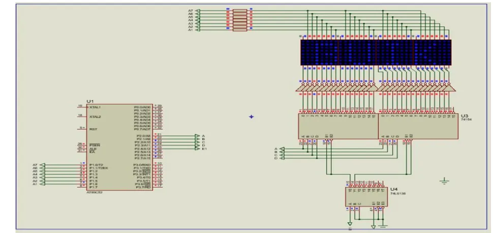
8) The Proteus Simulation: Blow is the circuit schematic diagram of the moving message display, simulated using proteus professional.
Figure: Result of the proteus simulation of a dot-MAT moving message display.
REFERENCES
[1] Wu Gang, Application of AT89C52 microcontroller in the hospital care[J] Electronics Component and Device APPLICATIONS, 2008. [2] Zhou Mingde, Principle and Application of Micro Computer System [M], Beijing; Tsinghua University Pree, 2007.
[3] Yen Shi, Digital Electronics Technology [M], Beijing; Higher Education Press, 2015
LOAD CHARACTER IN MEMORY LOCATION
SHIFT CHARACTER FROM ONE MEMORY LOCATION
TO ANOTHER
CHECK IF TARGET MEMORY LOCATION HAVE BEEN REACHED
[image:7.612.57.542.398.627.2]