International Journal of Emerging Technology and Advanced Engineering
Website: www.ijetae.com (ISSN 2250-2459, ISO 9001:2008 Certified Journal, Volume 5, Issue 1, January 2015)
236
Efficient Routing Implementation of Programmable Network on
Chip on FPGA using Circuit Switching Approach
Parag Parandkar
1, Purnima Khandelwal
2, Geetesh Kwatra
3,
Sumant Katiyal
41
Research Scholar, Devi Ahilya University, Indore (M. P.), India
2M. Tech. Scholar Oriental University, Indore (M.P.), India
3Assistant Professor, Chamelidevi School of Engineering, Indore (M.P.),India 4
Professor, School of Electronics, Devi Ahilya University, Indore (M. P.), India
Abstract—More and more complex and larger system on
chips are getting developed as a result of increase in chip density following Moore’s law. Advanced SoCs have in their shelf significantly noticeable communication mechanisms. NoC has solved the scalability problems to a larger extent compared to bus based interconnect. NoC has been providing a back bone infrastructure for System-on-chips since long. Among the available communication matrices NoC has helped tremendously in the communication performance enhancement. NoC research majorly involves work on packet switching, though at the same time circuit switching assures high communication rates and predictable communication latencies. The current research is targeted towards implementation of NoC architecture for FPGA based designs using circuit switching approach. Proposed implementation is termed as enhancement of light weight circuit switched architecture. The programmable NoC architecture is being implemented using VHDL and synthesized on the Virtex-5 XC5VLX20T package FF323 device at 139 MHz. It provides sufficient customization on the number of ports, nodes and amount of data. Performance improvement over the existing implementations has been validated by the experimental synthesized results.
Keywords— Circuit Switching, FPGA, Network Topology,
Packet Switching, Programmable NoC.
I. INTRODUCTION
The implementation of very large systems on a single chip is termed as System on chip (SoC). These architectures generally consist of combination of CPUs, memories and custom hardware models. SoCs could also be put into practice on Programmable Logic Devices (PLDs), e.g. Field Programmable Gate Arrays (FPGA) or Complex Programmable Logic Device (CPLD). The emergence of programmable SoCs have made significant contribution in on chip system world because of two major reasons mentioned under: i) At first bus based communication creates scalability issues with increasing system complexity and could prove to be an important bottleneck, thus giving rise of the adoption of Network on chip architecture.
NoCs have successfully addressed the problem of SoC scalability. The concept of programmability among NoC has been taken into consideration by architecting them for the varied applications taking different shapes for different applications at various times. ii) Second issue deals with design and verification, which again becomes very important to deal with at the level of higher complexities. FPGA based communication could become a very viable solution in this case, as design and verification could be repeated n number of times for any design idea within FPGA.
A computing architecture for FPGAs has greatly simplified application development. It should abstract away the differences between FPGA devices, while supporting communications with external devices at full interface speed, consuming as few resources as possible, and allowing the application to determine how data should be handled.
FPGAs have since long been shown to be effective and efficient for performing a variety of computations [2-6]. But at the same time the high non recurring engineering costs and long time to market for ASICs, clearly indicates more better use of FPGAs for designing different hardware applications [2].
International Journal of Emerging Technology and Advanced Engineering
Website: www.ijetae.com (ISSN 2250-2459, ISO 9001:2008 Certified Journal, Volume 5, Issue 1, January 2015)
237
N
W E
S C
W
IP 0
(0,0)
1
(0,1)
2
(0,2)
3
(1,0)
4
(1,1)
5
(1,2)
6
(2,0)
7
(2,1)
8
(2,2) This proposal introduces a new modified architecture for
FPGA computing that will provide a standard for FPGA communication, and ease the burden of implementing application coordination and managing communication for both on and off chip. Circuit switched NoC based architecture was proposed in [9], so as to facilitate the process of porting a traditional hardware implementation to NoC based implementation.
Programmable NoC is very flexible and light weight architecture for FPGA based system. It is a modular design that utilizes standard interfaces and Intellectual Property cores [10].
Best Scalability and higher communication bandwidth are the key advantages and features of programmable NoC. The architecture described in [9] was implemented in JHDL [11], which is of remote use as far as Hardware description languages are concerned. [1] used the PNoC implementation in Verilog HDL using the choice of Xilinx Virtex Pro FPGA that resulted in a particular clock frequency (127 MHz) after synthesis.
In the proposed work using another HDL, that is, VHSIC Hardware Description Language (VHDL), the implementation of Programmable NoC architecture is being carried out. The choice of FPGA has also been revised to more resourceful and popularly available Xilinx Virtex 5. The result of the architecture is consistent and slightly better as compared to the one proposed in [1] and [9].
The rest of the paper is organized as follows: Section II provide basic introduction about NoC architectures. Related work is shown in Section III. Section IV described architectural view of VHDL implementation of programmable NoC architecture. Section V outlines results. Section VI concludes the paper.
II. NOCARCHITECTURAL BASICS
With the rise in system complexity and level of integration tend towards ULSI to GSI and at the verge of introducing SoCs, the bus based communication systems have not proved to be effective in terms of scalability, and design verification. Furthermore, day to day electronics markets encompassing consumer electronics markets have made the requirement for higher computational speeds and lower power consumption to be necessarily incorporated. The NoC architectures bridged this technology gap and provide the well needed possible solutions to these problems.
The basic NoC architecture is as shown in Fig. I. It consists of processing elements, connection topology, routing technique, switches and programming model.
There are varieties of topologies possible in NoCs. Some of these are torus, octagon, mesh, ring and irregular topologies [12, 13]. The most conventional and most popular topology utilized in the most of the research proposals uses mesh topology, as it provides better routing and low latency [14].
NoC by its architecture composed of interconnection of IP cores connected together by the help of routers. These IP cores could have been very well act as processors while designing MPSoCs. NoC provides long list of benefits for design space exploration and performance analysis by using IP macro cells in plug and play fashion. Scalability and reusability are the key benefits of NoC based implementations that also helps in reducing time to market and development costs. A common hardware design could not be so easily translated into NoC based design as design needs to be divided in different processing units and then on this platform the communication mechanism could be very well defined.
FIG.I BASIC NETWORK ON CHIP ARCHITECTURE
There are two types of switching possible in NoCs: Packet switching and Circuit Switching. Packet switched networks uses three switching techniques: Virtual cut through switching, Store and forward and Wormhole. Virtual cut through switching divides packets into flits and then into phits. This switching technique is not so widely popular and used to a lesser extent. In store and forward switching, packet is routed only if the receiving buffer has enough space to accommodate this packet [17]. This switching technique is used in computer networks and is not much used within the chip. In the wormhole switching [18], packet has been routed first by header and then the rest. So the latency is experienced only by header and the remaining packet follows the header. This switching technique is most popular in the design of NoC circuits.
International Journal of Emerging Technology and Advanced Engineering
Website: www.ijetae.com (ISSN 2250-2459, ISO 9001:2008 Certified Journal, Volume 5, Issue 1, January 2015)
238 Though it is a very scalable architecture still this seems to be unsuitable for some heavy dataflow applications, being lagging in performance. Marescaux et al. [27] used FPGAs specifically. It is a 2D torus architecture that performs packet switching using wormhole routing. It uses partial FPGA reconfiguration to support run-time module replacement.
Circuit switching techniques reserve the path before the transmission of data while packet switched networks uses buffers to store data. It establishes dedicated connection path (a virtual circuit) between two nodes, before actual communication. After the establishment of the virtual path, data can be transferred with very low overhead between the modules, till the time data transfer ends up; virtual circuit gets closed. These networks does not need overhead of packetisation, processing of packet header or buffering of packets. This flexibility of circuit switched approach makes it feasible for its use in regular topologies like that of mesh and ring and irregular topologies as well. Peak bandwidth could also be attained without much of the efforts. However two important shortcomings of circuit switching are mentioned as under: i) Setup latency, which is the time required to build up a virtual circuit. This latency in incurred compulsorily in circuit switching before start of communication between nodes. In the proposed method, by using simple communication protocols, modified approach this circuit establishment latency is minimized. ii) Spending idle time on communication links, which is the time when the connection has been established, but there are no data transfers. This is also not a major cause of concern in the proposed modified approach as very short time interval is used for opening and closing of connection. Some references for circuit switching architectures in NoC design includes Lin and Co-workers [28,29] that advocates circuit switching over packet switching. Lin et al. [28] proposed the time division multiplexed central switched network (crossbar) shared by all communication nodes. SoCBUS [29] uses circuit switched NoC organized as fixed 2D mesh, involves routing switch for every computing node. Both [28, 29] performed detailed simulations of circuit switched NoCs and through the results of throughput advocated the advantages of circuit switched networks over packet switched networks.
Proposed work involves detailed modified implementation of a circuit switched NoC on FPGA. Circuit switched architecture is preferred over packet switched architecture on account of maintaining guaranteed throughput between nodes through virtual circuit.
Packet switching could incur variations in communication latencies. The topology flexibility of the system also places it over other regular mesh and other crossbar architectures.
Goals of the proposed design are mentioned as under: To design a flexible approach, so that: i) It is applicable to wide range of system requirements. ii) It offers allowable network topologies and communication data path widths. iii) It establishes light weight network which uses minimal FPGA resources.
III. RELATED WORK
The NoC is basically used to provide high performance clubbed with low power consumption for System-on-chip architectures. They have been implemented in different configurations and provide lots of capabilities. Below mentioned is a summary of some of the popular NoC architectures.
Xpipes architecture [19] is based on heterogeneous model, unlike NoCs, which are primarily based on a homogeneous model. Due to its heterogeneous nature, it requires huge efforts in its implementation phase.
Agarwal and Shankar exploited the high performance computing capability of NoCs and they have proposed a layered architecture for NoC based systems [7]. Their architecture consists of different domains, including protocol on a NoC environment, algorithms, applications, and RTOS. Their proposed design was parameterized. This implementation uses Mission Level Designer (MLD), which is not a commonly used environment. This environment is not the best suitable one for the proposed NoC architecture development [31]. Arteris [20] is one of the commercially available NoC implementations. However, Arteris implementation realistically involves very high licensing fee pertaining to its commercial nature. The virtual channel (VC) is an important constituent of NoC as it provides virtual paths for the flow of data in the form of flits, thus avoids deadlocks to a great extent. In [21], Bjerregaard and Sparsø proposed a new implementation of a virtual channel router using asynchronous techniques for circuit implementation.
International Journal of Emerging Technology and Advanced Engineering
Website: www.ijetae.com (ISSN 2250-2459, ISO 9001:2008 Certified Journal, Volume 5, Issue 1, January 2015)
239 Some Ad-hoc switching techniques were developed by the combination of various switching techniques [23, 24]. Technique of using Communication Dependency Graph (CDG) for inter-process communications is done by Siebenborn et al. [25]. Use of Communication dependency graph involves load balancing, placement, and fanout routing, which is not easy to implement. The topologies torus, mesh, and cube networks are compared by Neeb et al.[26].
All the aforementioned NoC architectures are highly specific to a particular application and also complex ones. They are not generic ones which could be utilized flexibly for more applications by concept of reuse. In the proposed modified implementation we tend to implement flexible and light weight NoC architecture. We have implemented an improved version of a light weight circuit switched NoC for FPGA systems by [1]. It is being designed keeping in view three basic parameters: Flexibility, use of standard network interfaces and simplified network protocols. Implementation includes a light weight network that utilizes fewer FPGA resources and could be programmed on state-of-the-art FPGAs [30]. The earlier design implementation was done using Verilog HDL [1]. The proposed design is being improvised and programmed in VHDL. Also at the same time it incorporates better resource utilization in terms of selecting Virtex-5 FGPA thus incorporating better results in terms of clock frequency.
IV. PROGRAMMABLE NOC:CIRCUIT SWITCHED FPGA BASED NOCARCHITECTURE
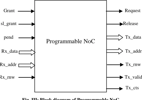
[image:4.612.325.541.120.240.2]Programmable NoC is a circuit switched architecture that simplifies the system design by providing flexible networking approach. It is possible to design various network architectures each with its own choice of system routing. The nodes can be dynamically inserted and removed, provided the FPGA supports it. It consists of sub nets, which are in turn connected to router and a bunch of network nodes as shown in Fig II ([1] and [9]]. This type of architecture was chosen on account of its ability to place modules that communicate very frequently in the same subnet, thus allowing more effective system communication. A simple handshaking mechanism is used to establish dedicated connections between nodes, to exchange data and to remove connections.
Fig. II : PROGRAMMABLE NETWORK ON CHIP TOPOLOGY
The circuit switching between the nodes is performed by the router. Each node is connected to the router by a router-port interface. A simple handshaking mechanism is used to establish a dedicated connection for the data exchange and connection removal.
For the connection to be established, master node (A) sends the request signal along with the address of the target node (B) to the router. The second router sends the grant signal to the first router that port B is available. Thus the connection is established through this simple mechanism.
Dedicated connection between nodes is supported by using light weight handshaking mechanism, so as to be used for removing connections.
The circuit switched architecture uses following signals:
Fig. III: Block diagram of Programmable NoC
The single bit control signals are used for router table updates, requests to create and destroy virtual circuits and read/write requests. Along with this each module has a set of receive and transmit signals having address and data liens. Transmit address lines serve multiple purpose. In the virtual circuit creation, they specify the ID (or address) of the module requiring virtual connection.
Node
A 1
3
5
7
2
4
6
8
Router 1
3
5
7
2
4
6
8
Router Node
B
Request
Release
Tx_data
Tx_addr
Tx_rnw
Tx_valid Grant
sl_grant
pend
Rx_data
Rx_addr
Rx_rnw
Programmable NoC
[image:4.612.328.561.422.586.2]International Journal of Emerging Technology and Advanced Engineering
Website: www.ijetae.com (ISSN 2250-2459, ISO 9001:2008 Certified Journal, Volume 5, Issue 1, January 2015)
240 Read and write transactions begin after the establishment of virtual connection. These transactions specify address in remote module‘s address space to which it refers. cts signals are utilized for flow control mechanism.
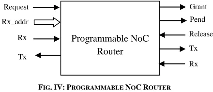
Programmable NoC Router Design:
Programmable NoC consists of following signals as shown in following Fig:
FIG.IV:PROGRAMMABLE NOCROUTER
It contains the blocks of Table arbiter, routing table, Port queue, port arbiter, switch box.
Routing is done via router‘s switch box. The switchbox is configured in such a way that any given Rx line could be connected to any of the available Tx line.
Programmable NoC connects to the CPU like any other module. The interfacing circuits like that of FIFOs and FSM are connected with the router. Programmable NoC has router as its main component. It includes routing table, queue and switch box. Buffer is parameterizable in the design as needed so. Buffers accommodate data in two conditions: if nodes and routers are running at different clock rates and when there is difference between the transmitting and receiving rates.
Implementation in VHDL consists of Router entity as main entity which acts as top level module. It consists of three sub modules as shown in Fig. II. The buffer module is used to do two tasks: FIFO control and memory. FIFO control monitors different signals for buffer like buffer empty, buffer full, memory pointer etc. Memory is used to store the data that comes into the buffer.
MUX entity is used to select data lines on the basis of select lines. The select lines of MUX keep up a correspondence with the address lines of the memory.
The router module which happens to be the main module is the switching module. It directs data to a path, which is decided on the basis of address and data coming from the buffer and MUX. The router entity (Top level entity) connects all other lower level entities.
[image:5.612.60.280.223.318.2]V. EXPERIMENTAL RESULTS
Table 1below shows the comparison of implementations from [1] and the proposed NoC implementation. This set up was designed to exhibit maximum data transfer ability.
The device, ports and data widths are used as earlier implementations. The results are slightly better instead of using same implementations, not by accord of change of HDL from Verilog to VHDL, but because of the use of state-of-the-art Virtex 5 FPGA having more resourcefulness as compared to earlier one.
TABLE I:
COMPARISON OF DIFFERENT PNOC IMPLEMENTATIONS
S. No.
Specification Uzma Mushtaq et.al
PNoC[1]
Proposed Programmable
NoC
1. Language Verilog HDL VHDL
2. Device Xilinx
Virtex – II Pro FPGA (vcv2p30-7)
Xilinx Virtex-5 XC5VLX20T FPGA FF323
3. Clock Speed (MHz) 126.486 139
4. Ports 8 8
5. Data Width 8 8
6. Area (slices) 1227 1305
VI. CONCLUSION
Flexible light weight circuit switched approach is depicted for FPGA based systems. The work has been shown to be delivering better results in terms of clock frequency improvisation compared to the earlier implementations. The Programmable NoC architecture is implemented using VHDL on the Virtex-5 XC5VLX20T package FF323 device at 139 MHz. It provides sufficient customization on the number of ports, nodes and amount of data. Performance improvement over the existing implementations has been validated by the experimental synthesis results. This encourages current design to be further modified and enhanced using higher level Hardware languages working on system level, like that of SystemC and System Verilog.
REFERENCES
[1] Mushtaq U., Hasan, O. ; Awwad, F.; ―PNOC: Implementation on Verilog for FPGA‖, 9th IEEE International Conference on Innovations in Information Technology (IIT), 17-19 March, 2013, Abudhabi, pp. 148-151 10.1109/Innovations.2013.6544409.
[2] Shuai Che, Jie Li, Jeremy W. Sheaffer, Kevin Skadron, and John Lach. ―Accelerating Compute-Intensive Applications with GPUs and FPGAs‖ in Proceedings of the 2008 Symposium on Application Specific Processors, SASP ‘08, pages 101–107. IEEE Computer Society, 2008.
[3] Eric S. Chung, Peter A. Milder, James C. Hoe, and Ken Mai. ―Single- Chip Heterogeneous Computing : Does the Future Include Custom Logic , FPGAs , and GPGPUs?‖, International Symposium on Microarchitecture (MICRO-43), Atlanta, GA, 2010, pages 225– 236, 2010.
Request
Rx_addr
Rx
Grant
Pend
Release
Tx Tx
Rx
[image:5.612.320.568.230.380.2]International Journal of Emerging Technology and Advanced Engineering
Website: www.ijetae.com (ISSN 2250-2459, ISO 9001:2008 Certified Journal, Volume 5, Issue 1, January 2015)
241
[4] David Barrie Thomas, Lee Howes, and Wayne Luk. ―A Comparison of CPUs, GPUs, FPGAs, and Massively Parallel Processor Arrays or Random Number Generation‖ in Proceedings of the ACM/SIGDA International Symposium on Field Programmable Gate Arrays, FPGA ‘09, pages 63–72. ACM, 2009.
[5] Jeremy Fowers, Greg Brown, Patrick Cooke, and Greg Stitt. ―A Performance and Energy Comparison of FPGAs, GPUs, and Multicores for Sliding-Window Applications‖ in Proceedings of the ACM/SIGDA International Symposium on Field Programmable Gate Arrays, FPGA ‘12, pages 47–56. ACM, 2012.
[6] Altera. Altera Annual Report (2012 Form 10-K). http://www:sec:gov/Archives/edgar/data/768251/000076825113 000008/altera10k12312012:htm.
[7] A.Agarwal and R. Shankar, ―A layered architecture for NOC design methodology‖, IASTED International Conference on Parallel and Distributed Computing and Systems, pp. 659-666, 2005.
[8] L. Benini and G. De Micheli, ― Networks on Chip: a New SoC Paradigm‖, IEEE Computer, volume1, pp. 70– 78, 2002.
[9] C.Hilton and B. Nelson, ―PNoC: A flexible circuit switched NoC for FPGA-based systems,‖ IEE proceedings computers and digital techniques, volume 153 Issue 3, 2006.
[10] E. Salminen, V. Lahtinen, K. Kuusilinna, and T. Hamalainen, ―Overview of bus-based system-on-chip interconnections,‖ in Proceedings of the IEEE International Symposium on Circuits and Systems.ISCAS 02, , pp. 372–375 vol.2, 2002.
[11] Hutchings, B., Bellows, P., Hawkins, J., Hemmert, S., Nelson, B., and Rytting, M., ―A CAD suite for high performance FPGA design‖, in Pocek, K.L., and Arnold, J.M. (Eds.). Proc. IEEE Workshop on FPGAs for Custom Computing Machines, Napa, CA, USA, pp. 175- 184, 1999, (IEEE Computer Society).
[12] J. Dally and B. Towles Principles and Practices of Interconnection Networks, Morgan Kaufmann, 2004.
[13] A. Ivanov, C. Grecu, M. Jones, P. Pratim Pande, and R. Saleh, P. Pratim Pande, C. Grecu, M. Jones, A. Ivanov, and R. Saleh, ―Performance evaluation and design tradeoffs for network-on-chip interconnect architectures‖,IEEE Transactions on Computers, volume54, no. 8, pp. 1025-1040, 2005.
[14] Hosseinabady, M.; Kakoee, M.R.; Mathew, J.; Pradhan, D.K.; , "Low Latency and Energy Efficient Scalable Architecture for Massive NoCs Using Generalized de Bruijn Graph," IEEE Transactions on Very Large Scale Integration (VLSI) Systems, vol.19, no.8, pp.1469- 1480, Aug. 2011.
[15] J. W. Dally and B. Towles, ―Route packets, not wires:‖On-Chip interconnection networks‖, Proc. IEEE International Conference on Design and Automation, pp. 684-689,2001.
[16] P. T. Wolkotte, G. J. M. Smit, G. K. Rauwerda, and L. T. Smit, ―An energy-efficient reconfigurable circuits switched network-on-chip‖, Proc. 19th IEEE International Conference on Parallel and Distributed Processing Symposium, pp. 155-163, 2005.
[17] M. Millberg, E. Nilsson, R. Thid, S. Kumar, and A. Jantsch. ―The Nostrum backbone - A communication protocol stack for networks on chip‖, Proc. IEEE International Conference on VLSI Design, pp. 693, 2004.
[18] K. M. Al-Tawil, M. Abd-El-Barr, and F. Ashraf, ―A survey and comparison of wormhole routing techniques in mesh networks‖, IEEE Network, volume11, pp. 38– 45, 1997.
[19] D. Bertozzi and L. Benini, ―Xpipes: A network-on chip architecture for gigascale systems-on-chip‖, IEEE Circuits and Systems Magazine, volume4, Issue 2, pp. 18-31, 2004.
[20] ARTERIS. A comparison of network-on-chip and buses. Whitepaper, 2005. http://www.arteris.com/nocwhitepaper.pdf.
[21] T. Bjerregaard and J. Sparsø, ―A router architecture for connection- oriented service guarantees in the MANGO clockless Network-on- Chip‖, Proc. Of IEEE on Design Automation and Test, volume2, pp. 1226-1231, 2005.
[22] S. Kumar, A. Jantsch, J-P. Soininen, M. Forsell, M. Millberg, J. Oberg, K. Tiensyrja, and A. Hemani, ―A network on chip rchitecture and design methodology‖, IEEE Computer, pp. 117-124, 2002.
[23] E. Rijpkema, K. Goossens, A. Radulescu, J. Dielissen, J. van Meerbergen, P. Wielage, and E. Waterlander, ―Trade-offs in the design of a router with both guaranteed and best-effort services for networks on chip‖, IEE Proc. on Computers and Digital Techniques, volume150, Issue 5, pp. 294-302, 2003.
[24] K. Goossens, J. Dielissen, and A. Radulescu, ―A Ethereal network on chip: Concepts, architectures, and implementations‖, IEEE Design & Test of Computers, volume22, Issue 5, pp. 414-421,2005. [25] A. Siebenborn, O. Bringmann, and W. Rosenstiel, ―Communication
analysis for network-on-chip design‖, Proc. IEEE International conference on Parallel Computing in Electrical Engineering, pp. 315-320, 2004.
[26] C. Neeb, M. Thul, and N. Andwehn, ―Network on-chip centric approach to interleaving in high throughput channel decoders‖, Proc. IEEE International Symposium on Circuits and Systems, pp. 1766– 1769, 2005.
[27] Marescaux, T., Bartic, A., Verkest, D., Vernalde, S., and Lauwereins, S.: ‗Interconnection networks enable fine-grain dynamic multi-tasking on FPGAs‘. Proc. 12th Int. Conf. on Field- Programmable Logic and Applications, FPL ‘02, September 2002, pp. 795–805.
[28] Liu, J., Zheng, L.-R., and Tenhunen, H.: ‗A circuit-switched network architecture for network-on-chip‘. Proc. Int. Symp. On System-on- Chip, September 2004, pp. 55–58.
[29] Wiklund, D., and Liu, D.: ‗SoCBUS: switched network on chip for hard real time embedded systems‘. Proc. Int. Parallel and Distributed Processing Symp., April 2003.
[30] http://save.seecs.nust.edu.pk/pubs/INNOV13.pdf.