Printed Leaf Shaped Monopole Antenna
R.Seetharaman , E.Gowtham Raj
P.Geethanjali, S.Hariram.
Department of ECE College of Engineering – Guindy, Anna University, Chennai -600025 India.
M.Kannan.
Department of Electronics Engineering, Madras Institute of Technology- Chromepet
Anna University, Chennai-600044 India
ABSTRACT
This paper presents a printed leaf shaped antenna with a rectangular ground plane which belongs to the class of printed monopole antenna and is small (16 cm2), compact, conformal and provides an ultra wide band performance giving very good omnidirectional radiation pattern similar to monopole antenna. It has an impedance bandwidth of around 10.25 GHz (return loss< 10 dB) ranging from 3.0251 GHz - 13.2848 GHz and a constant group delay over this range.
General Terms
Printed monopole antenna, UWB antenna.
Keywords
Group delay, 3D radiation pattern, gain.
1.
INTRODUCTION
Ultra Wide Band (UWB) is an emerging wireless technology for commercial high-data-rate, short range communications, radar systems, and measurement. Since 1970’s, UWB radio technology has been investigated thoroughly and developed for wireless communications. The Federal Communication Commission (FCC) regulated the emission limits of -41.3dBm/Hz for an allocated spectrum ranging from 3.1GHz to 10.6 GHz. UWB devices are typically used to transmit and /or receive signals with very short pulses, which may be modulated in UWB communication systems.
The extremely short pulses in time domain usually occupy ultra wide band in the frequency domain. Owing to potential interference with the existing narrowband systems, the FCC regulated the emission limits, for instance, the effective isotropic radiated power (EIRP) levels of -41.3dBm/MHz for the allocated 7.5GHz bandwidth (3.1-10.6 GHZ) for the unlicensed use of commercial UWB communication systems. The commercial UWB device defined by the FCC includes imaging systems, vehicular radar systems, communications and measurement systems. As technology advances smaller devices that operate over the UWB range are required. These antennas have to be small, conformal, compact providing ultra wideband performance with omnidirectional radiation pattern with a linear phase [24].
Linear phase is required for optimal wave reception, which corresponds to nearly constant group delay. This minimizes pulse distortion during transmission. In addition to linear phase, high radiation efficiency is required for UWB applications. Typical antennas sold out commercially achieve efficiencies of 50-60% due to lossy dielectrics. A power loss of 50% is not acceptable for UWB since the receive end architecture must be exceptionally sensitive to receive a UWB
UWB applications. Since the transmit power is so low, power loss due to dielectrics and conductor losses must be minimized.
Monopole antenna which is a modified version of the dipole provides omnidirectional radiation pattern but these are three dimensional antennas and cannot be incorporated into smaller devices [3]. If the thickness of the monopole antenna is reduced to that of a plane the resultant antennas are called planar antennas [1]-[5]. These provide a larger bandwidth than their monopole counterparts but still these are not compact enough to be incorporated into smaller devices. Microstrip patch antennas are compact and conformal but these are inherently narrow band antennas because of their resonant nature [24]. Several techniques have been proposed in literature to enhance the bandwidth of microstrip patch antennas but these would either increase the size of the antenna or the impedance match throughout the UWB range will not be perfect [22],[24].
Printed antennas have the design of patch antennas but envisage characteristics similar to that of a monopole antenna. These are small, conformal and have a wide impedance bandwidth. Many printed antennas have been discussed in literature [6]-[22].
This paper discusses a leaf shaped printed antenna which belongs to a class of printed monopole antennas that meets the above UWB requirements. All the simulations are carried out using Ansoft HFSS software.
2.
STRUCTURE
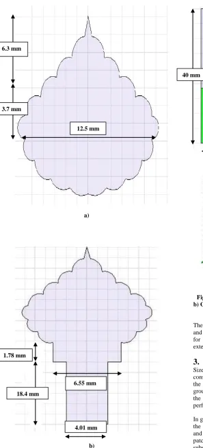
The geometry and coordinate system for the proposed printed monopole antenna fed by a 50 Ω microstrip feed line is shown in Figure 1. It is printed on a Roger RT/ Duroid 5880(tm) substrate with a thickness of 1.6mm, relative permittivity of 2.2 and a dielectric loss tangent of 0.0009.
The width of the microstrip feed line is fixed at 4.01 mm for 50 Ω impedance. A rectangle of cross section 6.55 mm × 1.78 mm is connected between the patch and the 50 Ω feed line for impedance matching (quarter wave transformer). The substrate is of length 40 mm and width 40 mm.
a)
b)
Figure.1 a) Geometry of printed leaf shaped antenna. b)
Geometry of printed leaf shaped antenna with feed lines.
a)
b)
Figure.2 a) Top view of the leaf shaped printed antenna. b) Geometry of Printed leaf shaped antenna with substrate
and ground plane.
The radius of each arc on the edge of the patch is 0.563 mm and length of each arc is 2.124 mm. The above dimensions are for optimum performance of the antenna got as a result of extensive simulations.
3.
DESIGN
Size and shape of the patch, height of the substrate, dielectric constant of the substrate, size and shape of the ground plane, the distance between the bottom edge of the patch and the ground plane are the factors that influence the parameters of the antenna. Optimizing these values for a specific performance is a tedious process.
In general there are no set of rules on selection of the shape of the patch, height of the substrate, shape of the ground plane and dielectric constant of the substrate. The shape of the patch, height of the substrate, dielectric constant of the substrate would be fixed and the dimensions of the patch would be optimized intending to get a specific performance using genetic algorithms.
6.3 mm
3.7 mm
12.5 mm
1.78 mm
18.4 mm
6.55 mm
4.01 mm
40 mm
40 mm
h
[image:2.595.32.330.64.719.2] [image:2.595.300.568.71.484.2]There are various methods to improve the bandwidth and performance of planar and microstrip patch antennas in literature [22], [24]. These can be applied to printed antennas because they have the same construction as those of the microstrip patch antennas [22], [24].
For the proposed antenna the leaf shape is chosen and its dimensions are optimized. The lobes around the edge of the patch are introduced to change the current distributions on the patch. As shown in Figure 3 these lobes around the edge of the patch increase the current distribution around the edges and hence these lobes act as parasitic patches having resonant frequencies that are closely spaced to each other. This leads to excitation of various modes that are closely spaced to each other leading to a larger bandwidth.
(a)
(b)
Figure.3 a) Current distribution in patch without lobes. b) Current distribution in patch with lobes.
As seen from the figure the patch with lobes has more current variation along the edges than the patch without lobes. These lead to the formation of parasitic patches which would radiate energy at resonant frequencies that are closely matched and thus increases the bandwidth.
4.
IMPEDANCE BANDWIDTH
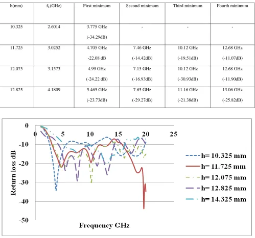
The impedance bandwidth curves for various values of h are shown in Figure 5. The lower edge (f ) of the curves and
various minima for each value of h is given in Table 1. From Table1 and Figure 5 we find that there is a trade off existing between the antenna dimensions and performance. As h increases, the fL (Lower cutoff frequency) of the impedance
bandwidth curve also increases. This is a drawback since as we have to cover the entire UWB. Moreover for this range if the minima are deep (return loss >10 dB) it is meant to be a good design. From Figure 5 we observe that for h= 12.825 mm the dips are low enough when compared with other lines. But by looking at the group delay curves for h=11.725 mm in Figure 7 the optimum value is chosen as h=11.725 mm for which the group delay is constant.
The impedance bandwidth in terms of VSWR (VSWR < 2) for h = 11.725 mm is shown in Figure 6 .a. and in terms of smith chart in Figure 6.b. In both the plots we see that for the UWB range there is a good impedance matching between the patch and the feed as the VSWR value is noted to be less than 2. This is also indicated by the closely packed coils in the smith chart.
5.
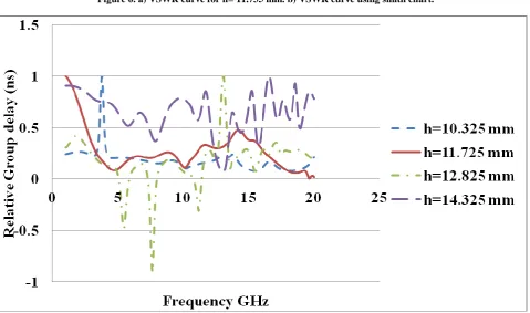
GROUP DELAY
A constant group delay which ensures low dispersion in time domain is required for an UWB antenna. This is an important characteristic of an UWB antenna. The group delay graphs for different values of h are plotted in Figure 5. A constant group delay over the UWB range is got for h= 11.725 mm. Hence h= 11.725 mm is chosen as optimum value in all the graphs.
6.
CURRENT DISTRIBUTION
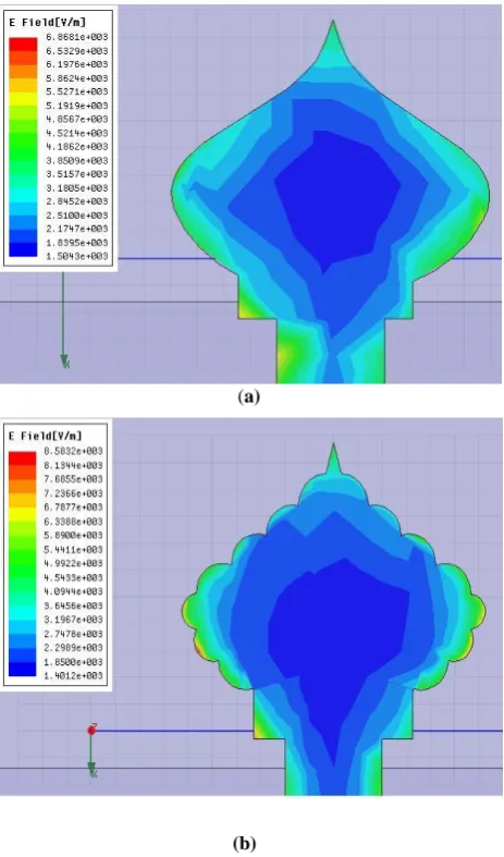
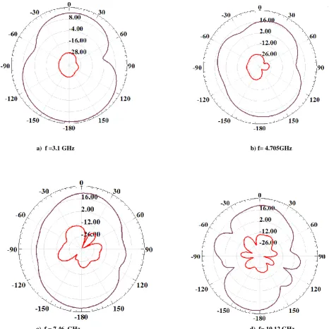
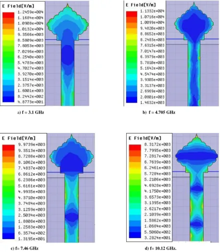
The current distributions for the various minima obtained from the impedance bandwidth curve for h= 11.725 mm is plotted in Figure 11. These minima indicate the resonant frequencies of various modes excited in the patch. As the current distribution varies, different modes are excited. The fact is that these modes have to be excited with closely spaced resonant frequencies so that a wide band is achieved. For h=3.1 GHz there is a gradual variation of the electric field intensity starting from the bottom of the patch to the apex. This behavior can be seen as the formation of parasitic patches being excited along with the main patch with closely spaced resonant frequencies. The magnitude of the electric field components is high around the edges of the patch. These edge components are responsible for the formation of the fringing fields that routes for the formation of omnidirectional radiation pattern seen in Figure 8. For f = 4.705 GHz, 7.46 GHz, 10.12 GHz the variation of the electric field is less around the patches when compared to 3.1GHz and hence this leads to increase in cross polarization levels as seen in figure 8.
[image:3.595.55.287.235.629.2]7.
3D RADIATION PATTERN
[image:3.595.317.479.604.744.2]Table 1. Lower edge frequencies and minima for various values of h.
h(mm) fL(GHz) First minimum Second minimum Third minimum Fourth minimum
10.325 2.6014 3.775 GHz
(-34.29dB)
- - -
11.725 3.0252 4.705 GHz
-22.08 dB
7.46 GHz (-14.42dB)
10.12 GHz (-19.51dB)
12.68 GHz (-11.07dB)
12.075 3.1573 4.99 GHz
(-24.22 dB)
7.15 GHz (-16.93dB)
10.12 GHz (-30.93dB)
12.68 GHz (-11.90dB)
12.825 4.1809 5.465 GHz
(-23.73dB)
7.65 GHz (-29.27dB)
11.16 GHz (-21.38dB)
13.06 GHz (-25.82dB)
Figure 5. Impedance bandwidth curves for various values of h. The most optimum value
8.
PEAK GAIN
The Peak gain in dB is plotted for various frequencies in Figure 9. The peak gain gradually increases within the UWB. The fact that it is a gradual increase is an advantage because a sharp increase in gain would mean a sharp increase in the directivity which in turn results in a sharp degradation of the omnidirectional radiation pattern.
9.
PEAK DIRECTIVITY
The peak directivity in dB is plotted for various frequencies in Figure 10. The peak directivity plot shows similar characteristics as that of the peak gain plot.
a) b )
Figure 6. a) VSWR curve for h= 11.735 mm. b) VSWR curve using smith chart.
[image:5.595.58.523.75.261.2]Figure 7. Relative Group delays for various values of h.
10.
RADIATION PATTERN
[image:5.595.57.537.281.564.2]a) f =3.1 GHz b) f= 4.705GHz
[image:6.595.63.530.73.541.2]
c) f = 7.46 GHz d) f= 10.12 GHz
Figure 8. Elevation Patterns in YZ plane.
Figure 9: Peak gain Vs frequency
[image:6.595.315.543.576.729.2]
a) f = 3.1 GHz b) f = 4.705 GHz
[image:7.595.55.497.107.612.2]
c) f= 7.46 GHz d) f= 10.12 GHz.
Figure 11. Current distribution in the patch for a) f = 3.1GHz b) f = 4.705 GHz c) f = 7.46 GHz d) f = 10.12 GHz
11.
CONCLUSION
A printed antenna that has a shape of a leaf belonging to the class of printed monopole antenna was discussed. Its radiation pattern, impedance bandwidth and surface current distributions were analyzed. The proposed antenna is compact (40mm×40mm) and hence can be incorporated into smaller devices that operate in the UWB range. Since the proposed antenna operates in a very high frequency range it can be used for military purposes.
12.
REFERENCES
[1] Xing Jian, Simin Li and Guangjie Su ,” Broadband planar Antenna with Parasitic Radiator”, Electronic Letters, 13 th Nov 2003 , Vol 39, No 23.
[3] Seong-Youp Suh, Warren L.Stutzman and William A Davis,“A New Ultrawideband Printed Monopole Antenna: The Planar Inverted Cone Antenna(PICA)”, IEEE Transactions on Antenna and Wave Propagation, Vol 52, No.5, May 2004.
[4] Zhi Ning Chen, “Broadband Roll Monopole”, IEEE Transactions on Antenna and Wave Propagation, Vol 51, No.11, November 2003.
[5] M.J. Ammann,Zhi Ning Chen, “Investigation on L-shaped Planar antennas”, Radio Science, Vol.39, RS 2009, doi: 10. 1029/200RS3 .
[6] T.Dong, Y.P Chen “Novel Design of Ultra-Wideband Printed Double-sleeve Monopole Antenna” Progress in Electromagnetics Research Letters, Vol.9, 165-173, 2009.
[7] K.P.Ray “design Aspects of Printed Monopole Antennas for Ultra-wide band Applications” International Journal of Antennas and Propagation Vol 2008, Article ID 133858, Hindawi Publications.
[8] Kamran Ghorbani and Rod B. Waterhouse, “Ultra Broadband Printed Ultra wideband Antenna”, IEEE Transactions on Antennas and Propagation, vol 50, no.12, December 2002.
[9] Abdelnasser A.Eldek, Atef Z.Elsherleni Charles E.Smith,”Wideband Modified Printed Bow-Tie Antenna with single and Dual polarization for C- and X- Band Applications” IEEE Transactions on Antenna and Wave Propagation, Vol 33, No.9, September 2005.
[10] Pengcheng Li, Jianxin Liang, Xiadong Chen“Study of Printed Elliptical/Circular Slot Antennas for Ultrawideband Applications”, IEEE Transactions on Antenna and Wave Propagation, Vol 54, No.6, June 2006.
[11] Yi-Cheng Lin and Kuan-Jung Hung, “Compact Ultrawideband Rectangular Aperture Antenna and Band-Notched designs”, IEEE Transactions on Antenna and Wave Propagation, Vol 54, No.11, November 2006. [12] Wen-Shan Chen, Kuang-Yuan Ku “Band-Rejected
Design of the printed open slot Antenna for WLAN/WiMAX operation”, IEEE Transactions on Antenna and Wave Propagation, Vol 56, No.4, April 2008.
[13] Nicolas Fortino, Jean-Yves Dauvignac, Gerges Kossiavas and Robert Staraj, “Design Optimization of UWB Printed Antenna for Omnidirectional Pulse Radiaton”, IEEE Transactions on Antenna and Wave Propagation, Vol 56, No.7, July 2008.
[14] Reza Zaker, Changiz Ghobadi and Javad Nourinia, “ Bandwidth Enhancement of Novel Compact Single and Dual Band –Notched Printed Monopole Antenna with a pair of L-shaped slots”, IEEE Transactions on Antenna and Wave Propagation, Vol 57, No.12, December 2009. [15] Nan Chang and Jing-Hae Jiang , “Meander Tshaped
Monopole Antenna”, IEEE Transactions on Antenna and Wave Propagation, Vol.57, N0.12, December 2009. [16] K. Gerorge Thomas and M.Sreenivasan, “A simple
Ultra Wideband Planar Rectangular Printed Antenna with Band Dispensation”, IEEE Transactions on Antenna and Wave Propagation, Vol 58, No.1, January 2010.
[17] Jianjun Liu, Shunshi Zhong Karu P. Esselle,” A Printed Elliptical Monopole Antenna with Modified Feeding Structure for Bandwidth Enhancement” IEEE transactions on Antenna and Propagation, vol.59, No.2, Feb 2011.
[18] M.Ojaroudi, Sh. Yazadanifard, N.Ojaroudi, and M.Naser-Moghaddasi,” Small square Monople Antenna with Enhanced BandWidth by using Inverted T-shaped slot and Conductor –Backed Plane”, IEEE Transactions on Antenna and Propagation, vol.59,No.2,Feb 2011.. [19] Mohamed Nabil Srifi, Symon K Podilchak, Mohamed
Essaidi, Yahia M.M. Antar, “Compact Disc Monopole Antennas for Current and Future Ultrawideband (UWB) Applications, IEEE Transactions on Antenna and Propagation, Vol 59, No.12, December 2011.
[20] Rod.B. Waterhouse, S.D/ Targonski, D.M.Kokotoff, “Design and Performance of Small Printed Antennas” IEEE Transactions on Antenna and Propagation, Vol.46, No.11, Nov 1998.
[22] Rajender Singh, “Broadband Planar Monopole Antennas” M.tech Credit Seminar Report, Electronic Systems group, Electrical Department, IIT Bombay, November 2003.
[23] Karlo Costov and Victor Dimitriev., “Planar Monopole Antenna with cuts at the edges and Parasitic Loops,”. Ultra wide band communications Novel trends-Antennas and Propagation, Federal University of Para, Brazil.