http://dx.doi.org/10.4236/cs.2016.73009
How to cite this paper:Senani, R., Singh, A.K., Gupta, A. and Bhaskar, D.R. (2016) Simple Simulated Inductor, Low-Pass/ Band-Pass Filter and Sinusoidal Oscillator Using OTRA. Circuits and Systems, 7, 83-99.
http://dx.doi.org/10.4236/cs.2016.73009
Simple Simulated Inductor,
Low-Pass/Band-Pass Filter and
Sinusoidal Oscillator Using OTRA
Raj Senani
1*, Abdhesh Kumar Singh
2, Ashish Gupta
3, Data Ram Bhaskar
41Division of Electronics and Communication Engineering, Netaji Subhas Institute of Technology, Sector-3, New Delhi, India
2Department of Electronics and Communication Engineering, Sharda University, Greater Noida, India 3Department of Electronics and Communication Engineering, I.T.S. Engineering College, Greater Noida, India 4Department of Electronics and Communication Engineering, Jamia Millia Islamia, New Delhi, India
Received 1 February 2016; accepted 19 March 2016; published 23 March 2016
Copyright © 2016 by authors and Scientific Research Publishing Inc.
This work is licensed under the Creative Commons Attribution International License (CC BY). http://creativecommons.org/licenses/by/4.0/
Abstract
Although a variety of applications of the OTRAs have been reported in literature, the pole of the
transresistance gain Rm of the OTRA has been usually considered to affect the performance of the
circuits due to being parasitic. In this paper, the pole of the OTRA has been used to evolve some simple OTRA-based active-R circuits for realizing a synthetic inductor, single resistance controlled oscillator and low-pass/band-pass filter. The workability of all the proposed circuits has been ve-rified by SPICE simulations and all the new circuits have been found to work as predicted by theory. The exemplary propositions suggest that it is worthwhile to further investigate new circuit designs using OTRA-pole.
Keywords
Operational Transresistance Amplifier, OTRA, Inductance Simulation, Sinusoidal Oscillators, Filters
1. Introduction
Operational Transresistance Amplifier (OTRA) has received a lot of attention over the past decades. Due to
ing a differential current controlled voltage source, it has a virtual ground at both the input terminals, which pro-vides the significant advantages of eliminating parasitics at the input ports. Thus, motivated by these advantages, several CMOS OTRA [1]-[4] architectures have been proposed in the literature and simultaneously, a large va-riety of applications of OTRAs have been evolved so far, such as integrators [5], immittance simulators [6]-[10], oscillators [11]-[26], square/triangular waveform generators [27], monostable/bi-stable multivibrators [28], first and second order all pass filters and biquad filters [29]-[38] etc.
Although the non-ideal one pole and two pole models [39] of transresistance gain (Rm) have been employed by several authors in performing a non-ideal analysis of their propositions but to the best of the knowledge of the authors, any explicit use of OTRA-pole in evolving external capacitor-less, active-R circuits using OTRAs has not been reported so far. The main purpose of this paper is, therefore, to report three OTRA-based active-R circuits which realize an inductor, an oscillator and a low-pas/band-pass filter respectively in which the pole of the OTRA has been exploited advantageously to result in circuits which have the interesting feature of employ-ing a low number of total components. The workability of the proposed circuits has been demonstrated by SPICE simulation results based upon CMOS-OTRA implementation using 0.5 µm CMOS technology.
2. The Proposed Circuits
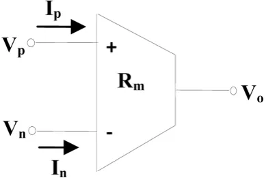
The OTRA can be symbolically shown as in Figure 1, and is characterized by the terminal equation
( )(
)
O m P n
V =R s I −I (1)
The two-pole model of the transresistance [39] of the OTRA is given by
( )
1 2
1 1
o m
p p
R
R s
s s
ω ω
=
+ +
(2)
The above expression for Rm(s) can be further modified and written as-
( )
2
1 1
1
m
p
p o p
R s
s
C s
C R ω
=
+ +
(3)
For frequencies lying in the range: ωp1 ω ωp2, Equation (2) can be approximated as
( )
1m
p
R s
sC
≅ ; where
1
1 p
o p C
Rω
= (4)
Ro is the dc resistance of the OTRA.
2.1. Analysis of the Proposed Circuits Using One-Pole Model of an OTRA
[image:2.595.217.412.570.702.2]Consider now the following:
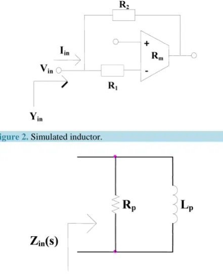
1) For the circuit of Figure 2 straight forward analysis using Rm
( )
s given by Equation (4) shows that the input admittance of the circuit is given respectively by( )
1 2 1 2
1 1 1
in
p
Y s
R R sC R R
= + +
(5)
From Equation (5), we observe that the circuit of Figure 2, thus, realizes a resistance (Rp) in parallel with an inductance (Lp), where Rp =R1R2 and Lp=C R Rp 1 2. The equivalent circuit of which is shown in Figure 3.
The quality factor of the simulated inductor is found using the expression
(
)
1 2
1 2
1 2
1 2
p p
p p
L C R R
Q C R R
R R R
R R
ω ω
ω
= = = +
+
(6)
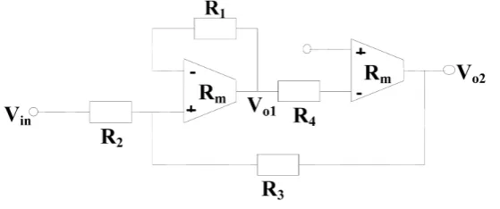
2) In Figure 4 we show the new proposed single-resistance-controlled-oscillator (SRCO) circuit.
[image:3.595.203.424.286.562.2]The straight forward analysis of the proposed circuit using Equation (4) gives the characteristic equation (CE) of the circuit as
Figure 2.Simulated inductor.
Figure 3.Equivalent circuit of simulated inductor.
2 2
3 4 3 4
2 1
1 1
1 0
p p
s C R R sC R R
R R
+ − + =
(7)
It can be easily verified from the CE given by Equation (7) that the condition of oscillation (C.O.) and the frequency of oscillation (F.O.) are respectively given by
1 2
C.O. : R =R (8)
3 4
1 1
F.O. : 2π
o p
f
C R R
= (9)
It may be noted that the circuit offers fully uncoupled CO and FO, the former is adjusted by R1 and/or R2 and the latter may be varied by R3 and/or R4. It may be mentioned that any fully uncoupled oscillator using only four resistors along with only two active elements, that too without using any external capacitors, has not been re-ported in the literature earlier.
3) The last proposition is of an active-R OTRA-based low-pass/band pass filter which has been obtained from the circuit of Figure 4 by changing the polarities of the OTRA terminals and is shown in Figure 5. A straight forward analysis of this circuit using Equation (4) reveals that its transfer functions are given by
3 2
2 3 4
2
2
2
1 3 4
1
1 1
p O
in LP
p p
R
R C R R
V V
s s
C R C R R
−
=
+ +
(10)
1
2 1
1
2
2
1 3 4
1
1 1
p O
in BP
p p
R s
R C R
V V
s s
C R C R R
=
+ +
(11)
where the filter parameters are given by
3 4
1 1
2π
o p
f
C R R
= (12)
1
1
p BW
C R
= (13)
1
2
oBP R H
R
= and 3
2
oLP R H
R
= − (14)
[image:4.595.176.456.591.708.2]A novel feature of the proposed band-pass filter is that all the three filter parameters can be found to be elec-tronically tunable [40]-[44] and can be controlled independently through various resistors: ωo by R3 while the
bandwidth (BW) by R1 and finally, the gain by R2.
2.2. Analysis of the Proposed Circuits Using Two-Pole Model of an OTRA
1) For the circuit of Figure 2 straight forward analysis using Rm
( )
s given by Equation (3) shows that the input admittance of the circuit is given by( )
21 2 1 2 1 2 1 2
1 2
2 2
1 1 1
in
p
p
p p o o
Y s
R R s C R R R R R R
s C R R
R R ω ω = + + + + + (15)
Thus, from Equation (15) the circuit of Figure 2 can be considered as a realization consisting of a resistance (Rp) in parallel with a series combination of a frequency dependent negative capacitance (FDNC), an inductor
and a resistance (Rs) such that RP =R1R2,
1 2
2 p
p
C R R M
ω
= , 1 2
1 2 2
p p
p o
R R
L C R R
R
ω
= +
and
1 2 s o R R R R
= . The
equivalent circuit of which is shown in Figure 6.
The quality factor of the simulated inductor considering all the parasitics is found to be using the expression
1 2
2
1 2 2 2
1
1 p
p o eq
o p p o
s p o p
o
R R C
R L
Q R C C R
R R
R R
R ω
ω
ω ω ω ω
ω ω + = = = + = +
(16)
2) By a straight forward analysis, using Equation (3) we obtain the characteristic equation (CE) of the circuit shown inFigure 4 to be
2 2
3 4 3 4
4 3
2
2 2
2 2
3 4 2 2 2
2 2 2 2 1
3 4 2
2 1 2 2 2 1
2 1
1
4 1 1 1 1
1
1 1 2 2 1 1 1
p p
p p o p
p
p
p o p p o p p p
p
o p o p p o p
C R R C R R
s s
C R
s C R R
C R C R C R R
s C R R
R R R C R C R R R
ω ω
ω
ω ω ω
ω ω + + + + + + − + − + + + − 2 3 4 2 2 1
1 1 1
1 p 0
o p o
C R R
R R R
C R + + − + = (17)
[image:5.595.171.452.385.525.2] [image:5.595.233.390.564.705.2]Neglecting the term s4 and the coefficients involving the term
ω
2p2 the CE given by Equation (17) can besimplified and rewritten as
2 3 4
3 2 2
3 4
2 2 2 2 1
3 4
2 1 2 2 2 1
3 4
2 1
2 4 1 1 1
1
1 1 2 1 1 1 1
1
2
1 1 1
1 0
p
p
p p o p p p
p
o p o p p p
o o
C R R
s s C R R
C R C R R
s C R R
R R R C R C R R
R R
R R R R
ω ω ω
ω ω + + + − + − + + + − + + − + = (18)
Comparing the above equation with the standard form given as
3 2
3 2 1 0 0
a s +a s +a s+a = (19)
we obtain the following values for the coefficients of the Equation (19) as
2 3 4 3
2
2
2 3 4
2 2 2 1
1 3 4
2 1 2 2 2 1
3 4 0
2 1
2
4 1 1 1
1
1 1 2 1 1 1 1
1
2
1 1 1
1 p
p
p
p o p p p
p
o p o p p p
o o
C R R a
a C R R
C R C R R
a C R R
R R R C R C R R
R R a
R R R R
ω ω ω ω ω = = + + − = − + + + − = + − + (20)
For the CE of the form given by (19) the expression for the frequency of oscillation (F.O.) and the condition of oscillation (C.O.) are given respectively as
F.O.: 0
2 1 2π o a f a
= and C.O.: 3 2
1 0
a a
a = a (21)
Thus, for the CE given by (13), the expressions for F.O. and C.O. are found to be
F.O.:
3 4
2 1
2 2 1
1 1 1
1
4 1 1 1 1
1
4
o o
o o
p p o
R R
R R R R
f f
C R R R
ω + − + = + + − (22)
where fo is as given by Equation (9).
C.O.: 2 3 4
2 1 2 2 4 1 1 1 1 1 1 2 o p
p o p p o p
p o
p p
R C
C R C R C R R
R R C R
ω ω ω + − − − ≤ − − (23)
The percentage error in the frequency of oscillation can be found using the expression for percentage error =
o o o f f f −
and the approximate error function is given as
3 4 3 4
2 1 2 2
1 1 1 1 4
%error 100
o p p o o p p
R R R R
R R R C
ω
R R Cω
≅ − − + − ×
3) A straight forward analysis of the circuit shown in Figure 5 using Equation (3) reveals that its transfer function is given by
3 2
2 3 4
2
2 2
2
2 1 2 3 4
1
1 1 1 1
1 1
p O
in LP
p o p p p o p p
R
R C R R
V
V s s
s s
C R ω C R C R ω C R R
− = + + + + + + (25) 1
2 1 2
1
2 2
2
2 1 2 3 4
1 1
1
1 1 1 1
1 1
p p o p
O
in BP
p o p p p o p p
R s
s
R C R C R
V
V s s
s s
C R C R C R C R R
ω ω ω + + = + + + + + + (26)
Equations (25) and (26) on neglecting the terms containing s4 and s3 can be simplified and the modified trans-fer functions are thus obtained as follows
3 4
1 3
2
2 3 4 3 4 1
1 2 1
2 1 2 2 2 1 1 2 1 1 1 1 4 1
1 1 1
2 1 1 1 1 1 4 1 1 1 o p
o p p o
O
in LP
o p p o
p p
p p o
R R R R R
R R R C R R R
R R C R R
V
V R
R C R
s s
C R R C
C R R
ω ω ω + − + + + = + + + + + + 3 4 1
3 4 1
2 1 1 4 1 1 1 o
p p o
R R R R
R R R
C R R
ω + + + (27) 1 2 1
2 1 1 1
2 1 1 1 2 2 1 1 2 1 2 1 1 1 1
2 1 4
1 1 2 1 1 1 1 4 1 1 1
o p p o
o
o p
p p o
O
in BP
o p p o
p
p p o
R
R C R
R R
s
R R R C R R
C R R
V
V R
R C R
s s
C R R
C R R
ω ω ω ω + + + + + = + + + + + 3 4 1 2
3 4 1
2 1 1 1 4 1 1 1 o p
p p o
R R R R
C R R R
C R R
ω + + + + (28)
From Equations (27) and (28) we obtain the expressions for the filter parameters as
1 3 4 2 1 * * 1 1
2 1 2 1
1 2 1 * * 1 2 1 1 1 1 , 4 4 1 1
1 1 1 1
4 1 1 1 , 2 1
o p p o
o
o o
p p o p p o
oLP
p p o
oBP
oBP oLP
o
R R R
R C R
R R
f f BW BW
R R
C R R C R R
R H
C R R
H H H R R ω ω ω ω + + + = = + + + + + + = = + 3 4 3 1 1 o o
R R R
R R R
where fo, BW, HoBP and HoLP are given respectively by Equations (12), (13) and (14).
3. SPICE Simulation Results
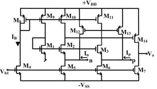
[image:8.595.180.453.260.414.2]All the three proposed circuits have been verified through SPICE version 16.0 simulations using CMOS OTRA of [4] reproduced herein Figure 7 where the aspect ratios of MOSFETs are as given in Table 1 and the model parameters using 0.5 µm CMOS technology provided by MOSIS (AGILENT) are as given in Table 2.
Figure 8 and Figure 9 show the variation of Rp and Lp respectively as compared to their theoretical plots. The proposed inductor was simulated using the component values as R1 = 2.2 KΩ, R2 = 3.3 KΩ and Cp = 1.2 pF re-sulting in the theoretical value of Rp = 1.32 KΩ and Lp = 8.71 µH which are in close agreement with the simu-lated values of Rp = 1.34 KΩ and Lp = 8 µH.
[image:8.595.94.537.437.703.2]The simulated lossy inductor of Figure 2 can be used to realize a band pass filter circuit as shown in Figure 10. A straight forward analysis of the circuit results in the following expression of the transfer function of the circuit.
Figure 7.An exemplary CMOS Implementation of an OTRA [4].
Figure 8. Variation of Rp with respect to frequency.
100 101 102 103 104 105 106 107 108 109 1010
-20000 -15000 -10000 -5000 0 5000
Frequency (Hz)
Re
Figure 9. Variation of Leq with respect to frequency.
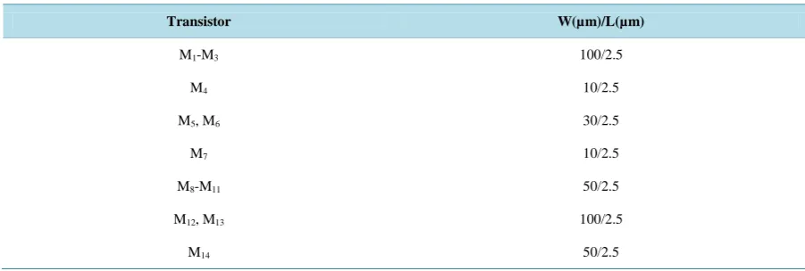
Table 1. Aspect ratios of the various MOSFETs for the circuit of Figure 7[4].
Transistor W(µm)/L(µm)
M1-M3 100/2.5
M4 10/2.5
M5, M6 30/2.5
M7 10/2.5
M8-M11 50/2.5
M12, M13 100/2.5
[image:9.595.85.536.392.544.2]M14 50/2.5
Table 2.Model parameters of NMOS and PMOS transistors.
Device
Type Model Parameters
NMOS
LEVEL = 3 UO = 460.5 TOX = 1.0E−8 TPG = 1 VTO = 0.62 JS = 1.08E−6 XJ = 0.15E−6 RS = 417 RSH = 2.73 LD = 4E−8 VMAX = 130E3 NSUB = 1.71E17 PB = 0.761 ETA = 0.00 THETA = 0.129 PHI = 0.905 GAMMA = 0.69 KAPPA = 0.10 CJ = 76.4E−5 MJ = 0.357 CJSW = 5.68E−10 MJSW = 0.302 CGSO = 1.38E−10 CGDO = 1.38E−10 CGBO = 3.45E−10 KF = 3.07E−28 AF = 1 WD = 1.1E−7 DELTA = 0.42 NFS = 1.2E11
PMOS
LEVEL = 3 UO = 100 TOX = 1.0E−8 TPG = 1 VTO = −0.58 JS = 0.38E−6 XJ = 0.10E−6 RS = 886 RSH = 1.81 LD = 3E−8 VMAX = 113E3 NSUB = 2.08E17 PB = 0.911 ETA = 0.00 THETA = 0.120 PHI = 0.905 GAMMA = 0.76 KAPPA = 2 CJ = 85E−5 MJ = 0.429 CJSW = 4.67E−10 MJSW = 0.631 CGSO = 1.38E−10 CGDO = 1.38E−10 CGBO = 3.45E−10 KF = 1.08E−28 AF = 1 WD = 1.4E−7 DELTA = 0.81 NFS = 0.52E11
100 101 102 103 104 105 106 107 108 109 1010
-1 0 1 2 3 4 5 6
7x 10
-5
Frequency (Hz)
Le
2 1
p p o
p o o o p
o
in BP p o
o o p o p
R R R
s
R R C R R
V
V R R
s s
C R R C L
+ + = + + + (30)
For the band pass filter shown in Figure 10 we obtain the following filter parameters:
(
)
(
)
(
)
1 2
1 2 1 2
1 2 1 2 1 2
1 2 1 2
1 2 1 2 1 1 2π 2π p o
o p o
o p o o o
o p p o p
o p o
o
o o p o o
o
o p o p
R R R
H
R R R R R R R
R R C R C
Q
R R L R R R R R C R R
R R R R R R R
Q C R R C R R R
f
C L C C R R
ω = = + + + = = + + + + + + = = = = (31)
Considering the equivalent circuit of Figure 6 and using it to realize a band pass filter circuit we obtain the transfer function given by
2
3 2
1
1 1 1
p s
o o o o o o
o
in p p p s s s
o o o p o o o p o o o p o
L R
s s
C R MC R MC R
V
V L L L R R R
s s s
C R C R M MC R MC R M MC R MC R MC
+ + = + + + + + + + + + (32)
The above equation can be simplified and written as
(
)
(
(
)
)
(
)
(
)
(
(
)
)
2
p p o o s o p
p p
p p o o s o p p o o p o p
o
in p p o o s o p s p o o p
p o o p o p p o o p o p
L R R C R R R
L R
s
L R R C R R R M R R C L R R
V
V L R R C R R R R R R R R
s s
M R R C L R R M R R C L R R
+ + + + + + = + + + + + + + + + + (33)
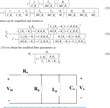
From Equation (33) we obtain the modified filter parameters as
* 1 o o o p o s
p o p
H H
R R C R
L R R
[image:10.595.156.539.341.714.2]= + + (34)
(
)
(
)
* 1
1
o s o p
p o p
o o
o p
o p o p C R R R
L R R
Q Q M R R
C L R R
ω ω
+
+
=
+
+
(35)
(
)
(
)
*
1
1
s o p
o p
o o
o p
o p o p
R R R
R R
f f
M R R
C L R R
+
+
=
+
+
(36)
where, Ho, o Q ω
[image:11.595.158.538.81.245.2] and fo are respectively given by Equation (31).
Figure 11 shows the simulated result of the band pass filter circuit shown in Figure 10 (an application exam-ple of simulated inductor). The circuit was simulated with the choice of components as follows: Ro = Rp = 1.32 KΩ, Lp = 8.712 µH, Co = 4.65 pF resulting in theoretical value of filter parameters as-Ho = 0.5, BW = 326 MHz and fo = 25 MHz as compared to the simulated values Ho = 0.499, BW = 325.7 MHz and fo = 25.16 MHz.
Figure 12 shows the transient response of the proposed oscillator circuit shown in Figure 4 with the compo-nent values as R1 = 25.01 KΩ, R2 = 25 KΩ, R3 = R4 = 30 KΩ and Cp = 1.2 pF resulting in theoretical value of oscillation frequency fo = 4.42 MHz which agrees with the simulated result of fo = 4.45 MHz.
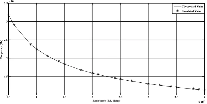
Figure 13 and Figure 14 show the variation of oscillation frequency with respect to R3 and R4 when the val-ues of the resistances R3 and R4 are respectively varied from 5 KΩ to 40 KΩ.
For the component values chosen as R1 = 25.01 KΩ, R2 = 25 KΩ, R3 = R4 = 30 KΩ, Cp = 1.2 pF, Ro = 126 MΩ and ω =p2 95.9 Mrad sec, using Equations (9) and (22) respectively the oscillation frequency is found to be fo = 4.42 MHz using one-pole model and fo = 4.485 MHz using two-pole model resulting in the percentage error of 1.47%.
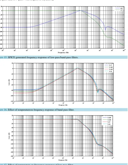
Figure 15 shows the SPICE generated frequency response of the band-pass filter with component values chosen as R2 = R3 = R4 = 47 KΩ, R1 = 300 KΩ and Cp = 1.2 pF resulting in theoretical values of fo = 2.82 MHz and BW = 2.78 MHZ which is in accordance with the simulated values of fo = 2.8363 MHz, BW = 2.7554 MHz.
Figure 11. Simulation result of Band pass filter.
100 101 102 103 104 105 106 107 108 109 1010
0 0.1 0.2 0.3 0.4 0.5 0.6 0.7
Frequency (Hz)
M
a
g
ni
tude
[image:11.595.90.532.466.703.2]Figure 12. Transient response of the proposed SRCO.
Figure 13. Variation of the oscillation frequency with R3.
Figure 14. Variation of the oscillation frequency with R4.
0 0.1 0.2 0.3 0.4 0.5 0.6 0.7 0.8 0.9 1
x 10-4
-2.5 -2 -1.5 -1 -0.5 0 0.5 1 1.5 2 2.5
Time (sec)
O
u
tp
u
t V
o
lta
g
e
(V
)
0.5 1 1.5 2 2.5 3 3.5 4
x 104 0.8
1 1.2 1.4 1.6 1.8 2 2.2 2.4 2.6 2.8x 10
6
Resistance (R3, ohms)
F
req
u
en
cy
(
H
z)
Theoretical Value Simulated Value
0.5 1 1.5 2 2.5 3 3.5 4
x 104 1
1.5 2 2.5 3 3.5x 10
6
Resistance (R4, ohms)
F
req
u
en
cy
(
H
z)
Theoretical Value
[image:12.595.136.490.521.699.2]Figure 16 and Figure 17 shows the effect of temperature variations on the frequency response of the band pass and low pass filter when the temperature is varied from 10˚C to 100˚C.
[image:13.595.86.534.180.371.2]Figure 18 shows the variation of gain of band pass filter with resistance R2 when its value is varied from 280 Ω to 320 KΩ and Figure 19 shows the variation of gain of low pass filter with resistance R3 when its value is varied from 40 KΩ to 80 KΩ. Thus, Figure 18 and Figure 19 respectively show the variability of gain for band-pass and low-pass with respect to R2 and R4.
[image:13.595.121.534.429.702.2]Figure 15. SPICE generated frequency response of low-pass/band-pass filters.
Figure 16.Effect of temperatureon frequency response of band-pass filter.
Figure 17.Effect of temperature on frequency response of low-pass filter.
100 101 102 103 104 105 106 107 108 109 1010 -180
-160 -140 -120 -100 -80 -60 -40 -20 0 20
Frequency (Hz)
Ga
in
(
d
B
)
BPF
LPF
100 101 102 103 104 105 106 107 108 109 1010
-120 -100 -80 -60 -40 -20 0 20
Frequency (Hz)
Ga
in
(
d
B
)
T=27 T=100 T=200 T=10
100 101 102 103 104 105 106 107 108 109 1010
-180 -160 -140 -120 -100 -80 -60 -40 -20 0 20
Frequency (Hz)
Ga
in
(
d
B
)
Figure 20 and Figure 21 respectively shows the simulation results of the band pass and the low pass response of the circuit shown in Figure 5 considering the one-pole , two-pole model of the OTRA and the SPICE result.
It can be seen that the results obtained from SPICE simulations demonstrate good correspondence with the theoretical values, which confirms the workability of the proposed circuits.
[image:14.595.129.495.470.703.2]Figure 18. Variation of gain with R2 for the band-pass filter.
Figure 19. Variation of gain with R4 for the low-pass filter.
Figure 20.Simulation result of band-pass filter.
100 101 102 103 104 105 106 107 108 109 1010 -120
-100 -80 -60 -40 -20 0 20
Frequency (Hz)
Ga
in
(
d
B
)
100 101 102 103 104 105 106 107 108 109 1010 -180
-160 -140 -120 -100 -80 -60 -40 -20 0 20
Frequency (Hz)
Ga
in
(
d
B
)
100 101 102 103 104 105 106 107 108 109 1010 0
0.2 0.4 0.6 0.8 1 1.2 1.4
Frequency (Hz)
M
a
g
ni
tude
Figure 21.Simulation result of low-pass filter.
4. Concluding Remarks
Three simple circuits using OTRA-pole were proposed: a simulated inductance, a fully uncoupled SRCO and a low-pass/band-pass filter. In these circuits the pole of the OTRA has been exploited advantageously to result in circuits which have the interesting feature of employing a low number of total components. The theory has been validated by SPICE simulation results. The workability of the proposed circuits, thus, demonstrates that the de-sign of active-R circuits using OTRA-pole warrants further investigations.
Acknowledgements
This work was performed partly at Analog Signal Processing Research Lab., Division of ECE, NSIT, New Delhi and partly at Advanced Analog Signal Processing Lab., Department of ECE, Faculty of Engineering and Tech-nology, Jamia Millia Islamia, New Delhi.
References
[1] Chen, J.J., Tsao, H.W. and Chen, C. (1992) Operational Transresistance Amplifier Using CMOS Technology.
Elec-tronics Letters, 28, 2087-2088. http://dx.doi.org/10.1049/el:19921338
[2] Chen, J.J., Tsao, H.W., Liu, S. and Chui, W. (1995) Parasitic Capacitance Insensitive Current-Mode Filters Using
Op-erational Transresistance Amplifier. IEE Proceedings—Circuits, Devices and Systems, 142, 186-192.
[3] Chen, J.J., Tsao, H.W. and Liu, S.I. (2001) Voltage-Mode MOSFET-C Filters Using Operational Transresistance
Am-plifiers (OTRAs) with Reduced Parasitic Capacitance Effect. IEE Proceedings—Circuits, Devices and Systems, 148,
242-249.
[4] Hassan, H.M. and Soliman, A.M. (2006) A Modified CMOS Realization of the Operational Transresistance Amplifier
(OTRA). Frequenz, 60, 70-76.
[5] Chiu, W., Tsay, J.H., Liu, S.I., Tsao, H.W. and Chen, J.J. (1995) Single Capacitor MOSFET-C Integrator Using OTRA.
Electronics Letters, 31, 1796-1797. http://dx.doi.org/10.1049/el:19951283
[6] Çam, U., Kacar, F., Çiçekoğlu, O., Kuntman, H. and Kuntman, A. (2003) Novel Grounded Parallel Immittance
Simu-lator Topologies Employing Single OTRA. International Journal of Electronics and Communications (AEU), 57, 287-
290. http://dx.doi.org/10.1078/1434-8411-54100173
[7] Çam, U., Kacar, F., Cicekoglu, O., Kuntman, H. and Kuntman, A. (2004) Novel Two OTRA-Based Grounded
Immit-tance Simulator Topologies. Analog Integrated Circuits and Signal Processing, 39, 169-175.
http://dx.doi.org/10.1023/B:ALOG.0000024064.73784.58
[8] Gupta, A., Senani, R., Bhaskar, D.R. and Singh, A.K. (2012) OTRA-Based Grounded-FDNR and Grounded-Induc-
tance Simulators and Their Applications. Circuits, Systems and Signal Processing, 31, 489-499.
http://dx.doi.org/10.1007/s00034-011-9345-2
[9] Kilinc, S., Salama, K.N. and Cam, U. (2006) Realization of Fully Controllable Negative Inductance with Single
Opera-tional Transresistance Amplifier. Circuits, Systems and Signal Processing, 35, 47-57.
http://dx.doi.org/10.1007/s00034-004-0706-y
[10] Pandey, R., Pandey, N., Paul, S.K., Singh, A., Sriram, B. and Trivedi, K. (2011) New Topologies of Lossless
100 101 102 103 104 105 106 107 108 109 1010
0 0.2 0.4 0.6 0.8 1 1.2 1.4
Frequency (Hz)
M
a
g
ni
tude
Grounded Inductor Using OTRA. Journal of Electrical and Computer Engineering, 2011, Article ID: 175130.
http://dx.doi.org/10.1155/2011/175130
[11] Çam, U. (2002) A Novel Single-Resistance-Controlled Sinusoidal Oscillator Employing Single Operational
Transre-sistance Amplifier. Analog Integrated Circuits and Signal Processing, 32, 183-186.
http://dx.doi.org/10.1023/A:1019586328253
[12] Hou, C.L., Huang, C.C. and Horng, J. W. (2007) A Criterion of a Multi-Loop Oscillator Circuit. Journal of Circuits,
Systems and Computers, 16, 105-111. http://dx.doi.org/10.1142/S0218126607003460
[13] Salama, K.N. and Soliman, A.M. (1999) CMOS Operational Transresistance Amplifier for Analog Signal Processing.
Microelectronics Journal, 30, 235-245. http://dx.doi.org/10.1016/S0026-2692(98)00112-8
[14] Salama, K.N. and Soliman, A.M. (2000) Active RC Applications of the Operational Transresistance Amplifiers.
Fre-quenz, 54, 171-176. http://dx.doi.org/10.1515/freq.2000.54.7-8.171
[15] Salama, K.N. and Soliman, A.M. (2000) Novel Oscillators Using Operational Transresistance Amplifier.
Microelec-tronics Journal, 31, 39-47. http://dx.doi.org/10.1016/S0026-2692(99)00087-7
[16] Chien, H.C. (2014) New Realizations of Single OTRA-Based Sinusoidal Oscillators. Active and Passive Electronic
Components, 2014,Article ID: 938987.
[17] Avireni, S. and Pittala, C.S. (2014) Grounded Resistance/Capacitance-Controlled Sinusoidal Oscillators Using
Opera-tional Transresistance Amplifier. WSEAS Transactions on Circuits and Systems, 13, 145-152.
[18] Pandey, R., Pandey, N., Bothra, M. and Paul, S.K. (2011) Operational Transresistance Amplifier-Based Multiphase
Sinusoidal Oscillators. Journal of Electrical and Computer Engineering, 2011, Article ID: 586853.
[19] Pandey, R., Pandey, N., Kumar, R. and Solanki, G. (2010) A Novel OTRA Based Oscillator with Non Interactive
Con-trol. International Conference on Communication and Computer Technology (ICCCT’10),17-19 September 2010,
Al-lahabad, 658-660. http://dx.doi.org/10.1109/iccct.2010.5640448
[20] Pandey, R., Pandey, N. and Paul, S.K. (2012) MOS-C Third Order Quadrature Oscillator using OTRA. 3rd
Interna-tional Conference on Communication and Computer Technology (ICCCT’12),23-25 November 2012, Allahabad, 77-
80. http://dx.doi.org/10.1109/iccct.2012.24
[21] Pandey, R., Pandey, N., Komanapalli, G. and Anurag, R. (2014) OTRA Based Voltage Mode Third Order Quadrature
Oscillator. ISRN Electronics, 2014, Article ID: 126471. http://dx.doi.org/10.1155/2014/126471
[22] Kumngern, M. and Kansiri, I. (2014) Single-Element Control Third-Order Quadrature Oscillator Using OTRA’s. 12th
International Conference on ICT and Knowledge Engineering,Bangkok, 18-21 November 2014, 24-27.
[23] Pandey, R. and Bothra, M. (2009) Multiphase Sinusoidal Oscillators Using Operational Trans-Resistance Amplifier.
IEEE Symposium on Industrial Electronics and Applications, 1, 371-376. http://dx.doi.org/10.1109/isiea.2009.5356432
[24] Torteanchai, U., Phatsornsiri, P. and Kumngern, M.,(2016) Quadrature Oscillator Using Operational Transresistance
Amplifiers. 7th International Conference on Intelligent Systems, Modelling and Simulation (ISMS), Bangkok, 25-27
January 2016, 403-406.
[25] Pandey, R., Pandey, N., Komanapalli, G., Singh, A.K. and Anurag, R. (2015) New Realizations of OTRA Based
Sinu-soidal Oscillator. 2nd International Conference on Signal Processing and Integrated Networks (SPIN), Noida, 19-20
February 2015, 913-916. http://dx.doi.org/10.1109/spin.2015.7095323
[26] Soliman, A.M. (2013) Two Integrator Loop Quadrature Oscillators: A Review. Journal of Advanced Research, 4, 1-11.
http://dx.doi.org/10.1016/j.jare.2012.03.001
[27] Hou, C.L., Chien, H.C. and Lo, Y.K. (2005) Square Wave Generators Employing OTRAs. IEE Proceedings-Circuits,
Devices and Systems, 152, 718-722. http://dx.doi.org/10.1049/ip-cds:20045167
[28] Lo, Y.K. and Chien, H.C. (2005) Current Mode Monostable Multivibrators Using OTRAs. IEEE Transactions on
Cir-cuits and Systems-II, 53, 1274-1278. http://dx.doi.org/10.1109/TCSII.2006.882361
[29] Cakir, C., Cam, U. and Cicekoglu, O. (2005) Novel All Pass Filter Configuration Employing Single OTRA. IEEE
Transactions on Circuits and Systems-II, 52, 122-125. http://dx.doi.org/10.1109/TCSII.2004.842055
[30] Çam, U., Cakir, C. and Cicekoglu, O. (2004) Novel Transimpedance Type First-Order All Pass Filter Employing
Sin-gle OTRA. International Journal of Electronics and Communications (AEU), 58, 296-298.
http://dx.doi.org/10.1078/1434-8411-54100246
[31] Hwang, Y.S., Wu, D.S., Chen, J.J., Shih, C.C. and Chou, W.S. (2007) Realization of Higher-Order MOSFET-C Active
Filters Using OTRA. Circuits, Systems and signal Processing, 26, 281-291.
http://dx.doi.org/10.1007/s00034-006-0330-0
[32] Kilinc, S. and Cam, U. (2005) Realization of nth-Order Voltage Transfer Function Using a Single Operational
[33] Kilinc, S. and Cam, U. (2006) Transimpedance Type Fully Integrated Biquadratic Filters Using Operational
Transre-sistance Amplifiers. Analog Integrated Circuits and Signal Processing, 47, 193-198.
http://dx.doi.org/10.1007/s10470-006-2963-0
[34] Kilinc, S., Keskin, A.U. and Cam, U. (2007) Cascadable Voltage-Mode Multifunction Biquad Employing OTRA.
Frequenz, 61, 84-86. http://dx.doi.org/10.1515/FREQ.2007.61.3-4.84
[35] Salama, K.N. and Soliman, A.M. (1999) Universal Filters Using the operational Transresistance Amplifiers.
Interna-tional Journal of Electronics and Communications (AEU), 53, 49-52.
[36] Soliman, A.M. (2008) History and Progress of the Tow-Thomas Biquadratic Filter Part-II: Using OTRA, CCII, and
DVCC Realizations. Journal of Circuits, Systems and Computers, 17, 797-826.
http://dx.doi.org/10.1142/S0218126608004691
[37] Soliman, A.M. and Madian, A.H. (2009) MOS-C Tow-Thomas Filters Using Voltage Op-Amp, Current Feedback Op-
Amp and Operational Transresistance Amplifier. Journal of Circuits, Systems and Computers, 18, 151-179.
http://dx.doi.org/10.1142/S0218126609004995
[38] Soliman, A.M. and Madian, A.H. (2009) MOS-C KHN Filter Using Voltage Op-Amp, Current Feedback Op-Amp,
Operational Transresistance Amplifier and DCVC. Journal of Circuits, Systems and Computers, 18, 733-769.
http://dx.doi.org/10.1142/S021812660900523X
[39] Sanchez-Lopez, C., Martinez-Romero, E. and Tlelo-Cuautle, E. (2011) Symbolic Analysis of OTRAs-Based Circuits.
Journal of Applied Research and Technology, 9, 69-80.
[40] Banu, M. and Tsividis, Y. (1982) Floating Voltage-Controlled Resistors in CMOS Technology. Electronics Letters, 18,
678-679. http://dx.doi.org/10.1049/el:19820461
[41] Carlosena, A., Muller, D. and Moschytz, G.S. (1992) Resistively Variable Capacitor Using General Impedance
Con-vertors. IEE Proceedings G (Circuits, Devices and Systems), 139, 507-516. http://dx.doi.org/10.1049/ip-g-2.1992.0080
[42] Senani, R. (1994) Realization of Linear Voltage-Controlled Resistance in Floating Form. Electronics Letters, 30,
1909-1911. http://dx.doi.org/10.1049/el:19941313
[43] Abuelma’atti, M.T. and Khan, M.H. (1995) On the Stability of Resistively Variable Capacitors Using General
Imped-ance Converters. Active and Passive Electronic Components, 18, 129-135. http://dx.doi.org/10.1155/1995/39168
[44] Al-Shahrani, S.M. (2007) CMOS Wide-Band Auto-Tuning Phase Shifter Circuit. Electronics Letters, 43, 804-805.