Variable-height scanning tunneling spectroscopy for local density of states recovery based
on the one-dimensional WKB approximation
B. Naydenov
*
and John J. BolandSchool of Chemistry and Center for Research on Adaptive Nanostructures and Nanodevices (CRANN), Trinity College Dublin, Dublin 2, Ireland
共Received 10 September 2010; revised manuscript received 16 October 2010; published 9 December 2010兲
We introduce a variable-height scanning tunneling spectroscopy共VH-STS兲 method that provides a good
level of recovery of the combined surface and tip density of states 共DOS兲 in any bias range without the
complexity of previous methods. The combined local electron DOS共LDOS兲recovery was performed using a
simplified algorithm based on the one-dimensional Wentzel-Kramers-Brillouin approximation already known in the literature. On the basis of this VH-STS approach we derive three separate methods for the determination of tunnel barrier height and absolute tip-surface separation, and which are critical to enabling LDOS recovery.
We report experimental results on polycrystalline-Pt and Si共100兲surfaces using this scheme. Experimental and
simulated spectra are compared to investigate the limits of the various methods and to demonstrate that this approach can be applied successfully to all kind of probes and surfaces.
DOI:10.1103/PhysRevB.82.245411 PACS number共s兲: 68.37.Ef, 73.20.At
I. INTRODUCTION
Spectroscopy with atomic resolution has been one of the most attractive and challenging outcomes of the invention of the scanning tunneling microscope 共STM兲.1 The accuracy
and reproducibility of the acquired scanning tunneling spec-troscopic 共STS兲 data have improved dramatically since the development of the cryogenic STM. Despite the fact that the local electron density of states 共LDOS兲 has been the main STS objective, until recently there were no significant theo-retical efforts to recover this fundamental property from STS measurements of the tunneling current I共V兲 and differential conductancedI共V兲/dV. The quantity共dI/dV兲/共I/V兲 共Ref.2兲
is still widely used as an estimate of the LDOS although it is clear that it is a rather poor approximation3 and is not
tip-sample distance invariant contrary to recent reports.4 In
the past several years there were significant theoretical studies5–12 involving schemes for LDOS deconvolution
from the STS data based on the one-dimensional Wentzel-Kramers-Brillouin 共1D-WKB兲 approximation. These algo-rithms, recently summarized by Passoniet al.11have led to a
better understanding of the STS experiment but they have not yet been widely adopted in the experimental studies.13
The reason for this is the considerable computational effort required coupled with the need for very accurate data and the fact that a knowledge of two nondirectly measurable quanti-ties共tunneling barrier height and absolute tip-surface separa-tion兲are required for LDOS recovery. Thus to benefit from the full potential of the recovery scheme efforts should be made to acquire good quality data over the entire energy range and to develop a simple and fast data processing pro-cedures for parameter determination.
Here we introduce and describe a variable-height scan-ning tunneling spectroscopy 共VH-STS兲 scheme which has the particular advantage that it allows the signal-to-noise ra-tio to be adjusted over the entire measured energy range. The VH-STS serves as platform for a procedure to obtain the combined tip-sample LDOS recovery based on the 1D-WKB theory. Based on the VH-STS approach we derive共Sec. III兲
three separate methods 共⌽ⴱ, zⴱ, and ⌬R1,2methods兲for the
determination of tunneling barrier and tunneling distance, which, in turn, provide separate information about the tip and the sample electronic structures. We test the limits of these various methods and the recovery scheme, in general, on simulated共Sec.IV兲and experimental data共Sec.V兲. We dem-onstrate that the ⌬R1,2 method is applicable to all type of probes and surfaces and provides a topographic map with a directly observable local minimum calculated from spectro-scopic data at a single-bias value. This minimum provides an accurate estimate of both the work function and the absolute tip-sample separation which are critical for combined LDOS recovery and clearly distinguishes our approach from similar methods published in the literature.10–12The⌽ⴱandzⴱ
meth-ods, although not applicable to all samples and probes, still provide very useful information about underlying surface phenomena and probe electronic structure which can be used for data modeling 共Sec. VI兲 and ultimately to isolate the surface LDOS from the combined tip and sample LDOS.
II. EXPERIMENTAL LAYOUT
Experiments were performed using a Createc cryogenic STM operating at 5 and 77 K. The UHV system in-cludes: analysis, preparation, and load-lock chambers with base pressures ⬍1⫻10−11 mbar, 2⫻10−11 mbar, and
6⫻10−11 mbar, respectively. A cryogenic manipulator pro-vided controlled conditions throughout the whole process of sample preparation and transfer to the microscope. Metal
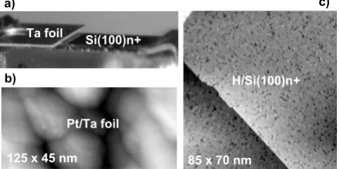
共polycrystalline Pt兲and semiconductor 关Si共100兲n+兴samples were mounted on a dual-sample holder shown in Fig. 1共a兲. Access to both surfaces is provided in the microscope with-out sample exchange. Both samples can be prepared sepa-rately and topographic images demonstrating the quality of the surfaces are presented also in Figs.1共b兲and1共c兲.
Tungsten probes ware annealedin situand inked14on the
with the feedback off. The spectroscopy was performed by choosing a spatial set point, switching the feedback off and ramping the bias 共V兲 and the tip-sample separation 共z兲 through a set of programmed values while recording simul-taneously the tunneling current and its derivative over the bias. An external lock-in amplifier was used for the bias modulation共590 Hz, 20 mV rms兲and the current derivative detection. In every spectrum the bias and the separation were changed forward and backward to ensure that no time hys-teresis exists in the recorded channels. Prior to the spectros-copy measurement key values for the tip-sample separation were obtained by simultaneous multiple-bias imaging of the surface area under investigation so as to define the tip-sample-bias spectroscopic trajectories. These z values were then programmed in the VH-STS parameters together with the corresponding biases. The latter was sufficient to avoid any tip and/or surface modifications during the experiment. All experiments were performed at liquid-nitrogen tempera-tures.
III. THEORETICAL LAYOUT
In the scanning tunneling spectroscopy the principally measured quantity is the tunneling current I共V兲 which is commonly expressed5–12in the form
I共V兲⬀
冕
0 eV
S共兲t共−eV兲T共,eV,z兲d, 共1兲
whereSandtare the sample and tip LDOSs, respectively,
Vis the bias, andzis the separation between the sample and the probe. Tis the barrier transmission coefficient which in the 1D-WKB trapezoidal approximation can be expressed as
T共,eV,z兲= exp
冉
−␣z冑
⌽+eV2 −
冊
. 共2兲 Here⌽ is the tunneling barrier height and␣= 2冑
2m/ប.Following Koslowski et al.7,10 the second STS quantity,
namely, the differential conductance dI/dV共V兲 can be
de-rived from Eqs. 共1兲 and 共2兲 and applying the mean-value theorem for integrals it has the form
dI共V兲
dV =S共V兲t共0兲T共eV,eV,z兲− ␣z 
冑⌽
I共V兲+
冕
0 eV
S共兲T共,eV,z兲
dt共−eV兲
dV d, 共3兲
where the constant⬇4.7Equation共3兲can be rearranged as follows:
S共V兲BT=
冋
dI共V兲
dV +
␣z

冑⌽
I共V兲册
/T共eV,eV,z兲, 共4兲 whereBTis given byBT=t共0兲+
冕
0 eVPS,T共,eV兲
dt共−eV兲
dV d 共5兲
and
PS,T共,eV兲=
S共兲
S共V兲
T共,eV,z兲
T共eV,eV,z兲. 共6兲
IfS共兲is changing slowly compared with the exponentT共兲
then one can make the approximation
PS,T共,eV兲 ⬵const. = 1. 共7兲
Additionally if we replace dt共−eV兲/dV with −dt共 −eV兲/d in Eq. 共5兲, this equation is reduced to BT⬵t共−V兲
and Eq.共4兲can then be rewritten as
S,t共V兲=S共V兲t共−V兲 ⬵
冋
dI共V兲
dV +
␣z

冑⌽
I共V兲册
/T共eV,eV,z兲.共8兲 For a tip with a flat LDOS the left-hand side of Eq. 共8兲
becomes S共V兲t共0兲 as described earlier in the work of Ko-slowski et al.7 On the right-hand side of Eq. 共8兲 the key unknown parameters are the separation z and the barrier height ⌽. Koslowski et al.10 demonstrated that
measure-ments with two significantly different separations can be used as a basis for the tip and sample LDOS recovery by solving a set of integrodifferential equations employing the Neumann approximation scheme. Here we suggest instead thatzand⌽can be determined by applying only Eq.共8兲for two variable-height scanning tunneling spectra measuring I共V兲 and dI/dV共V兲. If the absolute separation is z0 and de-fined for a given bias V0and current I0 one can design two
measurements using predetermined separations z1共V兲=z0
+⌬z1共V兲 andz2共V兲=z0+⌬z2共V兲. The four acquired spectra,
I共V兲anddI/dV共V兲measured atz1andz2are expected to give equal products when applied in Eq. 共8兲, namely, the recov-ered LDOS should be identical for measurements at both separations
S,t共V,z1兲 ⬅S,t共V,z2兲. 共9兲
At zero bias共V= 0兲the current is zero and one can determine from Eqs. 共8兲and共9兲that the barrier height is given by 85 x 70 nm
Ta foil
Si(100)n+
H/Si(100)n+ a)
b)
c)
[image:2.609.53.294.72.192.2]125 x 45 nm Pt/Ta foil
FIG. 1. Sample holder configuration and sample preparation.共a兲
shows two different samples for STM/STS without sample
ex-change.共b兲is topographic image of the first surface共polycrystalline
Pt兲recorded with tunneling current of 100 pA and sample bias of 2
V.共c兲shows topographic image of the second sample obtained with
current 50 pA and sample bias −2 V representing Si共100兲 surface
⌽=⌽ⴱ共0兲=
再
ln冋
dI1共0兲dV /
dI2共0兲
dV
册
/关␣⌬z共0兲兴冎
2
. 共10兲
Here ⌬z共V兲=z2共V兲−z1共V兲=⌬z2共V兲−⌬z1共V兲 is the
predeter-mined separation difference between the two spectra at given bias. The obtained value of⌽could be verified by compari-son with the apparent barrier⌽Afor small biases having the form ⌽A共V兲=兵ln关I1共V兲/I2共V兲兴/关␣⌬z共V兲兴其2 but this
compari-son is not always possible as we will show later in Sec. V. The ⌽ⴱ method based on Eq. 共10兲for ⌽ acquisition is ex-pected to be superior to the apparent barrier measurements
⌽A共V兲due to the nonzero values ofdI/dVat zero bias which
is usually the case for the commonly used STM samples
共degenerately doped semiconductors and metals兲. Addition-ally in the experiment the current derivative is recorded us-ing lock-in amplifier which has high sensitivity even for cur-rents in the picoampere range.
After obtaining the barrier⌽from Eq.共10兲one can solve Eq. 共9兲for the absolute separationz0
zⴱ共V兲=z0共V兲=
P3
dI2共V兲
dV −
dI1共V兲
dV +P2P3⌬z2−P1⌬z1 P1−P2P3
,
共11兲
where P1=␣I1共V兲/共
冑
⌽兲, P2=␣I2共V兲/共冑
⌽兲, and P3= exp␣⌬z共V兲冑⌽−V/2. Equation共11兲should be sufficient to obtain the absolute separation value because all parameters on the right-hand side are known from the experimental de-sign and measurement plus the tunneling barrier value is calculated with Eq. 共10兲. To verify the result of this zⴱ method one can approach the surface up to a point contact but the accuracy of the latter method depends on the tip and surface materials and can vary from +0.5 to +2 Å due to strong surface-tip force gradient and a tendency for atoms to hop from the tip to sample or vice versa.15
An alternative method for simultaneous determination of the tunneling barrier height and absolute tip-sample separa-tion is based on finding a local minimum of the⌬R1,2
prod-uct obtained from the VH-STS and by independently varying
⌽ andz0. The form of this product is defined as
⌬R1,2=兩1 −S,t共V,z1兲/S,t共V,z2兲兩, 共12兲
whereS,t共V,z1兲andS,t共V,z2兲are obtained by applying Eq. 共8兲toI共V兲anddI/dV共V兲 spectra with correspondingz1 and
z2 separations. The difference between this method and that proposed by Koslowski et al.10 is that it provides a topo-graphic map showing a local minimum defined by⌽andz0
that is calculated from experimental data recorded at a single-bias value. We will apply this⌬R1,2method on
simu-lated共Sec.IV兲and experimental data共Sec.V兲and will dem-onstrate that in the physically meaningful 3–6 eV and 2 – 12 Å ranges for⌽andz0, respectively, there always
ex-ists a local minimum that allows for accurate ⌽ andz0
de-termination. The⌬R1,2method should be viewed as compli-mentary to the⌽ⴱ andzⴱ methods and for some tip-sample systems 共Sec.V兲we will show that it is the only applicable method to acquire accurate ⌽andz0 values.
As discussed earlier, the parameterhas a value close to 4 but Koslowskiet al.7by applying second-order
approxima-tion for tip with a flat constant LDOS acquiredas function of V, ⌽, and z. This function7 with one slightly modified
parameter is given here as
共V,⌽,z兲= 4
冋
1 +共2z0冑⌽
+ 3兲V2
98⌽2
册
−1
. 共13兲
The corrected value of  has a dependence on z0 which
means that it is possible to iterate Eqs. 共11兲 and共13兲in se-quence by starting with= 4. In the simulation part of this study 共Sec.IV兲we will investigate the influence of this cor-rection关Eq.共13兲兴on the recovered LDOS spectra.
The complimentary⌽ⴱ,zⴱ, and⌬R1,2 methods based on
Eqs.共10兲–共12兲, respectively, provide the complete set of pa-rameters required in Eq.共8兲and the combined sample and tip LDOSs can be recovered at the corresponding VH-STS po-sition on the surface. Still to obtain the sample LDOS one must know the tip LDOS which can be determined by mea-surements on surfaces with known LDOS, by modeling 共as applied in this work in Sec. VI兲 or by applying the fitting methods reviewed in Ref. 11. Generally a good STM probe is expected to have flat and featureless LDOS which means that the convoluted spectrum yielded by Eq. 共8兲will reflect with high accuracy the sample LDOS multiplied by factor t共0兲, except probably for the high negative sample-bias region11where thecorrection关Eq.共13兲兴can help improve
the accuracy 共see Sec.IV, below兲.
IV. SIMULATIONS
As a proof of concept for the VH-STS scheme and to investigate the behavior of the⌽ⴱ,zⴱ, and⌬R1,2methods for
the ⌽ and z0 acquisition we simulated several cases of
sample and probe density of states ranging from metal to semiconductor surfaces.
A. FlatS=t
We start our simulations with the simplest case of a con-stant S=t= 30 mS and with parameters: z0= 8 Å, ⌬z1
= 0 Å, ⌬z2= 0.3 Å, and ⌽= 5.35 eV. The calculated
cur-rents and their derivatives over the bias are presented in Figs.
2共a兲 and 2共b兲, respectively, with black lines for z1=z0+⌬z1
and red lines for z2=z0+⌬z2. The⌽ⴱ spectrum共black line兲
applying Eq. 共10兲and the apparent barrier height ⌽Ausing
the current values 共blue line兲 are shown in Fig. 2共c兲. Both spectra approach a value of 5.35 eV at small biases demon-strating the consistency of the two methods. In the Fig. 2共d兲
the zⴱ共V兲 curve is plotted and shows a monotonic depen-dence reaching the z0 value at V= 0. We have used = 4
because in the sequence of operations in the scheme no knowledge of z0 is available at this point. The nonconstant zⴱ共V兲spectrum reflects the fact that = 4 is used but still a simple parabolic fit gives the correctz0value atV= 0. As we
2共e兲a map of⌬R1,2共2兲is plotted against variables⌽andz0.
One can readily detect the local minimum at ⌽= 5.35 eV andz0= 8 Å. Thus finding the minimum in Fig.2共e兲 demon-strates an additional method to determine the barrier height and the absolute separation. From our point of view this variety of methods represents a self-consistent basis for reli-able⌽ andz0determination.
Finally, the S共V兲 is obtained by dividing S,t共V兲 by t and is presented in Fig.2共f兲with black curves forz1and red
curves forz2. Solid and dashed lines are applied in Fig.2共f兲
to distinguish between the results obtained with = 4 and =f共z,⌽,V兲, respectively. It is obvious from the plot that applying Eq.共13兲forresults in significant reduction in the discrepancy at the high negative biases and demonstrates a good recovery of the generated LDOS.
B. ComplexSÅt
Next we investigate three separate cases with more com-plex density of states for both the sample and the probe. Different modulations are applied to both S andt to help investigate their separate influences on the⌽ⴱ共V兲,zⴱ共V兲, and S,t共V兲spectra. We have kept the simulation parameter as in
the previous case, namely:z0= 8 Å,⌬z1= 0 Å,⌬z2= 0.3 Å,
and ⌽= 5.35 eV for the all three cases. For all recovered S共V兲spectra we useddefined by Eq.共13兲. A cosine
modu-lation width amplitude of 1 mS is applied to a density of states background with period 0.8 V and phase for the sample and period 0.3 V and phase /2 for the tip. The different periods of the modulations are chosen to help
dis-tinguish between the influences of the surface and probe LDOS in the final product of the recovery scheme. In panels
共a兲of Fig. 3 the generatedSandtfor the three cases are
plotted. In case共I兲 关see Fig.3,共Ia兲兴a model of metal surface and metal tip is presented with constant backgrounds of 20 mS and 30 mS, respectively. In case共II兲 关see Fig.3,共IIa兲兴the surface background is slightly parabolic and reduced to open a gap aroundV= 0, thus modeling a semiconductor surface. The tip LDOS is kept unchanged. In case 共III兲 关see Fig.3,
共IIIa兲兴the sample is again a semiconductor as in case共II兲but the tip background is changed to become parabolic.
After calculating the currents and their derivatives for z1
and z2 we applied Eq. 共10兲 for the derivatives 共⌽ⴱ—black
curves兲and the currents共⌽A—blue curves兲and the resulting spectra are presented in the panels共b兲of Fig.3 for the cor-responding cases organized in columns of panels. For the metal surface 关see Fig. 3, 共Ib兲兴 both spectra are relatively smooth parabolas and approach the true barrier value at V = 0. The spectra are symmetric for positive and negative bi-ases. For the semiconductor surface 关see Fig. 3, 共IIb兲 and
共IIIb兲兴the spectra are strongly modulated with a period simi-lar to the surface LDOS but still approach the correct value of the tunneling barrier at small biases. The curves on the
-2x10-11 0 2x10-11 4 5 6
-2 -1 0 1 2 2x10⁻² 4x10⁻² 6x10⁻²
-2 -1 0 1 2 0
1x10-11
2x10-11
-2 -1 0 1 2 7 8 9 -0.3 0.0 0.3 Current [A] Φ ΦΦ Φ* Φ ΦΦ ΦA ΦΦΦΦ [eV]
ββββ= f(z,V,ΦΦΦΦ)
ββββ= const. = 4
ρρρρ
S
[S]
Sample Bias [V]
dI/dV
[S]
Sample Bias [V]
Z* [Å] ∆∆∆∆ Z[ Å ]
5.2 5.4 5.6
7 8 9 f) e) d) c) b)
a) ΦΦΦΦ[eV] Z
0 [Å] 0.001300 0.001875 0.002812 0.003750 0.004687 0.005625 0.006562 0.007500 0.01125 0.01500 0.01688 0.01875 0.01969 0.02062 0.02250 0.02438 0.02625 0.02812 0.02906 0.03000 High
Low
[image:4.609.316.554.66.247.2]∆∆∆∆R1,2(2)
FIG. 2.共Color兲Simulated VH-STS data for tip and surface both
with flat and equal electron density of states. Black and red colors
correspond toz1and z2, respectively. The parameters used are S
=t= 30 mS, z0= 8 Å, ⌽= 5.35 eV, ⌬z1= const. = 0 Å, and ⌬z2
= const. = 0.3 Å. Tunneling currents are plotted in共a兲and their bias
derivatives are plotted in共b兲. In共c兲⌽ⴱ共V兲,⌽A共V兲, and⌽are shown
as black, blue, and green curves, respectively. The grey spectrum in
共d兲 is zⴱ共V兲 and black shows the parabolic fit to this curve. The
green line indicates thez0value in共d兲.共e兲shows the intensity map
of ⌬R1,2 at 2 V as a function of ⌽ and z0. In 共f兲 the recovered
surface LDOS is shown with solid lines for= 4 and dashed lines
usingdetermined from Eq.共13兲. The original inputSis shown in
green. 0 5x10⁻² 0 5x10⁻² I.d 5 6 5 6 5 10 15 5 10 15
-2 -1 0 1 2
0
2x10⁻²
4x10⁻²
-2 -1 0 1 2
0
1x10⁻²
-2 -1 0 1 2
ρρρρS
ρρρρt
ρρρρ
[S] ρρρρt
ρρρρS III.d III.c III.b II.d II.c II.b III.a II.a I.c I.b
I.a ρρρρ
t ρρρρS Φ Φ Φ Φ* Φ Φ Φ ΦA ΦΦΦΦ [eV] Φ Φ Φ Φ* Φ Φ Φ ΦA Φ Φ Φ Φ* Φ Φ Φ ΦA Z* [Å]
Sample Bias [V]
ρρρρS
[S]
[image:4.609.52.294.70.239.2]Sample Bias [V]
FIG. 3. 共Color兲Simulated VH-STS data for complex nonequal
tip and surface electron density of states. The results for three共I兲–
共III兲cases are organized in columns of panels. The parameters used
are as in Fig.2except forSandt. For all cases modulation with
a cosine共amplitude 1 mS, period 0.3 V, and phase/2兲is added to
the tip LDOS, which is a flat 30 mS background关in共I兲and共II兲兴and
parabolic关in共III兲兴background. Constant cosine modulation共
ampli-tude 1 mS, period 0.8 V, and phase兲is added in all cases to the
surface LDOS, which is a flat 20 mS background in共I兲 and
para-bolic backgrounds in共II兲and共III兲, where the latter are shifted
ver-tically to equal zero intensity at V= 0. The tip and sample LDOS
inputs are plotted in panels 共a兲 for the corresponding columns of
simulated data. In the共b兲panels⌽ⴱ共V兲,⌽A共V兲, and⌽are shown in
black, blue, and green, respectively. The black curves in panels共c兲
arezⴱ共V兲spectra while in green is the constantz0= 8 Å value for all
three cases. In black for z1 and red for z2 the recovered surface
LDOSs are shown in panels共d兲together with the inputSin green
for the corresponding three cases. In the 共d兲panels solid lines are
applied for the recovery productsS,t共V兲/t共0兲and dashed lines for
negative-bias range are shifted to higher values in compari-son with positive-bias range. In all three cases the ⌽ⴱ method关Eq.共10兲兴is applicable for the correct tunneling bar-rier determination.
The next step is to test how the zⴱ method recovers the absolute separation. The corresponding zⴱ共V兲 spectra for each case derived using Eq.共11兲and= 4 are shown in the panels共c兲of Fig.3. In the case of the metal surface关see Fig.
3, 共Ic兲兴 a linear curve is strongly modulated with a period similar to modulation of tip LDOS. This corrugation is sig-nificantly reduced in amplitude in the cases of the semicon-ductor surface关see Fig.3,共IIc兲and共IIIc兲兴. The linear back-ground of zⴱ共V兲 is altered in case 共III兲 关see Fig. 3, 共IIIc兲兴 reflecting the changed tip LDOS. For all three cases a linear or simple polynomial fit can be used to acquire the correctz0
value by extrapolation toV= 0.
The results from the ⌬R1,2 method applied to the three
cases in Fig.3are not shown because they are identical with the result for the flatS=tpresented in Fig.2共e兲. The final
step is to acquire the surface LDOS from theS,t共V兲obtained
by Eq.共8兲and then divided byt. The recovered共black and
red兲LDOS for two separations together with the generated-input共green兲S共V兲curves are presented in the panels共d兲of Fig.3. Black spectra correspond toz1and red toz2. Solid and
dashed lines are the products S,t共V兲/t共0兲 and S,t共V兲/t 共−V兲, respectively. Both products give very similar results for flat t共V兲 background with metal 关see Fig. 3, 共Id兲兴 and semiconductor 关see Fig. 3, 共IId兲兴 surfaces. The significant difference in the two products is in the case of parabolic t共V兲background关see Fig.3,共IIId兲兴where division byt共0兲
leads to a better recovery in the positive-bias range while division byt共−V兲recovers the surface LDOS better in the negative-bias range. Also important is the result on the metal surface 关see Fig. 3, 共Id兲兴where the corrugation at negative biases corresponds to the tip and at positive biases reflects the surface illustrating the symmetric nature of the tunneling process. The overestimated amplitudes of negative part of the recovered spectra 关see Fig. 3, 共Id兲兴 in comparison with the t共V兲 generated input 关see Fig. 3, 共Ia兲兴 are due to the
approximations made in the LDOS recovery scheme.11
The results of these simulations can be summarized in good agreement with the results in Ref.11as follows.共i兲In all cases the⌬R1,2method provides a topographic map with
local minimum sufficient to estimate the ⌽ and z0
param-eters. The method has optimal accuracy in the positive-bias range where no correction is needed and outside the sur-face states area which could have z dependence in some cases共see the field effect in part B of Sec.V兲.
共ii兲 The spectra obtained by the ⌽ⴱ method reflect pre-dominantly the surface LDOS features for theS⬍t case.
One should note that it is applicable only for surfaces with nonzero DOS at the Fermi energy. 共iii兲The zⴱ method pro-vides spectra dominated by the tip LDOS structure and can be used for the separation determination only when the probe has monotonic and featureless DOS. 共iv兲For metal surfaces the tip LDOS features dominate the negative-bias part of the recovery product with increased amplitude whereas the sur-face LDOS dominates the positive part and shows well-recovered amplitudes.共v兲For semiconductor samples the re-covered product is always dominated by the surface LDOS.
共vi兲The surface LDOS is best recovered when obtained from the S,t共V兲/t共−V兲 product for negative sample biases and
from the S,t共V兲/t共0兲 product for positive sample biases. 共vii兲For the correct LDOS recovery at high negative biases a =f共z,⌽,V兲function is needed instead of constant= 4.
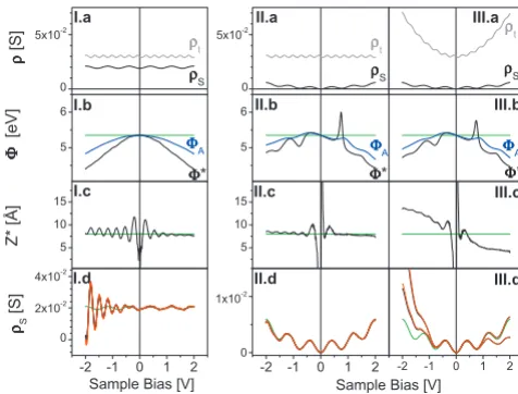
V. EXPERIMENTAL RESULTS
We now present two examples of variable-height scanning tunneling spectroscopy and LDOS recovery on metal and semiconductor surfaces mounted on a dual sample holder that allows measurements with the same tip without the need for sample exchange.
A. Polycrystalline Pt surface
The first experimental example is on polycrystalline Pt layer evaporated on a Ta foil 关see Fig.1共b兲兴. A tungsten tip was inked14with Pt after which spectroscopic measurements
were performed on a nonmodified area of the Pt surface. All experimental data on the metal surface are presented as solid lines in Fig. 4. Figures 4共a兲and4共b兲contain tunneling cur-rents and their bias derivatives taken with set pointz0at 100
pA and 2 V. ⌬z共V兲 was programmed to be constant 0.3 Å while variable⌬z1共V兲and⌬z2共V兲were applied and are
plot-ted in the top part of panel 共a兲in Fig.4 with black and red curves, respectively. The⌽ⴱ共V兲and⌽A共V兲spectra were then obtained from the data in Figs4共a兲and4共b兲and are shown in Fig. 4共c兲. The ⌽A共V兲 spectrum diverges significantly
ap-proaching zero bias corresponding to the fact that I共z2兲
reaches the experimental detection limit and becomes zero at higher bias values thenI共z1兲. In contrast⌽ⴱ共V兲saturates at a
specific value atV= 0 and was used to determine the tunnel-ing barrier⌽= 5.35 eV. This value is reasonable for a Pt tip and Pt sample. Using this barrier value in Eq.共11兲we calcu-lated the zⴱ共V兲 spectrum 关see Fig. 4共d兲兴. The spectrum is strongly corrugated preventing any application of a low-order polynomial fit for thez0 extrapolation atV= 0. Thezⴱ
results also indicate that this particular probe has DOS which is not featureless. We overcome this obstacle by applying the ⌬R1,2 method as in Fig. 2共e兲. The resulting ⌬R1,2 共0.5 V兲 map is plotted in Fig. 4共f兲 showing a local minimum at z0
= 8 Å and⌽= 5.35 eV which supports the⌽ⴱresult in Fig.
4共c兲. The product R1,2共V兲=S,t共V,z1兲/S,t共V,z2兲for z0= 8 Å
and ⌽= 5.35 eV is plotted in Fig. 4共e兲 and is close to the expected value of 1 关from Eq. 共9兲兴 over most of the bias range. The latter gives us confidence that the estimated pa-rameters⌽andz0 are reasonably close to the actual values.
Additionally, these parameters applied in Eq. 共8兲 lead to a very good overlap of the recoveredS,t共z1兲andS,t共z2兲 spec-tra which can be seen in Fig.4共g兲plotted with black and red solid curves. The supplemental material16contains an
analy-sis ofI共z兲measurement that independently confirm the abso-lute separation and estimated barrier height.
B. Si(100)-(4Ã2) surface
and 2 V. The variable-height spectroscopy was performed with constant ⌬z= 0.5 Å and the programmed ⌬z1共V兲 and
⌬z2共V兲are shown on the top of panel共a兲in Fig. 5, as black
and red traces, respectively. Note that for both cases the tip approaches and retracts from the surface in a controlled man-ner as the bias is swept through the band-gap region. The simultaneously measured tunneling currents and their deriva-tives over the bias are presented in Figs. 5共a兲 and5共b兲 and show a high signal-to-noise ratio over the entire bias range, which is the significant advantage of the present variable-height spectroscopy over constant-variable-height measurements. The experimental barrier spectra in Fig.5共c兲are very intriguing. Both ⌽ⴱ共V兲 共black line兲 and ⌽A共V兲 共blue line兲 curves are
observed to decrease in the⫾1 V region approaching values below 1 eV atV= 0, such that it is impossible to estimate the actual tunneling barrier height based on these results. This is in striking contrast to the experimental results on the Pt sur-face 关see Fig. 4共c兲兴. Additionally, extreme deviations are present in thezⴱ共V兲spectrum in the same bias region关black solid line in Fig. 5共d兲兴 which exceed significantly the ob-served in Fig.4共d兲deviations due to the probe DOS. In order to clarify the source of these spectral behaviors in Fig.6we plotted the recovered S,t共V兲 data in logarithmic
ordinate-scale together with the variation in the electric field ⌬Efield共V兲 between the z1 and z2 experiments. Values of ⌽ = 4 eV and z0= 9 Å were used in Eq. 共8兲 which were
ob-tained by the⌬R1,2method for bias of 1.75 V, which is well
outside the ⫾1 V region where these large extreme devia-tions are observed关see Fig.5共f兲兴. A bias of 1.75 V was
cho-sen since the experimentalR1,2共V兲curve in Fig.5共e兲is unity above 1.5 V and for which the⌬R1,2共1.75兲map in Fig.5共f兲
reveals a local minimum at ⌽= 4 eV andz0= 9 Å. This ap-proach continues to demonstrate very good consistency, similar to that found in the case of simulated data in Fig.2共e兲
and for the Pt surface in Fig. 4共f兲. The supplemental material16 contains an analysis of I共z兲 measurement that
in-dependently confirm the absolute separation and the anoma-lous apparent barrier height.
Returning to Fig.6, it is immediately evident that there is a lateral shift in the⫾1 V region between the black and red LDOS curves recovered at different heights. It is in this en-ergy range that the Si surface states are located and given the variation in the electric field between the tip and sample in the two experiments we attribute this effect to a Stark shift of these surface states. The observed blueshift between S,t共z2兲—red and S,t共z1兲—black is indicated with blue
ar-rows in Fig. 6. Thus the origin of the strong corrugation in the⫾1 V range observed in the experimental data shown in Figs. 5共c兲–5共e兲 can be assign to this Stark effect, which is expected to be generally important in studies of semiconduc-tor surface. It is also important to emphasize that the pres-ence of strong deviations of the⌽ⴱ,zⴱ, andR1,2spectra in the
⫾1 V range does not prevent one from determining⌽ and z0using the high positive-bias region. The reasonable values of the latter parameters is manifested by the good overlap of the S,t共z1兲andS,t共z2兲curves plotted in the solid black and red lines in Fig. 5共g兲, respectively. This is an illustration of the benefits of having spectral data available over a wide ⫾2 V bias range in one experiment when using variable-height spectroscopy. -1x10⁻¹⁰ 0 1x10⁻¹⁰ 4 5 6
-2 -1 0 1 2
0.8 1.0 1.2
-2 -1 0 1 2 0 1x10⁻¹⁰ 2x10⁻¹⁰ -30 0 30
-2 -1 0 1 2 0 2x10⁻² 4x10⁻² -1 0 C urrent [A] Φ Φ Φ Φ* Φ Φ Φ ΦA ΦΦΦΦ [eV] R1,2
Sample Bias [V]
dI/dV
[S]
Z*
[Å]
Sample Bias [V]
ρρρρ S, t [S 2 ] ∆∆∆∆ Z[ Å ] g) f) e) d) c) b)
a) 5.0 5.5
7 8 9 Φ Φ Φ Φ[eV] Z 0 [Å] 4E-4 1E-3 0.002000 0.004000 0.005000 0.006000 0.007000 0.008000 0.009000 0.01000 0.02000 0.03000 0.04000 0.05000 0.06000 0.07000 0.08000 0.09000 0.1000 0.2000 0.3000 0.4000 High
Low
[image:6.609.52.293.69.231.2]∆∆∆∆R1,2(0.5)
FIG. 4. 共Color兲VH-STS data and recovery scheme products for
polycrystalline Pt surface and Pt-inked tip. The experimental results
are plotted with solid black forz1and red forz2lines. The
corre-sponding modeled data are shown with dashed curves with the same
corresponding colors. The experimental set point z0 is defined by
the current of 100 pA and sample bias of 2 V. Tunneling currents
and their bias derivatives are presented in共a兲and共b兲, respectively.
In 共c兲 ⌽ⴱ共V兲, ⌽A共V兲, and⌽are shown in black, blue, and green,
respectively. The black curves in共d兲are thezⴱ共V兲 spectra and the
green line is thez0estimate from the local minimum in共f兲.⌬R1,2
intensity map at 0.5 V with ⌽ and z0 as variable parameters is
presented in 共f兲. The corresponding R1,2共V兲 spectra for ⌽
= 5.35 eV andz0= 8 Å derived from the minimum in共f兲are
pre-sented in 共e兲. The combined tip and sample LDOSs recovered by
the scheme are shown in共g兲.
-5x10-11 0 5x10-11 1x10⁻¹⁰ 2 4 6
-2 -1 0 1 2 0.5
1.0 1.5
-2 -1 0 1 2 0 5x10-11 1x10⁻¹⁰ 2x10⁻¹⁰ -30 0 30
-2 -1 0 1 2 0 1x10⁻² 2x10⁻² -2 -1 0 1 Current [A] Φ Φ Φ Φ* Φ Φ Φ ΦA ΦΦΦΦ [eV] R1,2
Sample Bias [V]
dI/dV
[S]
Z*
[Å]
Sample Bias [V]
ρρρρ S, t [S 2 ] ∆∆∆∆ Z [Å] g) f) e) d) c) b)
a) 3.6 4.0 4.4
8 9 10 Φ Φ Φ Φ[eV] Z 0 [Å] 0.001500 0.002000 0.002400 0.003700 0.005000 0.006000 0.007000 0.008000 0.009000 0.01000 0.02000 0.03000 0.04000 0.05000 0.06000 0.07000 0.08000 0.09000 0.1000 0.2000 0.3000 0.4000 High
Low
∆∆∆∆R1,2(1.75)
FIG. 5. 共Color兲VH-STS data and recovery scheme products for
a Si共100兲-共4⫻2兲 surface and Pt-inked tip. The experimental set
pointz0is defined by a current of 50 pA and sample bias of 2 V. The
experimental results are plotted with solid black lines forz1and red
lines forz2. All corresponding modeled data are shown with dashed
curves applying the same color coding. Tunneling currents and their
bias derivatives are presented in 共a兲 and 共b兲, respectively. In 共c兲
⌽ⴱ共V兲,⌽
A共V兲, and⌽are shown in black, blue, and green,
respec-tively. The black curves in共d兲arezⴱ共V兲spectra while with green the
z0estimated from the local minimum in共f兲is plotted.⌬R1,2map at
1.75 V with⌽and z0as variable parameters is shown in共f兲. The
corresponding R1,2共V兲 spectra for⌽= 4 eV and z0= 9 Å derived
from the minimum in共f兲are presented in共e兲. The combined tip and
[image:6.609.316.554.72.237.2]VI. MODELING OF EXPERIMENTAL RESULTS AND SURFACE DENSITY OF STATES RECOVERY
In order to obtain some estimate of the tip LDOS we used our observations from the simulation section of this study
共Sec. IV兲 to model S共V兲 and t共V兲 共both of which are Pt metal兲 and to fit the experimental data in Fig. 4. The esti-mated共⌽andz0兲and programmed共⌬z1and⌬z2兲parameters
from experiment were used unchanged. We tried to keep both densities as similar as possible reflecting their common material composition and no attempt was made to reproduce the fine structure in the experimental spectra. The focus was on the overall curve shapes and intensities. As we showed in Fig.3,共IId兲and共IIId兲, the fine structure of the tip LDOS has little or no influence on the recovered semiconductor surface LDOS so we can neglect it for the recovery of semiconductor surface density of states as described later.
The resulting I共V兲 and dI/dV共V兲 spectra obtained from modeled values of S共V兲 and t共V兲 关see later in Fig. 7 the
exact t共V兲兴 for the Pt metal surface experimental data are presented in Fig.4as dashed lines. We achieved satisfactory agreement between the experimental and the modeled spec-tra ofI共V兲,dI/dV共V兲, andS,t共V兲which is demonstrated in
Figs. 4共a兲,4共b兲, and 4共g兲, respectively. For the ⌽ⴱ and ⌽A curves in Fig.4共c兲the agreement is good in the⫾1 V range while the deviation at high biases is due to the slight devia-tion at the same regions for the tunneling currents关see Fig.
4共a兲兴 and consequently in thedI/dV共V兲 results. In Fig.4共d兲
apart form the high negative-bias region there is no agree-ment between the experiagree-ment and the simulated zⴱ spectra. This is a direct result of the fact that we did not include the tip LDOS fine structure in the modeling which has a major role in thezⴱ共V兲behavior as can be seen in the panels共c兲in Fig. 3. Additionally, the zⴱ共V兲 behavior is very sensitive to spectral noise which is always preset in experimental data. Despite the expected disagreement in panel共d兲in Fig.4, the overall agreement between experimental 共solid lines兲 and modeled 共dashed lines兲 spectra in the rest of the results in
Fig. 4 gives us enough confidence that the modeled tip LDOS reflects the general shape and intensity of the Pt-inked probe used in our experiment and is sufficient to be used for the semiconductor case, namely, the Si共100兲 surface pre-sented in the B part of the previous section.
Next we modeled the Si experimental results as in the Pt case. We used the already modeled tip LDOS form the Pt-surface experiment共see Fig.4兲and applied the estimated共⌽ andz0兲and programmed共⌬z1 and⌬z2兲parameters from the
Si-surface experiment. We kept thet共V兲unchanged and
var-ied the S共V兲 features until a good agreement with
experi-mental I共V兲 anddI/dV共V兲 spectra was obtained for bothz1
andz2. The results of the modeling are presented as dashed
curves in all panels in Fig. 5. The main observation is that the strong corrugation in the⫾1 V region of the⌽ⴱ,zⴱ, and R1,2共V兲spectra is removed for the modeled curves. This is a
direct result of the fact that no Stark effect was included in S共V兲between thez1andz2acquired spectra which confirms
our conclusion. The good agreement between the experimen-tal and modeledS,t共V兲in Fig.5共g兲additionally confirms the
reasonable estimate for the tunneling barrier and absolute separation values.
Finally, using the modeled Pt-tip LDOS plotted as dashed grey line in Fig.7共a兲we recovered the Si共100兲surface LDOS which is presented also in Fig.7共a兲with black line forz1and
red curve for z2. The S共V兲 spectra were obtained from the
S,t共V兲/t共−V兲 product for negative and from the
S,t共V兲/t共0兲product for positive sample biases based on the
summary of our simulations at the end of Sec.IV. The filled and emptyⴱsurface states of the Si共100兲-共4⫻2兲 recon-struction of the sample can be identified. The localized char-acter of the state leads to a well-pronounced peak in the negative-bias range at the onset of the valence band while the delocalized character of the ⴱ state is observed as a low-intensity broad band below the conduction band and the strong Si-dimer back-bond共DB兲.
-2 -1 0 1 2
10-5
10-4
10-3
0.01 0.1 1
ρρρρS,
t
[S
2 ]
Sample Bias [V]
5 6 7 8 ∆∆∆∆E
field
[%
[image:7.609.331.538.68.216.2]]
FIG. 6.共Color兲Recovered combined tip and sample LDOS for a
Si共100兲-共4⫻2兲surface with corresponding variation in the electric
field during the VH-STS experiment. The recovered combined tip
and sample LDOS is plotted in logarithmic ordinate共left兲scale and
shown in black forz1and red forz2. The difference in the electric
field between the tip and the surface for the twoz1andz2ramps is
plotted in blue and the corresponding ordinate is on the top right-hand side of the figure. Blue arrows indicated the blueshift of the LDOS curves with the increase in the electric field.
0
1x10⁻¹
2x10⁻¹
b)
a)
ππππ
ππππ* DB
VB CB
ρρρρt,Pt
LDOS
[S]
-2 -1 0 1 2
0 5
Sample Bias [V]
(dI
/dV
)/(
I/
V
[image:7.609.89.257.70.190.2])
FIG. 7. 共Color兲Comparison of surface LDOS recovered by this
scheme with that using共dI/dV兲/共I/V兲 共Ref.2兲normalization. Black
is used to represent the results fromz1data and red fromz2data.共a兲
shows the recovered Si surface LDOS 共solid lines兲 using this
scheme together with the modeled Pt-inked tip LDOS which is
plotted with grey dashed line. In 共b兲 the corresponding
共dI/dV兲/共I/V兲spectra for the Si surface with solid lines and for the
Pt surface with dashed lines are shown. The spectral feature
assign-ment in共a兲 refers to the Si results. Dotted lines indicated the peak
For comparison the normalized conductance
共dI/dV兲/共I/V兲 共Ref.2兲from the VH-STS experiment on the Si 共solid lines兲and the Pt 共dashed curves兲surfaces are pre-sented in Fig. 7共b兲. No separation invariance is observed, namely, there is significant difference in both the intensity and peak positions for data recorded at different probe-sample separations关seez1—black andz2—red spectra in Fig.
7共b兲兴 in contrast with the results of the present recovery scheme in Fig. 7共a兲. Additionally, all the central features of the 共dI/dV兲/共I/V兲 spectra for the Si surface are artificially shifted toward the Si band-gap region. These two examples demonstrate the unreliability of the 共dI/dV兲/共I/V兲 normalization2 for the recovery of the correct LDOS
espe-cially on semiconductor samples.
VII. SUMMARY
We have introduced a variable-height scanning tunneling spectroscopy 共VH-STS兲 which enables high signal-to-noise I共V兲 and dI/dV共V兲 spectra to be acquired over the entire measured bias range. We presented spectroscopic data taken in the ⫾2 V bias range on two surfaces but with appropri-ately programmed⌬z共V兲 there are no limitations on the ac-tual voltage range. We then introduced a LDOS recovery scheme based on the 1D-WKB approximation proposed by Koslowski et al.10 and tested it on experimental data
ob-tained using VH-STS on metal 共Pt兲and semiconductor 共Si兲 surfaces with good results. The scheme generally recovers the combined tip and surface density of states and we intro-duced a method whereby the tip LDOS can be estimated using a probe inking and characterization method, thus al-lowing a determination of the surface LDOS. To implement this scheme certain parameters are required, namely, the
tun-neling barrier height and the absolute tip-surface separation, and we introduced three methods derived from the VH-STS to determine each of these parameters. The⌽ⴱmethod gives accurate values of the barrier height on metal surfaces while on semiconductor samples significant deviation may occur due to Stark shift of the surface states or/and band banding. The zⴱ method for the absolute separation acquisition de-pends strongly on the tip LDOS and is expected to give accurate values only for flat probe density of states which was not the case for the Pt-inked tip used in this study. The ⌬R1,2method using the two recovered products from the VH
spectroscopy for the parameters determination based on find-ing the local minimum in the⌬R1,2topographic map with⌽ andzas variables gives correct values in all cases, and is in addition supported by the approach to contact I共z兲 experi-ments presented in the supplemental material16for the same
probe and surfaces.
In conclusion the LDOS recovery scheme based on the 1D-WKB approximation is a reliable method applicable for all types of probes and surfaces investigated by scanning tunneling spectroscopy. Combined with VH-STS the scheme introduces three complimentary methods for tunneling bar-rier and absolute separation determination. This combination provides a very powerful surface science tool that enable rigorous LDOS information that directly complements the atomic-resolution capabilities of STM. We expect that this approach will find significant applications in wide areas of surface physics and chemistry.
ACKNOWLEDGMENT
This work was supported by Science Foundation Ireland under PI Award Grant No. 06/IN.1/I106.
1G. Binnig, H. Rohrer, Ch. Gerber, and E. Weibel,Appl. Phys.
Lett. 40, 178共1982兲.
2J. A. Stroscio, R. M. Feenstra, and A. P. Fein,Phys. Rev. Lett.
57, 2579共1986兲.
3For example, S. Modesti, H. Gutzmann, J. Wiebe, and R.
Wie-sendanger,Phys. Rev. B 80, 125326共2009兲.
4For example, J. Mysliveček, F. Dvořák, A. Stróżecka, and B.
Voigtländer,Phys. Rev. B 81, 245427共2010兲.
5V. A. Ukraintsev,Phys. Rev. B 53, 11176共1996兲.
6N. Li, M. Zinke-Allmang, and H. Iwasaki, Surf. Sci. 554, 253
共2004兲.
7B. Koslowski, C. Dietrich, A. Tschetschetkin, and P. Ziemann,
Phys. Rev. B 75, 035421共2007兲.
8C. Wagner, R. Franke, and T. Fritz, Phys. Rev. B 75, 235432
共2007兲.
9M. Passoni and C. E. Bottani,Phys. Rev. B 76, 115404共2007兲.
10B. Koslowski, H. Pfeifer, and P. Ziemann, Phys. Rev. B 80,
165419共2009兲.
11M. Passoni, F. Donati, A. L. Bassi, C. S. Casari, and C. E.
Bot-tani,Phys. Rev. B 79, 045404共2009兲.
12M. Ziegler, N. Néel, A. Sperl, J. Kröger, and R. Berndt, Phys.
Rev. B 80, 125402共2009兲.
13For examples, R. M. Feenstra,Surf. Sci. 603, 2841共2009兲; H. J.
W. Zandvliet and A. van Houselt,Annu. Rev. Anal. Chem. 2, 37
共2009兲.
14B. Naydenov, P. Ryan, L. C. Teague, and J. J. Boland,Phys. Rev.
Lett. 97, 098304共2006兲;Nano Lett. 6, 1752共2006兲.
15J. B. Pethica and A. P. Sutton,J. Vac. Sci. Technol. A 6, 2490
共1988兲.
16See supplementary material at http://link.aps.org/supplemental/
10.1103/PhysRevB.82.245411for verification of results from the
article using approach to contact I共z兲 measurements on the Pt