DIGITAL SYSTEMS
FLOPPY DISK SYSTEM REFERENCE MATERIAL
List of Attachments
FDC-l Interface Manual
Shugart Disk Drive Manual
ALTAIR-Compatible Bus Interface
8080 Software Information
- - - . - ---
---"
"'"
DIGITAL SYSTEMS is currently marketing only the FDC-l
floppy disk controller board and Shugart disk drives. We are
providing documentation on the interface we have used to
inter-face the FDC-l to an Altair compatible machine.
We have used
the resulting system to run CP/M, a sophisticated disk
operat-ing system.
While the bus interface to the FDC-l is a relatively
simple cicuit, the total disk system is complex.
Debugging
a hand wired system may be beyond the capabilities of an
inexperienced TTL designer.
)
DIGITAL SYSTEMS
MODEL FDC-I
FLOPPY DISK CONTROLLER
INTERFACE MANUAL
DIGITAL SYSTEMS
754 Carmel Ave
Livermore, California
94550
(415) 443-4078
This manual is PROPRIETARY INFORMATION of DIGITAL SYSTEMS and
is not
to
be
used
or distributed without the express permission of DIGITAL
SYSTEMS.
Copyright
@
1976
DIGITAL SYSTEMS
,..
IN'!'RODUC'l'ION
This manual provides
the
information needed
to
utilize the
DIGITAL
SYSTEMS
Model
FDC-I
floppy disk controller within a data
system. It is intended as a reference for technical personnel
engaged
is the
specification, design, and implementation of a digital system
with flexible disk drive storage devices. Both hardware
and
software
requirements for integrating the FDC-I with memories, processors, disk
drives, and system wide controlling devices are described.
Details of the interior of the FDC-I do not appear
here;
these
are
found
in
the FDC-I Technical Description manual. Aspects of the
controller detailed here include
specification and
timing
for
all
exterior
interface signals, physical layout, power requirements, and
required command sequences generally supplied under
program
control
from a host processor system to the disk controller.
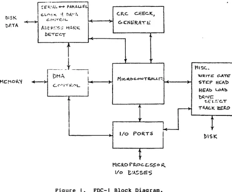
A block diagram of the FDC appears in Figure I.
The FDC-I is a flexible disk drive controller
for
up
to
four
selectable drives.
The
FDC-I uses a high speed microprocessor based
design providing
reliable and
flexible
functions
implemented
in
read-only memory
logic.
Features of the FDC-I include drive write
protect, automatic eRe generation and check, full IBM 3740 compatible
soft sector
formatting,
automatic
track seek verify,
and
head
retraction after eight
idle disk rotations to assure long diskette
life. An automatic bootstrap load from Track 0, Sector I can
be
done
at system initialization without system processor intervention.
The
FDC-I
is fully TTL
implemented
and
compatible.
An
adaptible,
simple
interface to mini
and microprocessor systems is
provided with 8 bit parallel
input and
output busses
for
control
information.
A DMA interface moves data directly in or out of memory
once a transfer is initiated.
Packaging is on
a
single
10"
x
12"
PC
board
with
system
interface via standard edge connectors and flat cable to the flexible
disk drives.
- - - - -
-.
_._--._-_
... ,,- .._
...._-
.. -..._ - - - -
i I
biSK
Df.oTA
I
~e:-;'A!.. ~ PAR~U.f.L.
I
c..Lt"\~~ ~!. t)A'o,,~~
c..';'t;O'0r._'L-bE:TCC"·T
,
(.F.,.c. C.HEC.K,
,.
c;.
CNl:RAT E;.I/o POR.TS
I
HICf;.O F'~oc.c.:.$SO ~
I/o
t,~~SE:5Figure I.
FDC-I Block Diagram.
HARDWARE INTERFACE TO THE FDC-I
t'\\
Soc..,\lJRITG c:.ATtE
STt::P U£:Ab HEAb l.J:)Ab
bC.'vc
!.t~-L. !'"o C. T
I)\SK
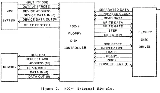
A diagram of the FDC external signals appears in Figure
2.
The
signals can be divided
into three distinct interfaces1 the device,
direct memory
interface
(DMA),
and disk
interfaces.
The device
interface implements command
and
status information between host
system control hardware (i.e. processor and processor support logic)
and
the FDC. The DMA interface exchanges data with up to 64 Kbytes of
random access memory. The disk interface connects the FDC to a
chain
of
flexible disk drives handling
IBM
format compatible diskette
media.
Initialization and
power
supply lines complete
the
FOe
requirements.
A detailed description for each interface follows.
Reference is
made .to the appendices containing backplane signal pinouts
(JI
and
J2), connector pinouts for the disk interface (J3), and the following
table summarizing the mnemonic name, active state, and description
f~all interface signals.
[image:8.613.79.558.44.440.2]r-.
SYSTEM BUSSES
their
8
bits
varies
Following is a summary of the busses and controls for
the
FOC,
names, active state, and description. All busses except MAO are
wide, bit 7 is the most significant bit, bit 0 the LSB. Index x
from
0
to
7
unless otherwise noted.
Name
Active
OINx
hi
-OOUTx
low
MDINx
hi
MDOUTx
hi
-DEVx
low
~tADx
hi
REQ
hi
ACK
hi
-WRITE
low
-IN
low
OUT
high
-IRESE'l'
low
-IOF
low
-BOOTSTRAP
low
DZPROT
high
Description
device input bus
data to host via backplane
device output bus
data from host via backplane
memory data in
data to memory via backplane
memory data out
data from memory via backplane
device address to devices
x ranges from
0
to
15
16
bit memory address bus
to memory via backplane
single line raised by FDC
to request a memory cycle
single line raised by
host memory system to grant
a memory cycle
lowered after cycle is granted
if FDC wishes to write to memory
input device strobe
output device strobe
system restart signal
I/O finished by FOC
forces FDC to execute bootstap
and return -IOF
inhibit writing on disk 0
All bus levels are TTL standard, with low
level
signals below
0.4 VDC and high level signals above 2.5 VDC. All signals listed above
except REQ
and
the last six signals in the table are implemented as
high impedance (TRI-STATE) drivers which may be shared by other
host
system devices using appropriate strobing.
G·aST
iNPUT r,TnOBE
---7
.•.
_---
... - ...--.-
...--OUTPUT STROBE
DEVICE A"DDRESS--
-~
, SEPARATED DATAt
SE P!,-R A.)" ED CLOCK~.QE:
'!
~C ~~D.~ l~~~i.~. (8t~
l
SY'TEM~
READ DATA/ DEVICE OA TA OUT (8)
~--WRITE
DATA...
"
Wr~ITE PROTECT '\. FDC-l WRITE GATE
~
/
---_
...-
-(
s-r.r;e
FFLOPPY
DIRE~TION
~
LOPPY/
DISK DISK
INOP RESET
"-CONTROLLER
"
INOPERATIVE"
D RIVES)
TRACK(- REOUEST ( - - -"'
--
REAllY-_._-REQUEST ACK '\
" iNDEX
"
ADDRESS (16)"
"'
DRIVE SELECT (4)"-MEMORY .... READ/WRITE /
/-...
DATA IN (8)
~.
.._-'" DATA OUT (8)
"
- .
- .
/ '--.
Figure 2.
FDC-I External Signals.
DEVICE INTERFACE
Interaction hetween the host processor or
controlling
hurdwar~and
the
FDC is implementen by the device interface. The controller is
idle until an eight bit address appears
on
the device
andress
bus
(-DEVi)
and
one
oftwo strobes (OUT or
-IN)
appears simultaneously
with the device address. Strobes cause
decoding loqic
to
sense
the
state of
the
-DEVi
bus
and, if it is presenting one of the set
of
addresses given below with the appropriate strobe, a
set of
Dctinns
occurs.
With
a
device address and an OUT strobe, data bits present
on
the device output bus (-DOUTi) will affect the FDC as indicated below.
Device addresses decoded with -IN will cause the FOC to
drive
status
bits onto the device input bus (OINi) for use by the host system. All
signals must
be
stable at
their active level for a minimum of
200
nanoseconds.
l'4ote the loca t ions
0 fthe dev ice add ress
bus
(-DEVi),
dev
ice
input
bus
(DINi),
device output bus (-DOUTi), and strobes OUT and
-IN
on the table in Appendix I.
Device
127D (177Q, 7F
hex)
is
the
status
input
device
when
strobed
by
-IN
and the command output device when strobed by OUT. The
status device delivers eight bits of disk system status to the
device
input
bus bits
0
through
7.
These bits will be stable
100
nanoseconds
after the device address is available and remain stable for as 10n9
~the address and strobe are stable.
1
[image:10.611.60.590.52.360.2]The status bits are:
8it~:
file inoperative - an error signal from the disk indicating
invalid writing sequencing
I:
step ready - indicates 10 milliseconds elapsed since the
last step command was executed and the disk is able to
execute further commands
2:
track zero - indicates that the read/write head on the
selected disk is positioned at the outermost track
3:
I/O finish -
indicates that the FDC has completed
processing (or aborted because of an error condition)
the previous read or write command
4:
track error - indicates the byte read from memory at
the initial
DMAaddress did not match the track byte
of an
10field actually read from the disk. The current
command is aborted.
5:
ID CRC
error - a
CRe
error was encountered in the
10
field of the requested track/sector. Head commands
will com?lete but Write commands are aborteo.
6:
Data CRC error - indicates
a
CRC error in the data fields
during a Read command
7:
Head Unloaded - indicates
at
least eight revolutions of
the disk have occurred since the last Read or Write
command, and the hardware has unloaded the head of the
selected disk.
If
a software error results in a request
for a sector number greater than
260,
this bit and
a zero bit
3 (I/O
never finishes) will iridicate the error
as the FDC will search forever for the requested illegal sector.
When device address
1270
appears with the OUT strobe,
the
bits
on
the device output bus
(-DOUTi)
are
interpreted by the FDC
~scommand bits. The command register in the FDC is loaded using OUT
as a
strobe to the register.
The command bits are:
Bit~:
file inoperative reset - required response to
the file inoperative status bit
I:
step - commands the selected drive to
~ovein the direction
selected by bit 2.
2:
direction - directs the disk drive to step towards
Track
77
(innermost) when active
(-DOUT2
low) and
towards Track
00
when inactive
(-DOUT2
high).
3:
enable - enables loading of drive select bits
4
and
5
4:
drive select - low order of two decoded select bits
5:
drive select - high order of two decoded select bits.
Bits
4
and
5
are latched and decoded to select
one of four drives
as the recipient of all commands
directed to the FOC system. If bit 3 (enable)
is inactive, bits
4
and
5
are ignored in a
command word and the previously selected drive is
used.
6:
Read -
initiate readlng.
~headdress of the memory
buffer has been preloaded into the FOC memory address
register (see below) and the host system has positioned
the selected disk Clt the desired track. The Read command
causes the first byte of the buffer to be fetched and
compared to the track 10 read from the drive. A
mismatch causes a Track error. The second
byte of the buffer
is
fetched and specifies a Sector number
and the FDC reads sector 10 fields until a match occurs.
The third buffer byte is loaded
bythe FOC with the
address mark for the data field read, then 128 bytes
are transferred
from
the drive to memory.
7:
write -
initiates a write operation. Track and sector are
identified as for a Read and a Track error aborts the
operation. After positioning, usinq track
and sector bytes from the memory buffer, the third byte is
written as the address mark for the data field and the
next 128 bytes transferred trom memory to the drive.
Note that all bits, except disk select bits, are
reset on
the
FDe
at
the completion or abort of a Read or
~'Iritecommand.
(\11bits
are cleared when the controller is reset (-IRES8T, below).
Device address 1260
(1760, 7E
hex) is decoded and made available
to the host system on
JI-56as signal -IN126
whenever
it
is
issued
witn
the
-IN
strobe.
It is suggested that the host system use the
signal as a software issued restart command by implementing the
logic
equivalent of
Figure
3.
l\further explanation of Figure
3
appears i r l
the section on initializing the FOC below.
OMA INTERFACE
The DNA interface communicates directly with
any compatible
random
access memory once a Read or Write command is initiated by
the~
host system. This interface uses the OMA address
register
loaded
by
OUT devices
1260
and
1250
as a starting address and always employs
131
sequential
bytes of memory for a disk transfer. When the FOC is ready
to access memory tor any single byte transfer, signal REO
(J2-55)
is
raised.
Nothing
occurs until signal ACK
(J2-56)
appears true, raised
by the host memory system when a memory cycle is granted to
the
FOC.
ACK
should
be raised within
(3e -
memory cycle time) microseconds of
the leading edge of REO in order to service the FOC in time. ACK
must
remain true during the entire memory cycle.
When ACK appears high at the FOC, REO is lowered
and
the
OMA
address
register
is gated to the memory address bus MAOi, and signal
-WRITE is lowered if a memory write (disk read) is requested.
Address
lines are stable within
10e
nanoseconds of the leading edge of ACK. If
-WRITE
remains
high,
a memory read (disk write) is in progress. For
memory read, the host memory must gate the contents of the memory byte
addressed by MAoi onto the memory data out bus MOOUTi (8
bits).
When
the data
is stable, signal ACK must be lowered. The trailing edge of
ACK is used by the FOC
to
latch the data
byte.
Busses
are
then
released by the FOC within 50 nanoseconds of the trailing edge of ACK.
~
If a memory write is requested, the memory address is also gated
to the MAOi bus when ACK appears. In addition, -WRITE is lowered
and
data
to be written in memory is placed on the memory data input bus
MOINi (8 bits). Once
the
host memory
has
captured
the data
and~address, ACK should be lowered and the busses will be released.
The FOC requests
131
sequential bytes of data for each transfer.
The first three bytes are disk address
information:
track number,
sector
number,
and
data
address mark. The remaining
128
bytes are
data. The FOC automatically increments the OMA address
appropriately,
formats data, and generates or checks CRC characters.
In summary, the FOC directly accesses up to 64 Kbytes of
random
access memory using a simple asynchronous handshaking protocol. Memory
address,
READ/WRITE,
input data,
and
output data are used after a
reauest is made and acknowledged indicating that a
memory
cycle
is
granted
to the FOC. Memory buffers of
131
bytes are required for each
transfer.
DISK INTERFACE
The disk interface is a set of signals on
a
separate
50
pin
connector
(J3)
providing
control
and
data paths
to one to four
drives.
A description of each available signal appears below.
All
are
active
low TTL level signals. An asterisk
(*)
next to the signal
name~indicates signals from
the drive
to
the controller.
A plus
(+}1indicates an optional signal not vital to the FOC operation. Refer to
Appendix I for pinout of connector J3.
Device address 1260 when strobed by the OUT
signal
loads the
contents of the -DOUTi data bus into the most significant byte of the
DMA address register. Data on the -DOUTi bus should be stable when the
OUT strobe is issued.
Device address 1250 (175Q, 7D
hex)
when
strobed by
the. OUT
signal
loads the contents of
the -DOUTi
data bus into the least
significant byte of the DMA address register.
In summary,
the device
interface provides
address bits to
activate
the FDC, uses strobes -IN and OUT to synchronize the actions
of the controller with a host system, and has data paths
for
status
and control information. These paths are used by the FDC as follows:
STROBE
ADDRESS
HOST DATA IN
HOST DATA OUT
OUT
1270
none
command word
OUT
1260
none
MSByte DMA address
OUT
1250
none
LSByte DMA address
-IN
1270
status
none
-IN
1260
none
none (JI-56: -INI26)
Name
*+
-FILEINOP
+
-FIR
*
-INDEX
*
-READY
-DS0
-051
-052
-053
-DIR
-STEP
-WRITEOATA
-WG
*
-TRKZRO
*+
-READATA
*
-SO
*
-SC
Description
disk file inoperative - an error
condition from the drive detecting
illegal signal conditions during write
file inoperative reset - response to the
FILEINOP condition from the host system
via the command byte
index pulse indicating rotating diskette
is at the beginning of a track
ready level indicating drive is in an
operable condition(door closed, diskette
up to speed, etc.)
disk select
0 -
disk select lines are
wired one line per drive
disk select
disk select 2
disk select
3
direction - indicates direction head should move
in response to a -STEP pulse. A low (active)
on -DIR indicates stepping toward diskette
center, a high towards diskette edge (Track
0).
step -
10
microsecond pulse to drive when
a head step in the indicated direction is
reauired
interleaved clock and data pulses to be
written onto diskette
write gate - signal windowing WRITEOATA to
enable drive for writing
track zero - active when drive detects
head positioned at track
00
interleaved data and clock pulses from
drive
separated data pulses from drive
separated clock pulses from drive
The FOC requires that the drive electronics provide clock pulses
on the -SC line and data pulses without clocks on
the -SO
line.
-REAOATA
is
unused.
The
-STEP
pulse may
be
longer
than
10
microseconds.
INITIALIZATION
The sample circuitry in Figure 3 illustrates the
initialization
~requirements
for
the Foe. System wide reset circuitry should place a
TTL low signal (-IRESET)
on
JI-55
to
the
FOe
and
preset signal
BOOTSTRAP.
Active
low
-BOOTSTRAP
must
be
available to the Foe on
JI-S7. When the Foe completes its bootstrap procedure of reading track
zero, sector one into OMA
addresses
00-7F
hex,
it will
issue
50
nanosecond
pulse -IOF. In fact, -IOF is issued at the completion of
every disk input or output operation.
-IOF
is used
to
clear
the
BOOTSTRAP latch which in turn may be used to signal the host system to
begin
execution of the bootstrap program now in low memory. BOOTSTRAP
may be invoked under program control by issuing
an
-IN
strobe
with
device
address
1260.
Signal -IN126
will
appear on JI-56 and set
BOOTSTRAP on its trailing edge.
POWER SYSTEM
+5 volts De should be
wired
to
pins
1,2,3,
and
4
of
both
connectors JI
and J2. 2.5 amps may be drawn by the FOC. Pins 83, 84,
85, and 86 of both connectors should be
grounded.
All
odd
numbered
pins on connector J3 are grounded.
WRITE PROTECT
The FOC provides write protection for the disk drive selected by
signal -OS0 or all drives(jumper
selectable).
In order
to
allow
writing,
the
OZPROT signal on JI-9 must be grounded (TTL "0") by the
host system.
IOF"
(Jl-
55)
-=-IN126
)(J1-56)
RESET
> >
-(J1-S9)
- . -~-.-
.
-D Q
BOOTSTRAP
(Jl - 57)
c
(t40ST PROCESSOR RESET)
(POWER ON CU':I\R)
Pigure 3.
Initialization Circuitry.
SOFTWARE
The following system software control by the host' CPU
is required when using the FDC-I:
I.
Software must step the head to the desired track
(using STEP and DIRECTION bits of the command byte)
before reading or writing.
2.
The initial DMA address must be loaded (2 bytes)
prior to issuing a READ or WRITE command.
3.
The three bytes in memory starting at the DMA
address must be set to the desired track, sector,
and address mark (for write).
4.
A simple retry scheme should be implemented to
attempt recovery from disk errors.
(For track
error, seek track
0
and then desired track before
retry) .
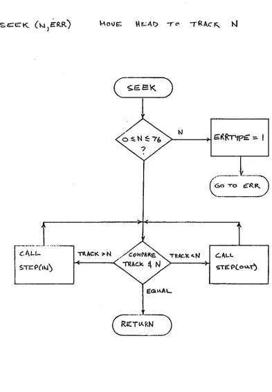
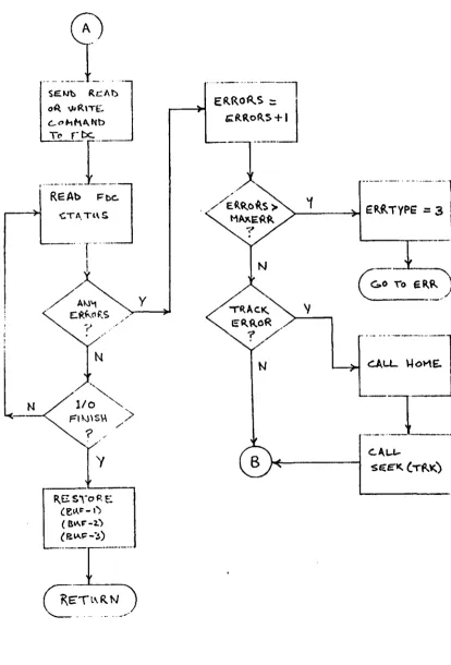
Figures
4
to
7
contain flowcharts for the following routines:
HOME
S'rEP
SEEK
READ
WRI'l'E
seek track zero
step one track in or out
seek any valid track
read one sector
write one sector
Assembly language
code
for
the
above
routines
is
available for
the
8080. Also available is a complete Disk
Operating System for the 8080.
Figure 4.
STEP (}),REC T10N)
SG:!>.)b
DH~. ~
'N
To tllSK
Subroutine HOME.
"
.-
....
-
.._-STE:'P
PULSg
STEP LINE:
Figure 5.
Subroutine STEP.
TRAC.K
-=
0
~E:"l\)b
b\~:: OLtT
oro blSK,
•
>-N _ _
~
G({Rnpt:7::;:.
I
[image:19.611.107.500.79.646.2]I-S_T_C_P_(_IJJ_)_.~
Figure
6.Subroutine
SEEK.RE.Al)
orWRITE
(TR" \
SECT)g\.\F )
ERR..)
SAVE:
(,",~-I)
(E~r~~')
(~"F-3)
Figure 7.
Subroutines READ and WRITE.
[image:20.612.108.503.55.700.2].-.. ---j.
~e.~b ReAl)-.
o~ WR\T£.
c..ot-'lkA,Nb
Tt'
r-
be:.
1I;~
R.ESyoRE
(e~~-'~
( B~~-2.) (P""'j::-~)
, /
>
y
N
-·-····-~~~~l
~CL
::J
Figure 7a.
Subroutines READ and WRITE (cont).
[image:21.612.109.524.65.676.2]APPENDIX I
EDGE CONNECTOR PINOUTS
.J
I
TOP EDGE CONNECTOR
I
+5 VDC
3 +5 VDC
5
7
9II
13
1 5
17 GROUND
19
21 -DEV0 (device address bus)
23 -DEV2
25 -DEV4
27 -DEV6
29 -DOUT0 (data out buss)
31 -DOUT2
33 -DOUT4
35 -DOUT6
37 DIN0 (data in buss)
39 DIN2
41 DIN4
43 DIN6
45 -IN (in strobe)
47
49
51
53
55 -IRESET (initial reset)
57 -BOOTSTRAP
59 -IOF
61
63
65
67
69
71
73
75
77
79
81
83 GROUND
85 GROUND
DIGITAL SYS'l'EMS
2 +5 VDC
4 +5 VDC
6
8
10
12
14
16
18 GROUND
20
22
-DEVI
24 -DEV3
26 -DEV5
28 -DEV7
30 -DOUTI
32 -DOUT3
34 -DOUTs
36 -DOUT7
38 DINt
40
DIN3
42 DINS
44
DIN7
46
OUT (out strobe)
48
Sf!52
54
56 -INt26
58
60
62
64
66
69
70
72
74
76
78
80
82
84 GROUND
86 GROUND
FDC-I Interface Manual
•
J2
BOTTOl"l EDGE CONNECTOR
r'
'"
I
+
5 VDC
2
+
5 VDC
,..,
3
+
5 VDC
4
+
5 VDC
5
6
7
8
9
10
I 1
12
13
14
15
16
17
18
19
20
21 MDIN0
(memory data in)
22 MoINI
23 MDIN2
24 MDIN3
25 MDIN4
26 MDIN5
27 MDIN6
28 MDIN7
29 MAD0
(memory address buss)
30 MADI
31 MAD2
32 MAD3
33 MAD4
34 MAD5
35 MAD6
36 MAD7
37 MAD8
38 MAD9
39 MADI0
40 MAD 1 I
4
I
MADI2
42 MADI3
43 MADI4
44 MADIS
45
46
47 MDOUT0
(memory data out)
48 MDOUTI
49 f4DOUT2
50 MDOUT3
5 1 MDOUT4
52 MDOUT5
53 C"lDOUT6
54 MDOUT7
55 REQ
56 ACK
57
58
59
60
61
62
63
-WRITE
(read)
64
65
66
67 GROUND
68 GROUND
69
70
71
72
73
74
75
76
77
78
79
80
BI
82
83 GROUND
84 GROUND
85 GROUND
86 GROUND
· '
..
J3
DISK DRIVE CONNECTOR
The controller uses a
50
connector cable for communication
with
~
the disk drives. This cable is designated
J3
in the system. Pinout for
the cable is:
PIN
2
4
6
8
10
12
14
16
18
20
22
24
26
28
30
32
34
36
38
40
42
44
46
48
50
SIGNAL NAME
-FILEINOP
-FIR
-INDEX
-READY
(disk file inoperative)
(file inoperative reset)
-DS0
(disk select 0)
-DSI
-DS2
-OS3
-OIR
(direction select)
-S'fEP
-WRITE:DATA
-WG
(write gate)
-TRKZRO
(tr ac k 0)
-REAOATA
-so
(separated data)
-SC
(separated clock)
ALL 000 PINS:
GROUND
---.-DIGITAL SYSTEMS
FDC-I Interface Manual
Page
18
SRBDD/BD~
Diskette Storage Drive
Original Equipment
Manufacturers Manual
TABLE OF CONTENTS
1.0
Introduction
.
.
.
1
1.1
General Description.
1.2
Specification Summary
2
1.2.1
Performance Specifications.
2
1.2.2
Functional Specifications.
2
1.2.3
Physical Specifications.
2
1.2.4
Reliability Specifications.
3
2.0
Functional Characteristics
5
2.1
General Operation
5
,.
r'
2.2
Read/Write and Control Electronics.
6
2.3
Drive Mechanism.
6
2.4
Position ing Mechanism.
6
2.5
ReadlWrite Head.
6
2.6
Recording Format
6
3.0
Functional Operations.
7
3.1
Power Sequencing
7
3.2
Drive Selection.
7
3.3
Track Accessing
7
3.3.1
Step Out.
7
3.3.2
Step In.
9
3.4
Read Operation
9
3.5
Write Operation
.9
TABLE OF CONTENTS Cont.
4.0
Electrical Interface .
· 13
4.1
Signal Interface
· 13
4.1.1
Input Lines .
· 13
4.1.1.1
Input Line Termination
· 15
4.1.1.2
Drive Select 1 - 4 .
· 15
4.1.1.3
Direction Select
· 15
4.1.1.4
Step.
· 15
4.1.1.5
Write Gate
· 15
4.1.1.6
Write Data
· 15
4.1.1.7
Head Load (Optional Input)
· 15
4.1.1.8
In Use (Optional Input)
· 15
1
4.1.2
Output lines
· 16
4.1.2.1
Track Zero
· 16
4.1.2.2
Index
· 16
4.1.2.3
Sector (SA801 Only)
· 16
4.1.2.4
Ready.
· 17
4.1.2.5
Read Data
· 17
4.1.2.6
Sep Data.
· 17
4.1.2.7
Sep Data.
.17
4.1.2.8
Write Protect (Optional)
· 17
4.1.3
Alternate I/O Pins
· 17
4.2
Power Interface
· 17
4.2.1
AC Power.
· 17
1
~
4.2.2
DC Power.
· 18
r
TABLE OF CONTENTS Cont.
5.0
6.0
7.0
Physical Interface.
19
5.1
Jl/Pl Connector.
19
5.2
J5/P5 Connector .
20
5.3
J4/P4 Connector.
20
Drive Physical Specifications
21
6.1
Drive Dimensions.
21
6.2
Mounting Recommendations
21
6.2.1
Vertical Mounting
21
6.2.2
Horizontal Mounting
21
6.2.3
Upright Mounting
23
6.3
Chassis Slide.
23
6.4
Decorative Face Plate
23
Customer I nstallable Options
25
7.1
Drive Select - One to Eight Drives.
27
7.2
Select Drive Without Loading Head
or Enabling Stepper Motor . . .
. . . 28
7.3
Select Drive and Enable Stepper
Without Loading Head. . . .
. . . 29
7.4
7.5
7.6
7.7
7.8
7.9
Load Head Without Selecting Drive
or Enabling Stepper.
Radial Ready . . .
Radial Index/Sector.
Eight, 16, or 32 Sectors
In Use Optional Input (Activity LED) .
Write Protect Optional Use .
iii
29
30
31
32
TABLE OF CONTENTS Cont.
8.0 Operation Procedures . 35
B.l Diskette Loading and Handling 35
8.2
SA 1 0 1 Write Protect 368.3 SA 100 Write Protect 36
9.0 Error Detection and Correction 37
9.1 Write Error 37
9.2 Read Error 37
~
LISTOF ILLUSTRATIONS
1.
SA800/801 Diskette Storage Drive vi2. SA800/BOl Functional Diagram
5
3. Track Access Timing 8
4.
Read Initiate Timing 85. Read Signal Timing . 9
6. Write Initiate Timing 10
7.
Write Data Timing10
8. General Control and Data Timing Requirements.
11
9.
I nterface Connections .14
10.
Interface Signal Driver/Receiver 16~
11.
Index Timing 1612. Sector Timing 16
LIST OF ILLUSTRATIONS Cont.
13. Jl Connector Dimensions 19
14. J5 Connector 20
15. J4 Connector 20
16. Interface Connectors - Physical Location Diagram. 20
17.
Head Load Actuator - Mounting Prerequ isites 2118. SA800/801 Diskette Storage Drive Dimensions . 22
19. Slide Mounting Dimensions. .23
20. SA800/801 PCB Component Locations 26
21. Drive Select Circuitry . 27
22. Select Drive Without Loading Head Circuit. 28
23. Stepper Motor Enable Circuit. 29
24. Load Head Without Selecting Drive
or Enabling Stepper Circuit. 30
25. Radial Ready Circuit 31
26. Radial Index/Sector Circuit. 31
27. Sector Timing Relationships 32
28. Sector Divide Circuit 32
29. In Use/Activity LED Circuit 33
30. Write Protect Circuit 33
31. Loading SA800/801 . 35
32. Diskette Write Protected . 36
33. Write Protect Hole Specifications. . 36
r
Figure 1. SA800/801 Diskette Storage Drive
vi
1
[image:32.612.76.472.166.533.2]1
1.0 INTRODUCTION 1.1 General Description
The SA800/801 are enhanced versions of the successful SA900/901 Diskette Storage Drive. The SA800/801 provides the customer with a mature and reliable product, manufactured to the same high standard of excellence as the 900/90 I. b,·· with additional features.
The SA800 Diskette Storage Drive can read and write diskettes for interchange with other SA800's. the SA900,IBM 3741, 3742 or 3540 and with the new IBM System 32.
The SA80 I provides the same features as the SA800 with additional flexibility for those require· ments which preclude IBM compatibility.
The SA800/801 Diskette Storage Drives have as standard features: a patented diskette clamping! registration design which eliminates the possibility of damage to the diskette due to misregistration and guarantees over 30,000 interchanges with each diskette; single and double density capability on the same drive for the same price; a proprietary ceramic R/W head designed and manufactured by Shugart Associates to provide media life exceeding 3.5 million passes/track and head life exceeding
15,000 hours; an activity light which indicatef drive in use; and ribbon cable or twisted pair ,,\In· nector for ease of packaging. All of these featnes and more are available with the SA800/80 I. SA800/801 Diskette Storage Drives provide the system designer solutions to his applications requirements with greater performance and reliability than cassette or cartridge drives. and lower cost with increased function over card I/O and reel·to·reel tape drives.
Applications for the SA800/801 Diskette Storage Drive are key entry systems, point of sale record· ing systems, batch terminal data storage, micro-program load and error logging, minicomputer program and auxiliary data storage, word process· ing systems and data storage for small business systems.
1.2 Specification Summary
1..2.1 Performance Specifications
Capacity Unformatted
I)er Disk Per Track IBM Format Per Disk Per Track Transfer Rate Latency (average) Access Time
Track to Track Average Settling Time Head Load Time
1.2.2 Functional Specifications
Rotational Speed Recording Density
(inside I rack) flux Density Track Density Tracks Physical Sectors SA800 SABOl Index Encoding Method Media Requirements
SASOO SASOI
1.2.3 Physical Specifications Environmental Limits
Ambient Temperature Relative Humidity Maximum Wet Bulb AC Power Requirements
50/60 Hz ± 0.5 Hz
Single Density 3.2 megabits 41.7 kilobits
2.0 megabits 26.6 kilobits 250 kilobits/sec 83 ms \Oms 260 ms 8 ms ]5 illS
Single Density 360 rpm 3200 bpi 6400fei 48 tpi 77
0 32/16/8
I FM
SA 100/1 BM Diskette SAlOl
= 50°F to 100°F
=
20% to SO%= 7SoF
Double Density 6.4 megabits 83.4 kilobits nla
n/a
500 kilobits/sec 83 ms 10ms 260ms 8 ms 35 msDouble Density 360 rpm 6400 bpi 6400 fei
48 tpi 77
0 32/16/8
I
M2FM
SA 100/IBM Disketre SAlOl
100/ I 15 V AC Installations = 90 to 127 V Co .4A typical :!OO/230 VAC Installations = 180 to 253 V (a .2A typical IX' Voltagc Requircments
+24 VIX' ± 5% 1.3A typical
+ 5 VJX' ! 5% O.XA typical
- 5 VOC ! 5% .OSA typical (option -7 to -16 VOC) Mechanical Dimensions
Width = 45/8 in. Height = I) 1/2 in.
Depth 14 1/4 in. Weight = 13.0Ibs.
Heat Dissipation = 245 BTU/hr. typical
~
1.2.4 Reliability Specifications
MTBF:
PM:
MTTR:
Component Life: Error Rates:
Soft Read Errors: Hard Read Errors: Seek Errors: Media Life:
Passes per Track Insertions:
3
5000 POH under heavy usage 8000 POH under typical usage. Every 5000 POH under heavy usage. Every 15,000 POH under typical usage. 30 minutes.
15.000POH.
I per 109 bils read.
I per 10 12 bits read.
I per 106 seeks.
!
j
;
i
!.~
IH AU II:.::.
--
. . •c", I' 111\ I r.
4 - - - _ .
·~t "<'1 tilt"
4 - - - -
-flRIVt '>I.UC'
.. ,milt 1,,\ f.\
Willi I '''\ 'I
-~!.'.:.
llltH. IIIIN'>1 l ELI
-ORiV~·L$'tlW~l~;-tUACfo:. un
•
.. INnE x • REAll'HtA() tOe.u. WRoTf lOGIC CONIROI lOGIC
2.0 FUNCTIONAL CHARACTERISTICS
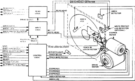
2.1 General Operation
The SA800/80l Diskette Storage Drive consists of read/write and control electronics, drive mechanism, read/write head, track positioning mechanism. and the removable diskette. These components perform the following functions:
Interpret and generate control signals. Move read/write head to the selected track. Read and write data.
The relationship and interface signals for the internal functions of the SA800/80 I are stlOwn . in Figure 2.
The Head Positioning Actuator positions the readl write head to the desired track on the diskette. The Head Load Actuator loads the diskette against
the read/write head and data may then be recorded or read from the diskette.
WRITE PROTECT LEO
[
_. ______ WRITE PROTECT DE lECTOR.---++---~
RlAU HfAD
WHilE HEAU
--_ .. ----, ---':.~
HEAO LOADSOlENUtO ACTIVt!y lIGltT ~~
TRACK 00 LEO _ _ _ _ _
....:3;;:=:::::::::;/
TRACK 00 Of TECTORIN~
DETECTOR
I
WRITE PROTECT - - - LED"DETECTOR
10PTIONAl! STEPPER MOTOR
I
I---'S:..:I-=.EPc.:.p.:;;[R:.:..e:..:':.-.... _ _ _ _ _ _ _ _ _ _ _ _ _ _ _ _ _ _ _ _ ~
STEPPER ' "
SlEPPER 03, _ _ _ _ . _ _ _ _ INDEX OETECTOR
INDEX LED
Figure 2. SA800/801 Functional Diagram
[image:37.611.152.590.418.682.2]2.2 ReadlWrite and Control Electronics TIle clectrunics arc packaged 011 onc PCB. The PCB contains:
I. Index Detector Circuits (Sector/Index for HOI) 2. !lead Position Actuaillf Driver 3. !lead Load Actuator Driver
4. Read/Write Amplilier and Transition Detector 5. Data/Clock Separation Circ:lits
O. Write Proted
7. Drive Ready Deteclor Cin:uit 8. Dnve Seleci Circuits
2.3 Drive Medlanism
The Diskelle drive motor rutate~ the spindle at 360 rpm through a belt-drive system. SO or 60 liz
power is accommodated by challglllg the drive pulIey and belt. A registration hub. centered on the fal:e of the spindle. positions Ihe \)iskelle. A clamp that III lives in I:onjunction wllh the cartridge
guide fixes the lJiskelle to the registration hub. 2.4 Positioning Mechanism
An electrical stepping motor (llead Position Acltllltor) amI lead screw positions the rcad/write head. The stepping motor rotates the lead screw ci'lckwise or counterclockwise in 15" increments. A 150 rotation of the lead screw lIloves the read/ write head one track position. The lIsing system increments the steppmg motor to the desired track. 2.5 ReadlWrite Head
The SAXOO/XU I head is a single element ceramic read/write head with slraddle erase clemen Is 10
provide erased areas between data tracks. Thus normal interchange tulerances between media and drives wiil nol degrade the signal til noise ratio and insures Diskelle illterchangeabili ty.
The redd/write head is mOllnted Oil a I:arriage which is located 011 the Head Position Actuator lead screw. The Diskette is held 11\ a plane perpen·
dicular to the rcad/write head by a platen located on the hase casting. This precise re~istr:ltilln
assures pcrfed compliance with the I-cad/write head_ The Diskellc is loaded agaillst the head with a IU:ld pad al-tuated by the head load ~lIlenuid.
The read/write he<ld is in direct cllntal:l with the Diskette. The head surface has bcen designed tll ubtain maximum signal lransfer til and from the magnetic surfal:e of the Diskette with minimum head/Djsket te w~ar.
6
2.6 Recording Format
'Ine formal of thc dala recorded on the disk is totally a function of thc hUlit syslem. and can be designed ar0und the users applicarion III best take advantage of the lotal available bils tha t can be written on anyone track.
For a detailed discussion of various recording formals. the systems designer should read one of the following:
I. IBM Compatibility Manual Publication number SAOOO6·5
.'!. Shugart Associates Double Density Design Guide Publication number SA0008-0
7
3.0 FUNCTIONAL OPERATIONS
3.1 Power Sequencing
Applying AC and DC power to the SA800/80 I can be done in any sequence, however, once AC power has been applied, a 2 second delay must be introduced before any Read or Write operation is attempted. This delay is for stabilization of the Diskette rotational speed. Also, after application of DC power, a 90 millisecond delay must be introduced before a Read, Write, or Seek operation or before the control output signals are valid. After powering on, initial position of the R/W head with respect to data tracks is indeterminant. In order to assure proper positioning of the R/W head prior to any read/write operation after powering on, a Step Out operation should be performed until the Track 00 indicator becomes active.
3.2 Drive Selection
Drive selection occurs when a drive's Drive Select line is activated. Only the drive with this line active will respond to input lines or gate output lines. Under normal operation, the Drive Select line will load the R/W head, apply power to the stepper motor, enable the input lines and activate the output lines. Optional modes of operation are available to the user by cutting or connecting traces. Reference section 7 for these user install-able features.
3.3 Track Accessing
Seeking the R/W head from one track to another is accomplished by:
a. Activating Drive Select line.
b. Selecting desired direction utilizing Direction Select line.
c. Write Gate being inactive. d. Pulsing the Step line.
Multiple track accessing is accomplished by repeated pulsing of the Step line until the desired track has been reached. Each pulse on the Step line will cause the R/W head to move one track either in or out depending on the Direction Select line. Head movement is initiated on the trailing edge of the Step Pulse.
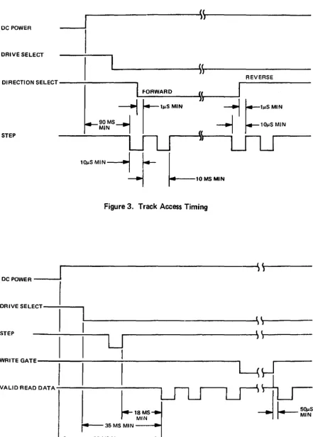
3.3.1 Step Out
~---~~~r---DC POWER
DRIVE SELECT
~~
REVERSE
FORWARD
S~
I
~
~"'MIN
10/JS MIN DIRECTION S E L E C T - - - : - - - . . ,
STEP
Figure 3. Track Access Timing
~---~S\~---DC POWER - - - -...
DRIVE SELECT-~----..,
( l
~---~I~)---STEP
~---~\(~j---U
WRITEGATE---~---~I---~
VALID A EAD DATA - : - - - ,
~~MSt'-~I~-S
....
~---90MSMIN·----~~
·2 SECONDS IF AC AND DC POWER ARE APPLIED AT SAME TIME
Figure 4. Read Initiate Timing
[image:40.617.54.492.61.331.2] [image:40.617.54.495.63.680.2]3.3.2 Step In
With the Direction Select iine at a minus logic level (OV to .4V), a pulse on the Step line will cause the R/W head to move one track closer to the center of the disk. The pulse(s) applied to the Step line must have the timing characteristics shown in Figure 3.
3.4 Read Operation
Reading data from the SASOO/80 I Diskette Storage drive is accomplished by:
a. Activating Drive Select line. b. Write Gate being inactive.
The timing relationships required to initiate a read sequence are shown in Figure 4. These timing specifications are required in order to guarantee that the R/W head position has stabilized prior to reading.
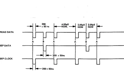
[image:41.613.159.593.400.650.2]The timing of the read signals, Read Data, Sepa-rated Data, and SepaSepa-rated Clock are shown in Figure 5.
READ DATA
I
A B SEP DATA
II
lJ
I
~
~200:!:50ns
----.iU
U
---I
I.--
200 :t SOns SEPCLOCK3.5 Write Operation
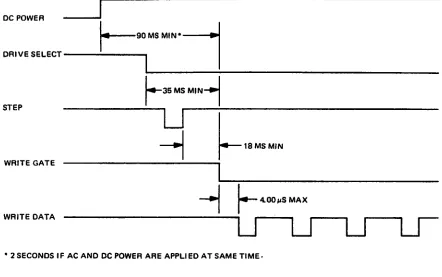
Writing data to the SA800/801 is accomplished by: a. Activating the Drive Select line.
b. Activating the Write Gate line.
c. Pulsing the Write Data line with the data tQ be written.
The timing relationships required to initiate a write data sequence are shown in Figure 6. These timing specifications are required in order to guarantee that the R/W head position has stabilized prior to writing.
The timing specifications for the Write Data pulses are shown in Figure 7.
3.6 Sequence of Events
The timing diagram shown in Figure 8 shows the necessary sequenc'e of events with associated tim-ing restrictions for proper operation.
A
u
B Iu
Au
A = LEADING EDGE OF BIT MAYBE:t 400 ns FROM ITS NOMINAL POSITION. B
=
LEADING EDGE OF BIT MAYBE:t 200 ns FROM ITS NOMINAL POSITION.Figure 5. Read Signal Timing
DC POWER
DRIVE SELECT
r--90 MS M1N0---..j
1
I
STEP
WRITE GATE
WRITE DATA
r-
35 MS MIN-1-~U
I
---1
r--
18 MS MIN---.1
---1~~r_---~--OO-~-S-M-A--X--- ---1~~r_---~--OO-~-S-M-A--X--- ---1~~r_---~--OO-~-S-M-A--X--- ---1~~r_---~--OO-~-S-M-A--X--- ---1~~r_---~--OO-~-S-M-A--X--- ---1~~r_---~--OO-~-S-M-A--X--- U ·
U
u
• 2 SECONDS IF AC AND DC POWER ARE APPLIED AT SAME TIME.
Figure 6. Write Initiate Timing
WRITE DATA C D C C D C
U"'---'U"'---'U
U
U~-U-~ U~-U-~
150n5 MIN \ . -4.00~s
t 20n5--+-
2.0OpS...j1100n5 MAX :t 10ns
Figure 7. Write Data Timing
[image:42.611.44.486.83.360.2]At: POWER
DC l'OWnl
VALID CllNTll0l
OUTI'LIT SIGNALS
DRIVE S~lECl
_____________________ ~' LL ____________________
_'l(~---~. 1T 1 r
j.-~~~~
~---~~l~j---~\l~j---
---I
I-
!JO MS MI NI
~---~~I~J---'\\~---,-1
r-· .. ·
IL-____________________
~\I~I---~\I~I---FORWARD
'H_E_V_E_R_S[~
____~I
\~'.~---~I'\'rl---DIRECTION SH (eT
I
-..f
I----'~, MIN--l
1---
I,,, MINSTEP
WRITE DA I A
WHITf •• AII
VALID HfAU
UATA SIGNAL
.. .J
I--
10., MIN ~I---
lib., MIN_ ___________ I ~ _________________ ~. •
LfLJ
i'lJLJ
) j-1
1--::.:"
I
,,~"'.--!
--11--... ,.,.
H---!--,,",",··\y
~ I~I
I
I.-
NOH 1 - - - + 1I
~
r-".,I",.
~
~W"'""
I
t-NOHI~\J
~~
~!JlJMSMIN'
----I
• 2 SECONDS If AC AND IK POWI H ARE APPLIED AT SAME TIME
NOff- 1 JSlll~ Ill,tl,ml.l0l (1,.1.)" m"OiI t,.. Il1f,oduc .. d .t".·' Dr,,,,@Sf'I"(.1 t()aIIO ...
to' pIO~W'1 'uiOat1luiuf ... ·u.,"q It ~1"lIlt'" ,)rlWP"S to tw dJJlJ11U'd lodP,ltl"ldf>nl u' "p,ll' LndU. UWI • .t1l Rltl\ m .... mum c1P1.1V tnU\' ~ Inuooucpd 10all()l,l\j'
' .. H .. rl·')~"·' ,fltUlln\. Sf'" \Pt"UHl 1 (lit uptHH'al .uUonu'r I "Ua.lldbllf" fp.th"P\
Figure 8. General Control and Data Timing Requirements
[image:43.613.142.591.61.445.2]13
4.0 ELECTRICAL INTERFACE
TIle in terface of the SA800/80 I Disket te drive .;an be divided into two categories:
1. Signal
~. Power
The following sections provide the electrkal delllll' lion for each line.
Reference Figure 9 for all interface connections.
4.1 Signal Interface
TIle signal interface consists of two categories:
I. Control
2.
Data transferAll tines in the signal interface are digital in nature and either provide signals to the drive (input). or
provide signals to the host (output), via interface connector PI/J I.
4.1.1 Input Lines
There are ten (10) signal input lines, eight (S) are standard and two (2) are user installable options (reference section 7).
TIle input signals are of two types. those intended to be multiplexed in a multiple drive system and those which will perform the multiplexing. The input signals to be multiplexed are:
I. Direction Select 2. Step
3. Write Data
4. Write Gate
The input signals which are intended to do t'le multiplexing are:
I. Drive Select I
2. Drive Select 2 3. Drive Select 3 4. Drive Select 4
The input lines have the following electrical specifications. Reference Figure 10 for the recom· mended circuit.
Trlle = Logical zero = Vin ±O.OV to +O.4V
(Ill lin
=
40 ma (max)False = Logical one
=
Yin +2.SV to +S.2SV(a' lin = 0 rna (open)
HOST SYSTEM
---L
-DCGND A7&7loFLAT RIBBON OR TWISTED PAIR
MAX 10 FEET
INDEX
READY
SECTOR 1801 ONLYI
DRIVE SELECT 1
DRIVE SELECT 2
DRIVE SELECT 3
DRIVE SELECT 4
DIRECTION SELECT
STEP
WRITE DATA
WRITE GATE
TRACK 00
WRITE PROTECT (OPTIONALI
READ DATA
SEP DATA
SEP CLOCK
.... +5 VDC
I
,... -5 VDC (-7 to -16 VDCI
l
-
....
+24 VDCX
+24 V RETURNACINPUT FRAME GROUND ACINPUT TWISTED PAIR
·
·
·
-
--SABOO/801 Jl20 19
22 21
24 23
26 25
28 27
30 29
32 31
34 33
36 35
38 37
40 39
42 41
44 43
46 45
48 47
50 49
J5
5 6
4 3
~
-1 2
J4 1 2
n1n
3 FRAME GNDNOTE; Not shown are the nine Alternate I/O connections. The connections for these lines are on pins 2, 4, 6, 8, 10, 12,
14,16, and
la
Signal return for these lines are on pins 1. J. 5. 7,9. 11. 13, IS, 17, and 19 respectivelV. Reference section 7 for uses of these lines.Figure 9. Interface Connections
[image:46.611.52.483.78.678.2]4.1.1.1 Input Line Termination
The SAXOO/XO I has been provided with Ihe capa-bility of terminating the film IIlPllt lines. whkh are meant tu be multiplexed. by jumpering traces. The four lines and their respectivejumpering traces arl!:
I. Dilection Sell!cl . . . Trace "T3" 2. Step . . . Trace "T4" 3. Write l>ata
4. Write Gate
. . . Trace ''15''
. . . Tracc "T6" In order for the drive III function properly, the last dl iw Oil the in terfa!:e must have these four
lines terminated. Termination of these four lines can be accomplished by either 1)1' two methods.
I. Install jumpers (on the last drive) across the posts provided on 'he PCB. The jumpers may be IllstaJled by suldc!rIllg. wirl! wrapping, or by usc of a shorting plug Shugart PIN 15648 or AMI' PIN 530153·2. The shorling plugs arl! not supplied with each Jriw unless it is specified on the order.
2. ExternaJ terminati(lJI Illay be used provided the lerrnlllator is beyond the last drive. Each of the four lines shlluld be terminated by using a 150 (lhm. 14 wall resistor, pulled up tu +5 VOf.
4.1.1.2 Drive Select 1 - 4
Drive Selel.·t when activated to a logical zero level, activates the IllUIt iplexed I/O lines and loads the R/W head. In this Illude of operation only the drive with this line active will respond to the input lines illld gate the uutplll lines.
Four ~eparate input lines. Drive Select I, Drive Select 2, Drive Select J. and Drive Select 4. are provided so that up til fOllr drives may be multi· plexed togethel In a sysklll and have separate Drive Select lilies. Traces 'DS I'. 'DS2'. 'OS3', and 'DS4' 1\;I\'c becn proVIded til ~elcct which Drive Select line will at:tivatt' the interface signals for a . unique drive. As shipped frolll the factory, a
shorl-ing plug is installed on 'DS I'. To select another Drive Sele.'l"t line. this plug should he moved 10 the appropriate 'OS' pin. For additional methods of selecting drive'i. see section 7.1.
4.1.1.3 Direction Select
ThiS in tel face line is a l"IlIIlml signal which defines direction of lIlotion the RjW head will lake when the Step lille is pulsed 1\11 open !:ircuit or II)gical one defines the direclion a~ "Ollt" and if a pulse is :Ipplied III the Step line Ihl' R/W head will move away from the cenlel of till' disk ("IHlversely, if this input IS shorted 10 ground or a logical (.ero
IS
level. the direction of motilln is defined ;.IS "111"
and if a pulse is applied to Ihe step line. the R/W head will move towards the center of the disk.
4.1.1.4 Step
This interface line is a cont rol signal which c!U~es
the R/W head to muve with Ihe direction of motion as dcfined by the Direction Select line. The access motion is initialed on each logical/ero to logical line transition, or the trailing edge of the signal pUlse. Any change in Ihe Direction Sele":1 line must be made at least IlJs before the trailing edgc of the Step pulse. Refer to Figure J for Ihese timings.
4.1.1,5 Write Gate
TIle active state of this signal. or logkal zer,). enables Write Data to be written on the diskette. The inaclive statc, or logical one. enables Ihe read d:lta logll" (Separated Data, Separated Clock. and Read Oala) and stepper logic. Refer to Figure 6
for timings.
4.1.1.6 Write Data
This interf:lce line provides the data til be written lin the diskette. Each transition from a logical one level to a logical zero level. will cause.' the current through Ihe R/W head to be reversed thereby writing a data bit. This line is enabled by Write Gale being active. Refer to Figure 7 for timings.
4.1.1.7 Head Load (Optional input trace 'C')
lllis clIstomer installable option. when activated to ,I logicallcro level and the diskette access d(1(11
is dosed, will load the R/W head load pad against th.: diskette. Refer to section 7 for lIseS and melhod of installation.
4.1.1.8 In Use (Optional input trace '0')