Design and Development of a High-Density, High-Speed
10 kV SiC MOSFET Module
Christina DiMarino
1, Dushan Boroyevich
1, Rolando Burgos
1, Mark Johnson
2, G-Q. Lu
1 1Center for Power Electronics Systems (CPES), Virginia Tech
Blacksburg, VA, USA
E-Mail: [email protected]
2University of Nottingham
Nottingham, UK
Acknowledgements
The authors acknowledge experimental assistance from Meiyu Wang, Yansong Tan, Shan Gao, Yue Xu, Bassem Mouawad, Jianfeng Li, and Robert Skuriat. The donation of substrates from DOWA, and financial support from the Engineering and Physical Sciences Research Council (EPSRC), Rolls-Royce, and the CPES High Density Integration Consortium are greatly appreciated.
Keywords
«Silicon Carbide (SiC)», «Packaging», «High power density systems», «High voltage power converters», «MOSFET».
Abstract
High-density packaging of fast-switching power semiconductors typically requires low parasitic inductance, high heat extraction, and high thermo-mechanical reliability. High-density packaging of high-voltage power semiconductors, such as 10 kV SiC MOSFETs, also requires low electric field concentration in order to prevent premature dielectric breakdown. Consequently, in addition to the usual electromagnetic, thermal, and mechanical analyses, the electric fields must also be evaluated. This is the first detailed report on the optimization of a high-voltage SiC MOSFET power module.
Introduction
High-voltage silicon carbide (SiC) transistors have been demonstrated in recent years, and now Wolfspeed’s 3rd-generation 10 kV, 350 mΩ SiC MOSFET [1] is becoming available. This device is capable of switching higher voltages faster, and with lower losses, than silicon (Si) IGBTs [1]. These features reduce the complexity of medium-voltage systems since simpler topologies with fewer levels can be used, and allow for the realization of new applications.
The 1st-generation 10 kV SiC MOSFETs were packaged in a module that was based on a standard 140 mm × 190 mm footprint typically used for slower, lower-voltage Si IGBTs [2],[3]. Given the
improved performance of the 3rd-generation 10 kV SiC MOSFETs [1], new packaging technologies are needed in order to realize their full potential. One notable difference between the two devices is that the 1st-generation SiC MOSFET degraded during body diode conduction [4]. Consequently, in the first 10 kV, 120 A power module, antiparallel 10 kV SiC junction barrier Schottky (JBS) diodes were used to conduct reverse current [3]. Further, in order to ensure that the body diode did not conduct before the JBS diode, low-voltage Si Schottky diodes were placed in series with the SiC MOSFETs [3]. However, the 3rd-generation SiC MOSFET does not suffer from this type of degradation, and can therefore be safely operated in the third quadrant [5].
MOSFET/JBS diode module [2],[3]. However, the power density of this latest 10 kV module (approximately 4.2 W/mm3 [6]) can still be improved.
The aim of this work is to develop a high-power-density, high-speed, half-bridge module using Wolfspeed’s 3rd-generation 10 kV SiC MOSFETs without antiparallel diodes; instead, the reverse current will flow through the MOSFET channel, and the body diode will only conduct during the deadtime. Of course, there are several challenges associated with this objective. Most notably, the desire for high density will increase the electric field concentration. This is a new challenge that has not been explicitly addressed before, and it arises from the development of these voltage, high-density SiC die. High-high-density packages also have greater power dissipation densities, thereby requiring a more thoughtful thermal design. Additionally, when operating in synchronous mode, the SiC MOSFETs have higher average power dissipation, hence further emphasizing the need for a package with low thermal resistance and a good thermal management system.
Several challenges are also associated with high-speed switching. In particular, sensitivity to parasitic inductance increases, which can cause significant voltage overshoot and ringing, as well as current imbalance among paralleled die [2]. Furthermore, the high voltage rate of change (dv/dt) can result in common-mode (CM) current flowing through the parasitic capacitance that exists between the die and the cooling system. This paper will address these challenges in order to achieve a density, speed 10 kV SiC MOSFET module. This is the first detailed report on the optimization of a high-voltage SiC MOSFET module package.
Module Design
In this section, the design of a 10 kV, 54 A SiC MOSFET half-bridge module will be presented. The substrate design and die arrangement will first be discussed, followed by the termination design.
Substrate Design and Die Arrangement
Substrates are needed to provide the interconnection of the devices within the power module, as well as the voltage isolation between the module and the cooling system. In this work, direct-bonded aluminum (DBA) is used with 1-mm-thick aluminum nitride (AlN) and 0.3-mm-thick aluminum (Al). DBA was selected because it has higher thermal-cycling capability compared to direct-bonded copper (DBC) substrates [7]. AlN was chosen due to its high thermal conductivity, and because it is available in 1-mm thickness, which provides the necessary voltage isolation.
In order to address the enhanced electric field and thermal effects associated with a voltage, high-density design, the DBA substrate must be carefully designed and evaluated. The ceramic of the DBA typically has a dielectric strength around 20 kV/mm. At 10 kV, one would think that 1-mm-thick AlN would provide sufficient margin such that the module could operate reliably at this high voltage. However, the peak electric field will actually be much greater than the expected 10 kV/mm. This is because the electric field will be highly concentrated at the triple point, which is where the AlN, Al, and encapsulation meet (Fig. 1) [8]. If this electric field exceeds the breakdown field strength of the insulation materials (i.e. the AlN or encapsulation), then partial discharge (PD) can occur. Repetitive PD events can ultimately result in insulation failure, thus destroying the power module [8].
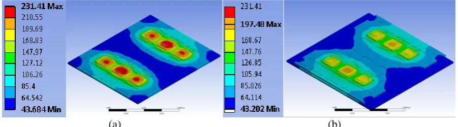
This phenomenon is demonstrated by ANSYS Maxwell 2D electrostatic simulations (Fig. 1). Fig. 1a and Fig. 1b show the electric field distribution for the case when the top and bottom metal layers are symmetrical. For this case, the peak electric fields both within the bulk AlN and at the triple points are reduced by 40 % when two DBA substrates are stacked together (Fig. 1b) compared to when there is only a single DBA substrate (Fig. 1a). This reduction is due to the potential of the middle metal layer, which, due to the vertical symmetry of the stacked substrate structure, floats to half of the voltage applied across the top and bottom metal layers. For example, when 10 kV is applied across the top and bottom metal layers, then, due to the vertical symmetry, the middle metal layer will float to 5 kV.
[image:3.595.72.523.525.650.2]Fig. 1c and Fig. 1d show the electric field distribution for the case when the top metal substrate is patterned and has different potentials. It can be seen that, when the middle metal layer is left floating, the peak electric field is not as notably reduced (Fig. 1c) compared to the case with the vertical symmetry (Fig. 1b). This is because the asymmetry and different potentials cause the middle metal layer to float to a potential that is less than half of the applied voltage (2.4 kV for this example). Accordingly, the reduction in the peak electric field is not as prominent (27 %, compared to 40 %). However, if the middle metal layer is electrically connected to half of the applied voltage (Fig. 1d), then the electric field is again reduced by 40 % compared to the single-substrate case (Fig. 1a).
Fig. 1: Electric field plots from 2D electrostatic ANSYS Maxwell simulations for (a) a single DBA with vertical symmetry and a single potential on the top and bottom Al layers, (b) two stacked DBAs with vertical symmetry and a single potential on the top and bottom Al layers, (c) two stacked DBAs with vertical asymmetry and two different potentials on the top Al layer with the middle metal layer left floating, and (d) two stacked DBAs with vertical asymmetry and two different potentials on the top Al layer with the middle metal layer connected to half of the applied voltage (5 kV).
(a) (b)
Fig. 2: 3D steady-state thermal simulation for (a) a single DBA, and (b) two stacked DBAs. Each die has a heat flow of 200 W. A heat transfer coefficient of 5000 W/m2K is applied to the bottom surface.
increased heat spreading that is provided by the second DBA. Consequently, the baseplate can be eliminated, and direct-substrate cooling can be utilized.
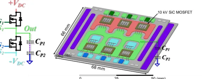
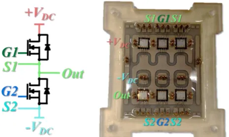
Fig. 3 shows the designed half-bridge power module, which has three 10 kV, 350 mΩ, 8.1 mm × 8.1 mm die in parallel per switch position for a total module current of 54 A. This value is based on the preliminary datasheet for the 10 kV SiC MOSFET die, which rates the continuous drain current at 18 A for a case temperature of 90 °C, junction temperature of 175 °C, and gate-source voltage of 20 V.
As mentioned earlier, the parasitic capacitance between the SiC die and the cooling system is a path for CM current under high-dv/dt switching. Specifically, the parasitic capacitance between the output trace in the top Al layer (“Out”) and the bottom Al layer (connected to the cooling system) are of interest since the output node (i.e. the source of the top switch and drain of the bottom switch) experiences high dv/dt as the top and bottom switches in the half-bridge alternately conduct. By stacking two DBAs, this capacitance is reduced by 20 % since there are now effectively two parasitic capacitors in series. For a single DBA, the parasitic capacitance between the output trace and the bottom Al layer is 80 pF (CP1). When two DBAs are stacked together, the effective capacitance
becomes 64 pF due to the series connection of a 320-pF capacitor across the second DBA substrate (CP2). These values, which were simulated using ANSYS Q3D Extractor, are in good agreement with
the calculated capacitances. Additionally, when the middle metal layer in the DBA stack is connected to the dc bus midpoint (to reduce the peak electric field), then part of the CM current that flows through CP1 will be diverted back to the dc bus rather than going through CP2 to the cooling system.
[image:4.595.135.468.390.521.2]This will hence reduce the amount of CM current that flows through the system ground. The amount of CM current that is diverted will depend on the high-frequency impedance of the connection path between the middle metal layer and the dc bus.
Fig. 3: Designed 10 kV, 54 A half-bridge module with stacked DBAs (DBA1 and DBA2). The color of the Al trace corresponds to the node in the schematic (left) with the same color.
Termination Design
Another challenge associated with the high-density design is the module termination. Specifically, the interfacing of the module with the rest of the high-voltage system is non-trivial since standards stipulate minimum creepage and clearance distances between exposed conductors; creepage is the shortest distance between two conductors along the surface of a solid insulating material, while clearance is the shortest distance between two conductors in air. According to UL-840, the minimum clearance distance for electrical equipment rated at an impulse withstand voltage peak of 12 kV is 14 mm [12]. At 10 kV operating voltage, the minimum creepage distance is 100 mm for material group IIIa,b (e.g. FR4) and pollution degree 2 (normally non-conductive pollution with some temporary conductivity caused by condensation) [12]. Clearly these standards make it difficult to achieve a high-density package for high-voltage semiconductors due to the large distances needed for the connection to the system. However, in this work, a custom design that avoid exposed conductors was developed, so the minimum creepage and clearance distance requirements do not apply.
Several terminal types were considered: 1) busbar, 2) pins, and 3) springs. These designs were evaluated based on the tradeoffs between peak electric field, current-carrying capability, parasitic inductance, ease of assembly, connection method, and reliability. Busbars are common in high-power modules due to their high current-carrying capability and lamination option, which offers lower inductance. However, the sharp edges result in high electric field concentration. Pin and spring
connectors, on the other hand, have a rounded geometry, resulting in lower electric field concentration. Moreover, busbars and pins are through-hole connections and are typically secured using screws, solder, or press-fit sockets. This is undesirable for this work because, in order to avoid the minimum creepage and clearance distance requirements, the conductors must be insulated. This could be done by potting or encapsulating the exposed conductors after connecting the module to the system.
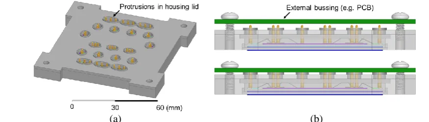
However, this could make the disassembly difficult and impractical. In terms of mechanical reliability and ease of connecting and disconnecting the module, spring connectors are preferred compared to rigid busbars and pins. Multiple springs can also be placed in parallel to reduce the parasitic inductance. Further, the springs can be distributed throughout the module to maintain impedance symmetry for the paralleled die. The scattered terminals also create a more even pressure distribution throughout the module, providing uniform contact to the cooling system. For these reasons, springs were chosen for the module terminals.
The springs selected for this module each have a current rating of 10 A. The arrangement of the spring terminals is shown in Fig. 4. According to ANSYS Q3D Extractor, the gate-loop inductance for each MOSFET die is 9 nH with the spring terminals. This is more than two times lower than the gate-loop inductance reported in [2], which models a package intended for 10 kV SiC MOSFETs. For the power loop, the total parasitic inductance is 9 nH with the spring terminals. This is 76 % lower than the power-loop inductance reported in [2], and 44 % lower than that reported in [6]. Moreover, this improved layout provides more symmetrical impedances for each of the paralleled die compared to those in traditional modules, which, as shown in [2], can have more than 100 % difference in the peak current among the paralleled die during the switching transients.
a higher breakdown field strength. The power density of the designed module is 7.0 W/mm3, which is 67 % greater than that of Wolfspeed’s 3rd-generation 10 kV, 240 A SiC MOSFET module [6].
Fig. 4: Designed 10 kV, 54 A half-bridge module with spring terminals. The color of the Al trace corresponds to the node in the schematic (left) with the same color.
(a) (b)
Fig. 5: (a) 3D model of the module with the housing and lid, and (b) side views of the module showing the external busbar (green) compressing the spring terminals until it contacts the protrusions in the lid.
Module Fabrication
In this section, the fabrication of the 10 kV SiC MOSFET module will be presented. The bonding of the insulating substrates to form the stacked structure will be discussed, followed by the die attach methods and results. The encapsulation process will also be presented in this section.
Substrate Attach
A large-area silver (Ag) sintering process was developed to attach the two DBAs together. Ag sintering was selected because of its low voiding content, high thermal conductivity, and its low processing temperature yet high melting temperature after sintering (960 °C). This last point is significant because the SiC MOSFET die are attached after the DBAs have been bonded together. If solder is used to bond the two DBAs, then the processing temperature of the die attach material must be below the melting temperature of the solder used for the DBA attachment.
The DBAs were plated with Ag by the manufacturer to make them compatible with Ag-sintering. Two separate Ag paste layers (200 µm apiece) were printed on each of the two DBAs with bonding areas of approximately 58.5 mm × 48.5 mm. These layers were dried at 120 °C until all the solvent evaporated. After the drying process, the DBAs were sintered together at 260 °C for 1 hour with 5 MPa of
[image:6.595.78.516.284.409.2]Die Attach
Two die attach methods were evaluated in this work: 1) soldering and 2) pressure-less Ag-sintering. For the soldering, 50-µm-thick 96.5Sn/3.5Ag preform with 1 % NC-10HF flux coating from Indium Corporation was used. This preform was selected because it is compatible with the Ag-plating of the DBAs, and it has a high melting temperature of 221 °C. To test this method, a 10 kV SiC MOSFET die was soldered to a Ag-plated DBA. The soldering was done in air at 260 °C. The die shear tests revealed a bonding strength of 36 MPa; however, the x-ray images showed significant voiding
(approximately 40-50 %). Hence, a high thermal resistance can be expected. Vacuum reflow soldering could be used to reduce the voiding content.
It has been shown that sintered-Ag bonds have lower thermal impedance and better thermal cycling capability than soldered joints [13]. Since it is desirable to have a low package thermal resistance, Ag sintering was evaluated for the die attach. Several of the 8.1 mm × 8.1 mm 10 kV die were cut into 4 mm × 4 mm pieces since they could be sheared off with lower force (< 100 kgf). Each of these pieces were sintered without pressure using different types of Ag paste and sintering profiles. The die sintered with Kyocera’s CT2700R7S Ag paste at 200 °C for 90 minutes had the highest bonding strengths (> 45 MPa). A whole 8.1 mm × 8.1 mm die was then sintered under the same conditions, but the die shear test revealed a bonding strength of only 14.3 MPa. The reason for the lower bonding strength is still being investigated. It should be noted that these 10 kV SiC MOSFET die have gold (Au) metallization on the bottom surface. Since Ag diffuses faster than Au, a sintering profile that limits the Ag diffusion is essential. If too much Ag diffuses into the Au, then Kirkendall voids will form at the Ag-Au interface, resulting in a bond with low shear strength [14]. Applying pressure during sintering can improve the shear strength by creating a denser Ag layer [14]. However, pressure-assisted sintering is a more complex process, especially when sintering multiple die simultaneously since the pressure must be uniformly applied to all of the die.
Encapsulation
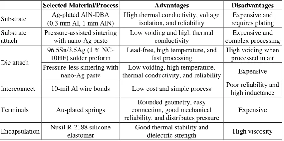
[image:7.595.72.528.533.759.2]Encapsulation protects the die from environmental factors, such as moisture and radiation, and improves the electrical insulation. A study compared seven different encapsulation materials in terms of their processability before curing, the temperature-dependence of their dielectric properties (permittivity and dielectric strength), and the degradation of their dielectric properties after thermal aging at 250 °C [15]. From this study, it was determined that silicone-based materials have low outgassing and superior high-temperature performance [15]. Accordingly, a silicone-based material (NuSil R-2188) was selected for this work. Table 1 lists the materials used for the designed module. Table I: Packaging materials and processes used for the 10 kV SiC MOSFET module
Selected Material/Process Advantages Disadvantages
Substrate Ag-plated AlN-DBA (0.3 mm Al, 1 mm AlN)
High thermal conductivity, voltage isolation, and reliability
Expensive and requires plating Substrate
attach
Pressure-assisted sintering with nano-Ag paste
Low voiding and high thermal conductivity
Expensive and complex processing
Die attach
96.5Sn/3.5Ag (1 % NC-10HF) solder preform
Lead-free, high temperature, and fast processing
High voiding when processed in air Pressure-less sintering with
nano-Ag paste
Low voiding, high temperature,
thermal conductivity, and reliability Expensive Interconnect 10-mil Al wire bonds Low cost and simple process Poor reliability and
high inductance
Terminals Au-plated springs
Rounded geometry, easy connection, good mechanical reliability, and distributes pressure
Expensive
Encapsulation Nusil R-2188 silicone elastomer
Good thermal stability and
The fabricated 10 kV SiC MOSFET module is shown in Fig. 6. This module is made of semi-functional 10 kV SiC MOSFET die. This was done to test the fabrication processes and PD without damaging the fully-functional devices. Once all of the tests have been completed and the processes have been optimized, the module will be constructed using the fully-functional 10 kV die.
Fig. 6: Fabricated prototype module with semi-functional 10 kV SiC MOSFET die.
Module Testing
In this section, the testing of the fabricated 10 kV SiC MOSFET module will be presented. First, the results of the static characterization will be shown, followed by those from the PD testing.
Static Characterization
A Keysight B1505A curve tracer was used for the static characterization. All tests were done at 25 °C. The on-resistances of each MOSFET in the fabricated module are shown in Fig. 7a. As mentioned previously, the die in this module are semi-functional, hence the on-resistances are higher than the typical 350 mΩ (at 15 A) that is specified in the preliminary manufacturer datasheet. However, the on-resistances are still below the specified maximum value of 450 mΩ, and have a mild variation of 7 %. The drain leakage currents for the top and bottom switches in the fabricated half-bridge module are shown in Fig. 7b. The top switch is able to block 10 kV with a leakage current of approximately 7 µA. However, the bottom switch has a breakdown voltage of 7.3 kV. Since these die were selected from a batch of semi-functional devices, it is not unlikely for some of them to have breakdown voltages below 10 kV. Due to equipment limitations, the bare die characterization was performed in air, so the testing voltage was limited to a couple thousand volts. As such, it is unknown if one or more of the die in the bottom switch position had a low breakdown voltage prior to packaging.
(a) (b)
Fig. 7: (a) On-resistance versus drain current for each of the six semi-functional die in the fabricated module at 25 °C and a gate-source voltage of 20 V, and (b) drain current versus drain-source voltage for the top (red) and bottom (blue) switches in the module at 25 °C and a gate-source voltage of 0 V.
Partial Discharge Testing
[image:8.595.183.416.133.272.2]Partial discharge testing setup
[image:9.595.119.477.173.326.2]PD tests were conducted to validate the electrostatic ANSYS Maxwell simulations. The PD tests were performed using a high-frequency current probe (91550-1 from ETS-Lindgren) to measure the PD current, and a high-voltage passive probe (P6015A from Tektronix) to measure the applied voltage. A HiPot tester, with a line-frequency ac output voltage, was used as the excitation source. The tests were performed in air so that the PD signals could be observed at lower excitation voltages. The testing setup is shown in Fig. 8. The testing was done in an EMI chamber to improve the signal-to-noise ratio.
Fig. 8: PD testing setup (left) and testing fixture (right) for the module DBA substrates. Partial discharge testing results
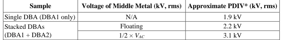
From the testing, it was revealed that, as was shown in the electrostatic simulations, the PD will occur at the triple point. Specifically, the PD will take place along the edge of the Al pad where the high potential is applied. The PD inception voltage (PDIV) for a single DBA substrate is 1.9 kV rms when the sample is tested in air. In the actual power module, the substrate is encapsulated with silicone elastomer, which has a higher breakdown strength than air (19.5 kV/mm compared to 3 kV/mm). Therefore, the PDIV is higher in the encapsulated module.
When two DBAs are stacked together and the middle metal layer is left floating, the PDIV increases by 15 % to 2.2 kV rms. This is due to a slight reduction of the electric field at the triple point since the middle metal layer will float to approximately 0.31 kV rms, which is one-seventh of the applied excitation voltage (2.2 kV rms). This potential was calculated based on the ratio of the series parasitic capacitors across the top and bottom DBAs, which form a capacitive voltage divider. This case was also simulated in ANSYS Maxwell. The simulated potential of the middle metal layer for an applied voltage of 2.2 kV was 0.32 kV, which is 3 % higher than the calculated value.
As mentioned earlier, the potential of the middle metal layer has a significant impact on the electric field (Fig. 1). Accordingly, another PD test was performed on the stacked DBA sample, but this time the middle metal layer was connected to approximately half of the applied excitation voltage. In this case, the PDIV increased to about 3.1 kV rms. This is an increase of 63 % compared to the case with a single DBA substrate. These PD testing results are summarized in Table II. No PD could be detected in the fabricated module up to approximately 4 kV rms. Beyond this voltage, the PD from the HiPot tester and its connectors became too high to identify signals from the module.
Table II: Partial discharge testing summary
Sample Voltage of Middle Metal (kV, rms) Approximate PDIV* (kV, rms)
Single DBA (DBA1 only) N/A 1.9 kV
Stacked DBAs (DBA1 + DBA2)
Floating 2.2 kV
1/2 × VAC 3.1 kV
[image:9.595.66.525.674.740.2]Conclusion
In this work, a 10 kV, 54 A SiC MOSFET half-bridge module was designed and a preliminary prototype was fabricated using semi-functional 10 kV SiC MOSFET die. The gate- and power-loop inductances of the designed module are each 9 nH (including the spring terminals), and the power density is 7.0 W/mm3. These low inductances and high power density were achieved by eliminating the antiparallel diodes and optimizing the substrate design and die and terminal arrangement. The electric fields in the module were also optimized; stacking two DBAs together and connecting the middle metal layer to half of the applied voltage increased the PDIV by 63 %. Due to the patterns and different potentials on the topside of the substrate, if the middle metal layer is left floating, then it may not drift to a potential that will result in a meaningful reduction in the peak electric field. Additionally, connecting the middle metal layer to the dc bus midpoint will reduce the CM current that flows through the system ground since it creates a path for the current to flow back to the dc bus. The static characterization of the fabricated module with semi-functional 10 kV die showed that the top switch in the half-bridge is able to block 10 kV with a leakage current of 7 µA at 25 °C, while the bottom switch has a breakdown voltage of 7.3 kV. No PD could be detected in the fabricated module up to 4 kV rms.
References
[1] V. Pala, E. V. Brunt, L. Cheng, M. O’Loughlin, J. Richmond, A. Burk, S. T. Allen, D. Grider, J. W. Palmour, “10 kV and 15 kV silicon carbide power MOSFETs for next-generation energy conversion and transmission systems,” in IEEEECCE, 2014.
[2] Z. Chen, R. Burgos, D. Boroyevich, F. Wang, S. Leslie, “Modeling and simulation of 2 kV 50 A SiC MOSFET/JBS power modules,” IEEE EPE, 2009.
[3] M. Das, D. Grider, S. Leslie, R. Raju, M. Schutten, A. Hefner, “10 kV SiC power MOSFETs and JBS diodes: enabling revolutionary module and power conversion technologies,” J. Mat. Sci. Forum, vol. 717-720, pp. 1225-1228, 2012.
[4] A. Agarwal, H. Fatima, S. Haney, S. H. Ryu, “A new degradation mechanism in high-voltage SiC power MOSFETs,” IEEE Electron Device Lett., vol. 25, no. 7, pp. 587-589, 2007.
[5] B. Hull, S. Allen, Q. Zhang, D. Gajewski, V. Pala, J. Richmond, S. Ryu, M. O’Loughlin, E. VanBrunt, L. Cheng, A. Burk, J. Casady, D. Grider, J. Palmour, “Reliability and stability of SiC power MOSFETs and next-generation SiC MOSFETs,” in IEEE WiPDA, 2014.
[6] B. Passmore, Z. Cole, B. McGee, M. Wells, J. Stabach, J. Bradshaw, R. Shaw, D. Martin, T. McNutt, E. VanBrunt, B. Hull, D. Grider, “The next generation of high voltage (10 kV) silicon carbide power modules,” in IEEE WiPDA, 2016.
[7] D. P. Hamilton, S. Riches, M. Meisser, L. Mills, P. Mawby, “High temperature thermal cycling performance of DBA, AMB and thick film power module substrates,” in IEEE CIPS, 2016.
[8] J. H. Fabian, S. Hartmann, A. Hamidi, “Partial discharge failure analysis of AlN substrates for IGBT modules,” J. Microelectron. Rel., vol 44, pp. 1425-2430, 2004.
[9] O. Hohlfeld, R. Bayerer, T. Hunger, H. Hartung, “Stacked substrates for high voltage applications,” in IEEE CIPS, 2012.
[10] R. Wu, L. Smirnova, H. Wang, F. Iannuzzo, F. Blaabjerg, “Comprehensive investigation on current imbalance among parallel chips inside MW-scale IGBT power modules,” in IEEE ICPE-ECCE Asia, 2015.
[11] F. Stueckler, E. Vecino, “CoolMOSTM C7 650V switch in a Kelvin source configuration,” Applicat. Note, AN-2013-05, V1.0, 2013.
[12] Standard for Insulation Coordination Including Clearances and Creepage Distances for Electrical Equipment, UL 840, 2007.
[13] X. Cao, T. Wang, K. D. T. Ngo, G. Q. Lu, “Characterization of lead-free solder and sintered nano-silver die-attach layers using thermal impedance,” IEEE Trans. Compon. Packag. Manuf. Technol., vol. 1, no. 4, Apr. 2011.