Comparison of Power Line Filter
Orientations
Wei Wang
M.Sc. Thesis
October 2019
Supervisors:
prof. dr. F.B.J. Leferink (Frank) dr. ir. D.J.G Moonen (Niek) B ten Have M.Sc. (Bas) dr.ir. A.B.J. Kokkeler (Andre) Nemashkalo, D. M.Sc. (Daria)
Telecommunication Engineering Group Faculty of Electrical Engineering, Mathematics and Computer Science University of Twente P.O. Box 217
Abstract – There are nearly no electronic products
nowadays that can comply with the conducted emission regulatory requirements without the use of some form of filter. In this thesis research is performed on an one-stage power line filter, of which was observed that changing the installation orientation, could influence the filter characteristic. Simulations are used to analyze the power line filter itself, and investigate the reason of changing filtering behaviors by different orientations. Furthermore, different measurements are performed with different switched mode power supplies, to verify the simulation results.
1 INTRODUCTION
Electromagnetic interference (EMI) is defined as unwanted electrical signals and can be in the form of conducted or radiated emissions. If the noise travels along electrical conductors, or electronic components, it is conducted EMI. Electrical noise that travels through the air or free space as electro, magnetic or electromagnetic fields is called radiated EMI [1].
Conducted emission regulations are intended to control the emission from the public alternating current (AC) power distribution system, which result from noise currents conducted back onto the power line. Normally, these currents are too small to cause interference directly with other products connected to the same power line; however, they are large enough to cause the power line to radiate and possibly become a source of interference, for example to AM radio. The conducted emission limits exist below 30 MHz, where most products themselves are not large enough to be very efficient radiators, but where the AC power distribution system can be an efficient antenna [2]. There are virtually no electronic products today that can comply with the conducted emission regulatory requirements without the use of some form of power supply filter being inserted where the power cord exits the product [3]. The filter is also needed to prevent interference entering an electronic product. EMI filters can be either devices or internal modules that are designed to reduce or eliminate these types of interference [4].
It has been observed several times that by switching in- and output ports (i.e. mirroring) of a power line filter (PLF), the filter behavior is changed. This change could help to improve the level of emissions [5]. The actual cause of this positive effect is unknown. Theoretically, a filter should be designed based on in- and output impedances of the equipment, but the PLF is mostly an of the shelf device, and used as “plug and play” filter. The datasheet is supposed to give all characteristic of the filter when it is used in different situations. For instance, when in- and output impedances are matched or mismatched and/or input impedance is higher or lower than the output impedance. The datasheets of different power line filters [6], [7], [8] and [9], only show the graph of a typical filter attenuation with 50 Ω/50 Ω, so when the impedances are matched to the measuring equipment. In practice, however, it is very unlikely that a PLF will operate under such
conditions. Almost all devices today are using a switch mode power supply (SMPS) to achieve low energy use, however this makes the impedance of those device undefined. With the consequence that the filter attenuation behavior is more sensitive. A dominant filter component is the Cx capacitor, between the line and neutral (for a single-phase filter). This capacitor is causing blind currents at the mains frequency (50 or 60 Hz) which decreases the lifetime of the filter. The function of this Cx capacitor is to create a low-impedance path for the switching frequency of an SMPS, it might be better to have this function in the DC bus of a SMPS, as it will drastically decrease the blind currents flow at the mains frequency. The purpose of the thesis is to investigate the behavior of a power line filter when it is installed in the general manner and when in- and output is reversed, which is call ‘mirror filter’ in this thesis. The possible causes have been investigated briefly, as it could be a combination of parasitics with the matching impedances, or saturation due to current peaks towards the Cx capacitor. The effect of moving the Cx capacitor to the DC bus of an SMPS has been investigated too, as it will reduce blind currents (mains frequency), but will also reduce the risk of saturations (switching frequency SMPS). In this thesis, first the theory will be explained in Chapter 2. To support the theory different simulations will be performed and explained in Chapter 3. The measurement method is shown in Chapter 4 and the measurement results are shown in Chapter 5. Finally, the conclusion of this research is present.
2 THEORY
In this chapter the theoretical concepts of PLF and SMPS are explained.
2.1 Switched mode power supplies
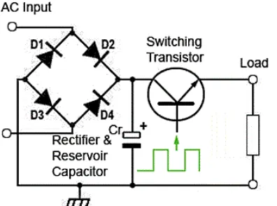
SMPS are a popular type of power supply. Compared to linear supplies, SMPS have higher efficiencies and are only a fraction of the size and weight. However, there are also disadvantages. One of the disadvantages is that SMPS are a major source of both conducted and radiated emissions [2] [3]. In this thesis the focus is on conducted emission, since the purpose is to see what the effect is if the orientation of a PLF is changed, so mirroring the filter. There is a wide variety of SMPS topologies, some of the common topologies are the buck converter, the boost converter, the buck-boost converter, the fly-back converter, the forward converter, the half bridge converter, the full bridge converter, and the resonant converter. In general a full-wave bridge will be attached to rectify the AC voltage, followed by a capacitor which stores the energy to produce a DC voltage. Here comes one of the noises, the harmonic distortion. For an SMPS a pulse width modulation (PWM) signal is used to the input of the switching transistor, either a bipolar transistor or a metal oxide semiconductor field effect transistor (MOSFET), with a voltage level at the load which is the average value of the PWM signal. The basic schematic of a SMPS is shown in Figure 2-1.
full wave rectification of the power line voltage feeding a capacitive input filter result in current spikes on the power line at the peaks of the voltage cycle as the filter capacitor recharges. The current is not drawn over the entire cycle and this is causing the current waveform to have a large amount of harmonic distortion, which can cause overheating of the transformers.
Figure 2-1 Basic schematic of SMPS.
Figure 2-2 Switched-mode power supply input waveforms.
The variable duty cycle of this PWM provides regulation for the output voltage. This switching frequency varies between a few kHz up to some MHz, and of course the rectangular wave has a large amount of harmonics. This is another part where the noise of a power converter comes from.
However, in the better topology of a SMPS (Figure 2-4) a power factor correction (PFC) is implemented. The purpose of the PFC is to minimize the input current wave form distortion and make it in phase with the voltage [10]. An example of waveforms with/without PFC is shown in Figure 2-3.
Figure 2-3 Example of waveforms with and without PFC [11].
Different SMPS will be used for this measurement. A block diagram of one of the SMPS is shown in Figure 2-4. This is a primary switched-mode power supply, which means that switching occurs on the primary side of the transformer. Usually a heat sink is connected to the body of the switching transistor (MOSFET), which dissipate the heat. Ordinarily this heat sink is not directly connected to the switching transistor, but is insulated from it by a dielectric washer. This produces a parasitic capacitance between the switching transistor and the heat sink. For safety reasons, this heat sink is mostly attached to the yellow/green wire (or the enclosure), which creates a path for common mode currents.
At the secondary side, the pulsating waveform produced is rectifies by a full-wave rectifier, smoothed by bulk capacitor and filtered by the low-pass filter. The transformer can have multiple secondary windings, numerous DC voltages of different levels can be obtained.
Figure 2-4 Block diagram of PHOENIX power supply [12].
Any SMPS configuration has multiple sources of noise. Some of these are the result of the normal operation of the circuit (Differential Mode noise), whereas others are the result of circuit’s parasitic capacitances (Common Mode noise). The power supply generates both CM and DM noise current at harmonics of the switching frequency. Although the inherent design of the power supply provides some degree of noise suppression, in almost all cases an additional PLF will also be required for regulatory compliance.
2.2 Power line filters
An EMI filter for a power supply normally consists of passive components, including capacitors and inductors, connected together to form L-C circuits. Figure 2-5 shows the general topology of a PLF. The two line-to-earth capacitors, also called Y-capacitors (C1 and C2), and the common mode choke (CMC) L1 form the common mode section of a low-pass L-C filter. Y-capacitors are the capacitors connected between AC lines and the earth. Leakage current corresponding in frequency and voltage to the AC power supply flows in the Y-capacitors. As the capacity of a Y-capacitor grows, leakage current also increases. This can cause electric shock, therefore safety standards restrict the capacity so that the amount of leakage current does not exceed a certain level. Usually, two Y-capacitors are used in PLF, as shown in Figure 2-5. These capacitors are effective in attenuating asymmetrical (common mode) interferences.
resistor Rp is usually connected parallel to C3 in order to discharge the capacitor when the filter is disconnected from the mains (see Figure 2-5).
Figure 2-5 Generic power line filter topology.
The EMI measured at line and neutral consists of the common mode (CM) and Differential mode (DM) noise. These EMI components have different sources, follow different paths and mainly attenuated by different parts of the power line filter.
2.2.1 Common Mode Filtering
CM current flows in the same direction on both power conductors (line and neutral) and returns via the earth conductor. The PLF interference can be suppressed by the use of inductors placed in series with each power line and by Y-capacitors that are connected from both power line conductors to earth [13], shown in Figure 2-6. The Lcmof CMC can be determined by using Eq. 1.
𝐿𝐶𝑀 =
𝐿 + 𝑀 2
(1)
𝑀 = 𝑘 · √𝐿1𝐿2 (2)
Where L is the inductance per winding, which is considered to be equal in both windings, and M is the mutual inductance between the two windings.
In case of a perfect choke, M is equal to L. This can be seen in Eq. 2, where the k is the coupling coefficient which represents the percentage of coupling between the two windings. In case of an ideal choke there is 100% coupling, thus k = 1. Thus for k = 1, L = M, Lcm = L.
Figure 2-6 Common mode filter.
2.2.2 Differential Mode Filtering
Differential mode current flows through one AC conductor and returns along another and can be suppressed by the filter which contains an X-capacitor connected between the two current carrying conductors, shown in Figure 2-7. A better filter can be made when space and weight is available for a line inductor, often called line choke. But in many applications the space, weight and budget is too limited to
use a line choke, and then the only option is the Cx capacitor. The LDM is the leakage inductance of CMC, this could be determined by using Eq. 3. Same as by the CM, L is the inductance per winding, and M is the mutual inductance between the two windings.
𝐿𝐷𝑀= 2 (𝐿 − 𝑀) (3)
As mentioned in Section 2.2.1, by a perfect coupling of CMC, L = M, LDM = 0.
Figure 2-7 Differential mode filter.
2.2.3 Normal mode or non-symmetrical
In a simple AC power distribution system, there are usually three wires as shown in previous sections. There is an active or live wire (also known as the hot wire), a neutral wire and an earth wire. Power is delivered to the load using the active and neutral wire. The earth wire is for safety purposes. Noise which can be measured between the active or neutral wire and earth is called normal mode (NM) noise. The NM noise is a combination of the CM and DM noise. We are interested in the NM as this voltage is measured using regulatory test standards. A comparison of DM, CM and NM is shown in Figure 2-8.
Figure 2-8 Schematics of different mode [5].
2.3 Parasitic elements
In real life ideal circuit elements do not exists, as every electrical element has parasitic elements adding undesirable effects.
An inductor has a parasitic capacitor in parallel, shown in Figure 2-9a, which will become dominant at a certain frequency. A well know characteristic of inductor is show in Figure 2-10. These can be calculated by using Eq. 4, where 𝜔 is the angular frequency, L is the inductance and C is the capacitance.
𝜔𝐿 = 1 𝜔𝐶
Figure 2-9 (a) Equivalent circuit of an inductor. (b) Equivalent circuit of capacitor.
Figure 2-10 Plot of frequency dependent behavior of equivalent circuits for various inductors [14].
A capacitor has a parasitic inductance in series, shown in Figure 2-9b. Its realistic behavior is shown in Figure 2-11, and the component values can be determined using Eq 4.
Figure 2-11 The effect of ESL for capacitance in IL [15].
3 SIMULATION
A basic schematic of a one stage power line filter is simulated. The component values of the FN 2010-16 are used [6].
Traditionally, the insertion loss (IL) has been used to characterize a PLF. Thanks to the complex structure a PLF has different CM and DM network parameters, consequent the different CM and DM IL. IL data of NM are a lower value than CM and DM IL. The reason is that the EMI
consists of both the CM and DM noise, which have different origins/sources and flow through different paths. The total EMI in line and neutral (in the NM) depends on the magnitude and phase of the CM and DM noise current. For the design of a PLF it is important to separate the conducted emission into their components [16]. However, the purpose of this thesis is not to design a PLF, but to compare the filter characteristic of an existing PLF when the orientation is changed. Therefore, the NM comparison is more useful here.
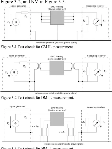
[image:6.595.314.549.207.518.2]Simulations of CM, DM and NM are done according to the test circuits in CISPR17 [17]; CM in Figure 3-1, DM in Figure 3-2, and NM in Figure 3-3.
Figure 3-1 Test circuit for CM IL measurement.
Figure 3-2 Test circuit for DM IL measurement.
Figure 3-3 Test circuit for NM IL measurement.
The six simulation circuits are shown in Figure 3-4. According to CISPR17 [17], the IL can be determined by Eq. 5, where Vo is the open circuit output voltage of a 50 Ω signal generator, and V2 is the voltage at the output of the filter circuit.
𝐼𝐿 = 20 log 𝑉𝑜 2𝑉2
(5)
Figure 3-4 Circuit diagrams used during simulation (a) NM. (b) CM. (c) DM.
3.1 Simulation with ‘ideal’ components
First simulation is performed when the input and output impedances are all 50 Ω. The source impedance Rs and output impedance Rl are set to 50 Ω. A mutual coupling coefficient (k) of 1 is used to couple the inductor pairs, i.e. L1-L2, L3-L4 and L4-L5. This coefficient is on a scale from 0 to 1 where 1 means perfect coupling between the inductors [18].
Simulation results of all six circuits is plotted in Figure 3-5, with the same color for the same mode. For NM it is black, CM is red and DM is blue. All triangle lines refers to mirror orientation of the PLF. As can be concluded from the results in Figure 3-5, mirroring the filter has no influence on the insertion loss.
Figure 3-5 Simulation results of different modes and different orientations for 50 Ω/50 Ω.
As already mention before, the datasheet of most PLF only provide the IL of CM and DM for a 50 Ω/50 Ω system, where the resistances correspond to the source resistance, Rs, and the load resistance, Rl. Whereas in real life the PLF operate under extreme mismatched conditions. CISPR17 [17] also provide the test method of this extreme cases, instead of measuring the insertion loss in a 50 Ω/50 Ω system the PLF is measured in a 0.1 Ω/100 Ω, and a 100 Ω/0.1 Ω system. These so called ‘approximate worst case measurements’ aim is to provide IL data closer to the real word operation [19].
Figure 3-6 shows simulation results for a 0.1 Ω/100 Ω system. The simulation results for a 100 Ω/0.1 Ω system is shown in Figure 3-7. The results is very comparable to each other, but the 100 Ω/0.1 Ω situation is actually almost 60 dB higher than 0.1 Ω/100 Ω. This is the consequence of the
impedance ratio, 60 dB = 1000 = 0.1
100. This is not the actual
effect of PLF, but due to the mathematics used in the simulation tool.
Figure 3-6 Simulation results of different modes and different orientations for 0.1 Ω/100 Ω.
Figure 3-7 Simulation results of different modes and different orientations for 100 Ω/0.1 Ω.
orientation does matter as the filter is non-symmetric. Which leads to the possibility that position of the components could help mitigating EMI by mirroring the PLF, as often the input and/or the output impedance are unknown and need to be estimated.
In the CM case, the simplified circuit was shown in Figure 2-6, one can see the asymmetric filter design. According to the theory shown in Figure 3-8, its orientation will influence its effectiveness in a non-50 Ω /50 Ω situation. Which can be directly seen in the differences of insertion loss in Figure 3-6 and Figure 3-7.
Figure 3-8 Basic filter theory [20].
3.2 Simulation with self-parasitic components However, in real life the components of the PLF also have parasitics, as explained in Section 2.3. Figure 3-9, shows the performance of the PLF according to the datasheet. Comparing Figure 3-9 and Figure 3-4, shows that there are deviations above 1 MHz. This could be attributed to parasitic effects. Simulations determining the self-parasitic components included in the circuit will be shown for CM, DM and NM in the following section.
Figure 3-9 Typical filter attenuation per CISPR 17 50 Ω/50 Ω for standard type FN2010-16 [6].
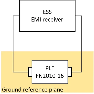
3.2.1 Common mode simulation including parasitics When the previously simulated ideal 50 Ω/50 Ω situation is compared to the data in the datasheet, for CM, Figure 3-11, one can see that parasitic elements will deteriorate the IL of the filters at high frequencies. The data of the measured CM IL comes from a measurement performed with an EMI receiver, and the test set up is shown in Figure
3-12. The measured and datasheet line are quite similar to each other, the IL for realistic filter has some resonance due to the parasitic capacitance of the inductor Cpara and the parasitic inductance of the capacitor Lpara. The circuit in Figure 3-10 is used for the simulation including parasitic components.
Figure 3-10 Example of filter with and without parasitic. (a) Ideal filter. (b) Realistic filter with parasitic elements. [21]
[image:8.595.319.511.420.612.2]Figure 3-11 Measured, simulated and datasheet CM IL for 50 Ω/50 Ω.
Figure 3-12 CM measurement setup with ESS for PLF.
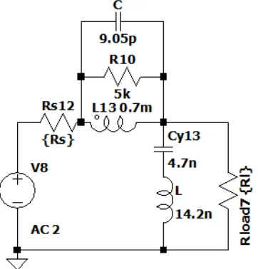
The same method is used to find the parasitic inductance of the capacitor Lpara. At 19.5 MHz again the Eq. 4 is used, but this time the C is known, and it is determined that Lpara ≈ 14.2 nH. The circuit diagram including the parasitics is shown in Figure 3-13 and the simulation result is plotted in Figure 3-14. The simulation result is much closer to the measurement results and the graphs in the datasheet now.
[image:9.595.50.231.147.336.2]Figure 3-13 Equivalent circuit for CM with parasitic elements.
Figure 3-14 Simulation with parasitic compare to measured and datasheet CM IL for 50 Ω/50 Ω.
3.2.2 Differential mode simulation including parasitics
For DM the simulation, the simulation results in Section 3.1 for 50 Ω/50 Ω is compared to the data from the datasheet in Figure 3-15. It can be seen that the simulated ideal situation has better IL especially for the lower frequencies. The simplified circuit of DM is only a Cx as already mentioned before in Figure 2-7, the datasheet shows two resonances at 2.7 MHz and 27 MHz. Using Eq. 4 again, for Cx = 0.1 µF and f = 2.7 MHz, determined L ≈ 35.7 nH. Figure 3-16 shows the equivalent circuit for DM inserted the parasitic L for C3(Cx), the parasitic for CMC is also inserted inside information box for the component itself, to keep circuit not too expanded. The simulation result after insert parasitic element is shown in Figure 3-17, somehow it looks like that there are more elements effect the DM than only one capacitance. These extra elements could actually improve the IL in higher frequencies.
Figure 3-15 Simulation compare to datasheet DM IL for 50 Ω/50 Ω.
Figure 3-16 Equivalent circuit for DM.
Figure 3-17 Simulation after insert parasitic element.
Until here it is assumed that the two inductors of CMC are identical, and the coupling coefficient (k) is 1 and all parasitic parameters are the same. Another example of DM EMI filter used for power converter is shown Figure 3-18, where DM inductance L is the leakage inductance of the coupled CM inductor [22]. A measurement was performed to try to investigate Lleakage, measurement set up is shown in Figure 3-19, result is shown in Figure 3-20. Since measurement is done with complete PLF instead of CMC itself, the result does not show the effect of the Lleakage of the CMC clearly enough to be used to derive the coupling factor.
[image:9.595.316.487.618.719.2]Figure 3-19 Measurement set up for Lleakage.
Figure 3-20 Measurement result of Lleakage.
[image:10.595.318.547.214.338.2]However in most of the cases k is very close to 1, but not equal to 1. In [23] they try to improve k > 0.9999 for planar structure CM inductor, but for non-planar structure CM inductors k < 0.999. For this simulation it is thus assumed that k = 0.999. The results are plotted in Figure 3-21, in which case the simulation and datasheet are more similar.
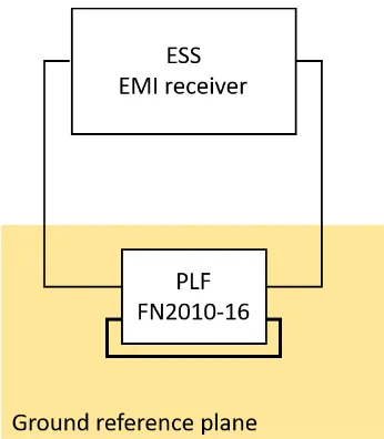
[image:10.595.48.279.290.423.2]Figure 3-21 Simulation of DM with parasitic element and Lleakage. 3.2.3 Normal mode simulation including parasitics After approximating and inserting the parasitics to CM and DM circuit, NM is also effected, Figure 3-22 shows NM without any parasitic element (orange line) and Figure 3-23 is with all the parasitic elements mentioned above. This mode is not included in the datasheet, so the comparison is between measured results and simulation. The set up for measuring the NM is shown in Figure 3-24.
[image:10.595.315.504.354.505.2]Figure 3-22 Simulated and measured NM IL for 50 Ω/50 Ω.
Figure 3-23 NM after insert parasitic elements of CM and DM.
Figure 3-24 NM measurement setup with ESS for PLF.
The simulated NM does not match the measured NM for frequencies higher than 1 MHz. It is possible that there are still some parasitics affecting this mode. As the model of the CMC could be much more complex, shown in Figure 3-25 [21].
[image:10.595.51.278.515.643.2] [image:10.595.326.487.591.756.2]3.3 Normal mode 0.1 Ω/100 Ω and 100 Ω/0.1 Ω simulation
All simulations in Section 3.2 are with the 50 Ω/50 Ω situation, since the purpose is to have a model which close to the given datasheet and measured equipment. By mirroring PLF with the 50 Ω/50 Ω system the IL does not change, even after including the parasitic components. The consequence of having different IL by mirroring PLF is not caused by self-parasitic of the components.
With this model, simulation is performed for the ‘worst case’ scenario 0.1 Ω/100 Ω and 100 Ω/0.1 Ω, and the simulation results are shown in Figure 3-26 and Figure 3-27. The results is very comparable to each other, but the 100 Ω/0.1 Ω situation is actually almost 60 dB higher than 0.1 Ω/100 Ω, this is also investigated in Section 3.1 when the components are ‘ideal’. The reason is the same, due to the impedance ratio, 60 dB = 1000 = 0.1
100. For 0.1 Ω/100 Ω,
when source impedance is low and load impedance is high, mirroring the PLF does not show improvement. For 100 Ω/0.1 Ω, is the other way around, mirroring PLF results better IL.
Figure 3-26 Simulation result for NM with parasitic elements for 0.1 Ω/100 Ω.
Figure 3-27 simulation result for NM with parasitic elements for 100 Ω/0.1 Ω.
4 METHOD
In this chapter an overview of the used instrumentation, a description of the setup elements and the description of the measurement method will be given.
4.1 Equipment
Detail of the PLF, SMPS as well as all auxiliary equipment (AE) will be described in this section.
4.1.1 Power line filter
[image:11.595.318.546.173.330.2]The PLF used in this measurement is the FN 2010-16, which is a basic one-stage filter as shown in Figure 4-1. In general the filter is installed with the Cx side to the mains (or the line, or source) input and Cy to the load (i.e. SMPS). However, it can also be mirrored by installation, with the Cyto the mains and Cxto the load. The experiment is based on these two different orientation to install the PLF.
Figure 4-1 Power line filter FN 2010.
4.1.2 Switch mode power supply (SMPS)
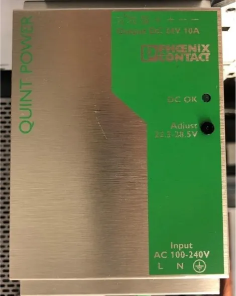
A multiple SMPS will be used during the measurements. In Figure 4-2 shows the Phoenix contact SMPS and Figure 4-3 shows two laptop chargers.
[image:11.595.50.277.327.447.2]Phoenix SMPS is selected, because it was observed that with different installation of the PLF, different filter performance was obtained. To get more comparison, two laptop chargers shown in Figure 4-3 are also selected.
[image:11.595.315.550.447.741.2] [image:11.595.49.278.487.609.2]Figure 4-3 Two laptop chargers.
4.1.3 Line impedance stabilization network
The power line impedance values ranges from about 2 to 450 Ω [2]. Because of this wide variability of power line impedances, it would be difficult to obtain repeatable conducted emission test results. To produce repeatable results, the impedance seen by a product, looking back into the AC power line, is stabilized or fixed by using a line impedance stabilization network (LISN) [2]. A LISN is a buffer network that permits connecting the power leads of the test item to the power mains by [24]:
• Passing only DC or AC power to the test sample
• Preventing the test sample’s electromagnetic noise from getting back into the power bus
• Blocking the power mains interference from coupling into the test sample
• Stabilizing the impedance presented to the test sample
[image:12.595.319.547.439.566.2]Figure 4-4 illustrate a generic example of a buffer network and Figure 4-5 illustrates the schematic for a typical 50 µH LISN.
Figure 4-4 Generic example of a buffer network [25].
Figure 4-5 Specified typical LISN for realistic impedance testing from 10 kHz to 30 MHz [25].
4.1.4 Earthing
Earthing of the test equipment and the PLF to an earth reference plane is very important for the accuracy of measurements of the low- and high-end frequency bands to eliminate spurious back earth noise and to ensure proper radio-frequency (RF) return paths. The PLF and test equipment should be secured and tested on a earth reference plane as a minimum requirement according to IEEE standard [25]. In this measurement a messing plate is used as a earth reference plane.
4.1.5 PicoScope
As a receiver, PicoScope 2208B is used in this measurement. The test setup will be show in Section 4.2. On the input of the PicoScope, a 20 dB attenuator is used. This is inserted to prevent impulse transient from the test circuit. As shown in the previous section a SMPS is used during the measurement, which means this will switching on and off due to the frequency of the SMPS itself, and by switching arises the transient. The input of PicoScope could not handle that high signal, where the 20 dB attenuator will prevent damage of the input ports.
4.1.6 Load
Power resistances are used as load in this measurement. These resistors are chosen for the large dissipation, of 50 Watt, they can handle. Instead of using one 22 Ω resistor, four are used to increase dissipation power but maintain the restive value. Figure 4-6 shows the measured frequency response characteristic of the load. Above 10 MHz it might have some non-ideal behavior due to parasitic capacitances circumventing the resistance.
Figure 4-6 Resistance characteristic.
4.2 Test setup
[image:12.595.47.275.600.741.2]setup will remain the same. Basically, the difference between the filter in normal way and mirrored, is the position of the Cx capacitor. The original idea of this measurement is also to see if changing Cx in position or even in value will contribute to higher or lower emission/immunity effect.
[image:13.595.44.279.142.220.2]Figure 4-7 Test setup used to defined how SMPS act without any filter.
Figure 4-8 Test setup used with Power Line Filter.
Figure 4-9 Power line filter installed in normal direction (upper) and mirror direction (lower).
4.3 Method of test
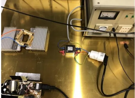
The impedance of the signal shall be 50 Ω. To ensure the input signal’s stability, a LISN is connected. The test setup is built up as shown in Figure 4-7 and Figure 4-8. The data is measured by PicoScope and will be further processed with Matlab® to compare differences of results. An example of test bench is shown in Figure 4-10.
Figure 4-10 Test bench with power line filter and laptop charger.
5 RESULTS
In this chapter all measurement results will be described and compared for different SMPS, either with and without the PLF.
5.1 Phoenix
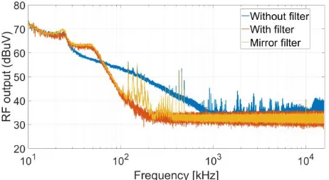
As mention in previous chapter, this SMPS is selected, because a difference between installing the PLF in ‘normal’ and ‘mirror’ configuration was observed. When the PLF was mirrored, the emission level was reduce more than 10 dB, as shown in Figure 5-1 with green line representing the normal orientation of PLF and purple for the mirrored orientation. The measurement result of Phoenix SMPS is shown in Figure 5-2, this SMPS is actually not the exactly same one which had observed the effect of mirroring.
Figure 5-1 Observed change in output of different orientations of PLF [5].
[image:13.595.49.277.346.544.2] [image:13.595.315.547.448.568.2]Figure 5-2 Measurement results of Phoenix SMPS.
5.2 Laptop charger
The same measurements are repeated but now laptop chargers are used. Two different laptop chargers are measured and the results will be shown in this section. 5.2.1 Charger 1
Figure 5-3 shows three measurement results. The blue line refers to the measurement without the PLF. The orange line and the yellow line refer to the normal orientation of PLF and the mirrored orientation of the PLF. Figure 5-4 shows the IL of PLF, by subtract output with PLF to the output without PLF, i.e. yellow line minus blue line and orange line minus blue line. The IL of mirrored and normal orientation of PLF are differences at frequency from 100 kHz to 500 kHz, but this difference is not extremely large. Figure 5-5 shows a typical circuit of a computer power supply, and this shows that at the input of the power supply already a filter (red circle) is included. Therefore, the effect of inserting a extra PLF minimalistic. Since this measurement is really aimed to show what influence the PLF could have, some modification is made to the laptop charger.
Figure 5-3 Measurement laptop charger without modification.
Figure 5-4 Determined IL with the measured output of Figure 5-3.
Figure 5-5 Typical power supply unit of computer [26].
Figure 5-6 shows the picture of the charger when it is open. The modification made here is to disassemble the Cx(in red circle) from the printed circuit board (PCB) inside the laptop charger.
Measurements were taken with and without the Cx capacitor, and the results are shown in Figure 5-7. The blue line is the same as the one in Figure 5-3 without the filter, the other two lines is when the enclosure is open (orange) and when Cx is disassembled from the PCB. It shows that only by opening the enclosure the noise level is increased. When the Cx was disassembled, it get more worse, as expected.
Figure 5-6 Laptop charge circuit.
Figure 5-7 Different situations of laptop charger without filter.
Figure 5-8 Measurement results of open enclosure with/without and mirrored filter.
Figure 5-9 Determined IL with the measured data from Figure 5-8.
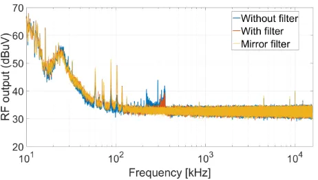
The last measurement of this charger is when the Cx is removed from the PCB. The results of this with and without PLF is shown in Figure 5-10. From this figure we can conclude that using the PLF definitely reduces the interference, and by mirroring the PLF also the interference level changed. The IL of normal and mirror filter is shown in Figure 5-11. Compare this to simulation result of NM IL in Figure 5-12, as explained in Chapter 3 the impact of 60 dB comes from the mathematical process of simulation program, the 60 dB has been normalized here. The practice measured behavior seems to be close to the 0.1 Ω/ 100 Ω situation, shown in Figure 5-13. Since for this measurement a laptop charger is used with a load which is not stable as simulation, more parasitic component is involved here. For the frequencies higher than 1 MHz, there does not show very active filtering behavior. As shown in Figure 5-10 at this frequency there output without filter does not have extremely noise to filter.
[image:15.595.49.280.62.187.2]Figure 5-10 Measurement results of without Cx with/without and mirrored filter.
[image:15.595.319.549.213.334.2]Figure 5-11 Determined IL with the data from Figure 5-10.
Figure 5-12 Simulation results for four situation of NM.
Figure 5-13 Simulation and measurement result comparison.
5.2.2 Charger 2
[image:15.595.49.277.219.347.2] [image:15.595.318.548.362.488.2] [image:15.595.47.278.585.712.2]Figure 5-14 Measurement results without Cx.
6 CONCLUSION
The research was performed due to the observation of differences in level of emission when installing a power line filter with different orientations. This effect has not been well described in literature, but observed in actual installations. In this thesis a comparison was performed between the ‘normal’ and ‘mirror’ orientation of a PLF. Simulation shown that effect of mirroring only happened by asymmetric of the source and the load impedances. When simulation were performed with equal source and load impedances, there was no change in performance observed between normal and mirror orientation of the power line filter. However, when it comes down to the so called ‘approximate worst case’ scenario, when the source impedance and load impedance are highly mismatched, i.e. 0.1 Ω/100 Ω, or vice versa, the emission levels get affected.. Insertion loss gets degraded by adding parasitcs representing non-ideal behavior of the filter. Even by adding the parasitcs the orientation of power line filter does not influence the level of emission in a 50 Ω/ 50 Ω source and load impedance situation. Again the differences in emission levels appear at 0.1 Ω/100 Ω and 100 Ω/0.1 Ω impedances scenarios. The conclusion could be drawn, that the positive effect of mirroring a filter be highly dependent on the source and load impedance. However, the effect is very identical to each other. If source impedance is high regarding to load impedance, mirroring filter will results better insertion loss. In the reverse situation, when load impedance is higher regarding to source impedance, normal orientation of PLF is recommend. Thus knowing the source impedance and load impedance of the system is very important for determining the filter installation orientation.
With a well-designed or improved switch mode power supply is not possible to investigated mirroring effect, because there is hardly any noise to filter, the build-in filter of the power supply itself already did most of the job. The results agree with the simulation results, that by mirroring the power line filter, the level of emission will change. The last step of the research would be moving Cx capacitor to the DC part of a converter (in power supply electronics). To investigate if this would result in the same or even improved EMI performance. This however could not be answered due to difficulties in modifying the DC side of the laptop power supplies, designing your own power
supply would circumvent this issue. However during the measurements, removing the Cx capacitor from the build-in filter, noise level of power supply build-increased immediately. Which indicates that having the Cx capacitor inside the power supply would reduce the level of emission, but this does not guaranty moving the Cx capacitor from power line filter to DC part of a converter will have the same effect.
REFERENCES
[1] "All about EMI filters," electronicproducts, 2008.
[2] H. W. Ott, "Conducted Emissions," in Electromagnetic Compatibility Engineering, Hoboken, New Jersey, John Wiley & Sons, 2009, pp. 492-544.
[3] C. R. PAUL, "Conducted Emissions and Susceptibility," in
Introduction to Electromagnetic Compatibility, Hoboken, New Jersey, John Wile & Sons, Inc., 2006, pp. 377-419.
[4] E. Dontigney, "How an EMI Fielter Works," SCIENCING, 24 April 2017. [Online]. Available: https://sciencing.com/emi-filter-works-5595876.html. [Accessed 17 Jan 2019].
[5] F. Leferink, "EMC filters design, applications and tricks," 2019.
[6] "Single-Stage Filters FN 2010 General Purpose AC/DC EMI Filter," Schaffner Group, 2018.
[7] "Single-Stage Filters FN 2020," Schaffner Group, 2019.
[8] "Two-Stage Filters FN 2060," Schaffner Group, 2019.
[9] "Two-Stage Filters FN 2080," Schaffner Group, 2019.
[10] S. B. Mehta and D. J. A. Makwana, "Power factor improvement of SMPS using PFC Boost converter," International Journal of Application or Innovation in Engineering & Management (IJAIEM), 2014.
[11] "PFC Switch Mode Power Supply," powersoft, [Online]. Available: https://www.powersoft-audio.com/en/technologies/pfc-switch-mode-power-supply. [Accessed 11 10 2019].
[12] "Power supply unit - QUINT-PS-100-240AC/24DC/10 - 2938604," 2019.
[13] P. Jayasree, J. Priya, G. Poojita and G. Kameshwari, "EMI Filter Design for Reducing Common-Mode and Differential-Mode Noise in Conducted Interference," International Journal of Electronics and Communication Engineering, vol. 5, pp. 319-329, 2012. [14] "Module 5:Non-Ideal Behavior of Circuit Components".
[15] "Noise Suppression by Low-pass Filters".
[16] K. S. Kostov, V. Tuomainen, J. Kyyrä and T. Suntio, "Designing Power Line Filters for DC-DC Converters," Power Electronics and Motion Control Council, 2004.
[17] "Methods of measurement of the suppression characteristics of passive EMC," IEC, 2011.
[18] M. Engelhardt, "Using Transformers in LTspice/SwitcherCAD III," Linear Technology Magazine, 2006.
[19] K. S. Kostov, J.-P. Sjöroos, J. J. Kyyrä and T. Suntio, "Selection of Power Filters for Switched Mode Power Supplies," HUT, 2014.
[20] "Basics of Noise Countermeasures," murata, 24 04 2014. [Online].
https://www.murata.com/en-sg/products/emiconfun/emc/2014/04/24/en-20140424-p1. [Accessed 12 10 2019].
[21] W. Tan, "Modeling and Design of Passive Planar Components forEMI Filters," 2010.
[22] S. Wang, F. C. Lee and W. G. Odendaal, "Characterization and Parasitic Extraction ofEMI Filters Using Scattering Parameters," IEEE TRANSACTIONS ON POWER ELECTRONICS, 2005.
[23] S. Wang, F. C. Lee and J. D. v. Wyk, "Design of Inductor Winding CapacitanceCancellation for EMI Suppression," IEEE TRANSACTIONS ON POWER ELECTRONICS, 2006.
[24] N. Violette, Electromagnetic Compatibility Handbook, Google-Books, 1987.
[25] "IEEE Standard for Methods of Measurement of Radio-Frequency Power-Line Interference Filter in the Range of 100 Hz to 10 GHz," IEEE, New York, 2006.
[26] "Power supply unit (computer)," wikipedia, 2019 August 15.
[Online]. Available:
https://en.wikipedia.org/wiki/Power_supply_unit_(computer). [Accessed 2019 09 20].
[27] "MIL-STD-220B METHOD OF INSERTION LOSS
![Figure 4-4 Generic example of a buffer network [25].](https://thumb-us.123doks.com/thumbv2/123dok_us/9657032.467702/12.595.47.275.600.741/figure-generic-example-buffer-network.webp)