1
Faculty of Electrical Engineering,
Mathematics & Computer Science
MFManufacturing: porting the
fertility chip to the standard platform
T. Feijten
Master thesis
August 2017
MFManufacturing: porting the fertility chip to the
stan-dard platform
T. Feijten, S. Dekker, A. van den Berg, M. Odijk
Male fertility testing is a cumbersome procedure, involving multiple visits to the hospital to deliver a sperm sample. The testing itself is a laborious and error-prone process. Point of care (PoC) testing can play a crucial role in making this a more comfortable and reliable experience. In the past, a system has been developed based on impedance spectroscopy to perform the diagnosis. However, it is not yet ready for PoC applications or home testing, because the current set-up is bulky. This work tackles some of the problems involved, in porting it to a standard platform and increasing the measurement accuracy by implementing a differential measurement method. Impedance deviations down to 0.22‰ are detected with headroom available. This shows the potential of this solution for fertility testing.
1
Introduction
Cellanyzer BV is in the progress of developing a point-of-care (PoC) device for fertility testing based on the proof-of-concept
as shown by Segerink et al1. However, to get the product to
market a few difficulties are encountered: the results are not re-liable enough to draw definitive conclusions2,3, the peripheral devices (impedance spectroscope, transimpedance amplifier, sy-ringe pump, PC) are quite bulky, the used capillaries are prone to leakage and the electronics are prone to noise. These kind of dif-ficulties are encountered in the commercialization of many more microfluidic devices4. To get towards a device that can be used in a PoC setting, these difficulties will have to be dealt with.
1.1 Fertility testing
For many couples wanting to start a family (1 out of 65), fertility is an important issue. In most cases, the first diagnostic test to be run concerns the sperm of the man, as this is easily testable and a main inhibiting factor in 30% of the cases5. In this test, the amount and motility of the sperm is investigated. The reference values for this, as given by the World Health Organisation (WHO) in 2010, are15·106spermatozoa per mL or more, of which 40%
or more should be motile5.
The current golden standard for diagnosing these parameters is by getting a sperm sample from the man, which is then partly in-jected in a haemocytometer (microscope slide with measurement grid and known volume per unit area) and stained. The cells are then counted and classified as being motile or non-motile5. As this is a time-consuming (therefore costly) process in which the probability of human error or difference in opinion is large, it is not an optimal process.
To solve some of the problems stated in the previous paragraph, an objective method has been developed. This method is based on the established concept of microfluidic Coulter counters, which
are devices that measure the impedance change due to an object moving along two electrodes. For an equivalent circuit diagram without a cell, see Figure 2. When a cell passes the area be-tween the electrodes, the resistance ofRel changes, which can
be detected1. To validate the performance of such devices, of-ten microbeads made from polystyrene are used. These devices have been shown (amongst others) to work for assessing yeast cell growth6, assessing airborne mineral dust7 and cell count-ing1,8, which can also be integrated on CMOS-platforms9.
To measure the impedance, a couple of methods can be uti-lized. Simply said, one needs a potential difference and a current (Z(t) =UI((tt))) to determine the impedance. Potentials are com-monly used to actuate, therefore, in a simple set-up, only the current needs to be determined (2-wire measurement). In a 4-wire measurement, the potential difference is determined as well to increase the accuracy. In this work, a 2-wire measurement will be used. To determine the current, one can use a resistor to convert it to a potential difference, which is easy to convert to a signal using, for instance, an Analog to Digital Converter (ADC). However, this resistor will influence the potential difference of the electrode pair on the fertility chip, leading to problems when non-linear effects are in place. To circumvent these problems a Transimpedance Amplifier (TIA, see Figure 1) can be used, which uses an op amp to convert the current to a potential difference. Because of the high input impedance of the op amp, the current will flow through the feedback resistor, causing an output poten-tial which can be measured. Resistors are prone to thermal noise, which can be a problem for very noise-sensitive applications. As capacitors don’t have this issue, alternative implementations have been suggested to be used as a TIA, using capacitors as feedback system10–13.
lock-− + RFB iin V + − vout
Fig. 1Traditional transimpedance amplifier circuit to convert a current to a potential difference. Due to the high input impedance of the op amp, the current will flow through the feedback resistor, leading to a potential difference at the output terminal.
in amplifier can be utilized. Using mixing and filtering, out-of-band noise is decreased drastically, which increases the signal-to-noise ratio (SNR)14.
In the system, the information is contained in the change of impedance, which can be as small as 0.1‰. The background impedance of the electrolyte and other parts of the system, there-fore, is not important, but it takes up a major part of the dynamic range of the measurement device. To optimize the measurement for the dynamic range of the lock-in amplifier and reduce noise, it is worthwhile to set up a differential measurement15.
1.2 Standardization
For microfluidics, no easy prototyping process exists. The main reason for this is that standard components, performing a spe-cific function (for instance mixing, separating or sensing), are not available. This also means that interconnects are not standard-ized, leading to difficulties when integrating components pro-vided by external parties. This is detrimental for the fabrication of prototypes, making it very hard to go from an idea to production-ready prototype.
To solve these problems, a system analogous to electronics could be used. In electronics, the usual design strategy is to de-sign a circuit using commercial off-the-shelf integrated circuits (ICs) and discrete components, such as capacitors, resistors and diodes. This design can then be implemented by producing a printed circuit board (PCB), on which the ICs and discrete com-ponents are soldered. This makes for a very flexible and quick prototyping process, which drives the industry.
Multiple solutions for this problem have been proposed16, in-cluding a modular hybrid platform using flexible PCBs, which im-proves the integration of electronics and microfluidics17, spin-ning plastic disks, which are a step ahead of prototyping, fo-cussing on mass production18, reconfigurable digital chips for PoC testing, which are mainly suited for fluidic mixing and sample preparation19and paper-based devices, which are interesting for resource-limited settings, quantitative readouts can be achieved via external devices20.
This work will use the prototyping platform designed by the MFManufacturing consortium21,22. It consists of an inherent split between functional blocks (Microfluidic Building Blocks, or
MF-BBs) and interconnects (Fluidic Circuit Board, or FCB). The in-terface of the MFBBs follows a standard, making it fairly easy to design and fabricate an FCB on which the desired MFBBs can be placed. The MFBBs can then be bought from an external party, analogous to ICs, and the FCB doesn’t contain any functionality except for interconnections, making it easy to design. This mod-ular platform is very well suited for development in a lab setting. To accelerate the maturation of this platform, projects like this work can use it to test the platform and improve the applicability.
1.3 This work
To get the fertility device ready as a prototype, this work will propose and implement some improvements. To improve the re-liability of the results and the sensitivity of the electronics, a new differential circuit will be designed, produced and tested. To re-move the capillaries and reduce the size of the peripherals, the device will be implemented based on the MFManufacturing plat-form.
First an explanation of the design choices and some simula-tions will be given, after that the practical considerasimula-tions will be treated. Then, the results will be discussed. Finally, a conclusion will be drawn and some recommendations for future research will be given.
2
Design & Simulation
2.1 Design requirements
Considering the information given in the introduction and general considerations for a PoC device23, a set of requirements can be composed for the system:
1. The system should incorporate the 15x20mm fertility chip as made by Segerink et al1;
2. The system should be compliant with the standard as set forth by MFManufacturing21,22;
3. The system should reliably determine the concentration of a sperm sample within a margin of104cells per mL;
4. The measurement result is available at most 5 minutes after introduction of the sample;
5. Between loading the sample and reading out the measure-ment, no user interaction should be needed;
6. The system can function at temperatures between10◦Cand 40◦C;
Using these requirements, a system has been designed. It con-sists of an FCB which can accommodate the fertility chip, and assisting electronics for the first signal processing, after which the signal will be processed using the lock-in amplifier.
2.2 Impedance detection
Fig. 2Equivalent circuit diagram for the fertility chip1
(a)Without cells present
(b)With cells present
Fig. 3Field lines inside the fertility chip channel (not to scale, adapted
from Segerink5)
a planar electrode configuration and a homogeneous filling with electrolyte. As can be seen, the field lines are denser near the electrodes (the field is non-homogeneous), but they do extend to the top of the channel, meaning that detection is possible in the whole channel. If a cell or insulating bead passes, as depicted in Figure 3b, part of the electric field is shielded, leading to a higher impedance. Because the field is non-homogeneous, the position in the channel where the cell or bead passes affects the response to the passage. However, this is assumed to be a small effect, so it will not be taken into account for the rest of this analysis. Depending on the cell type and whether the cell is alive, the cell behaves like an insulating shell up to3 MHz24, after which the cell will start conducting and no effect will be seen.
The expected background impedance can be estimated using the equation for resistance:
R=k·ρ (1)
in whichkis the cell constant andρ is the resistivity. The cell
constant can be determined for planar electrodes using equations given by Olthuis et al25. For electrodes with a length of18µm, width of20µmand spacing between the electrodes of30µmthese give a cell constant of approximately 37.8×10³m−1. With an electrolyte with a conductivity of1.4 S m−1, this leads to a resis-tance of26.989 kΩ(Rel). The impedance of the double layer ca-pacitance (which ranges from10µF cm−2to20µF cm−25), ranges
−
+
RREF
RT IA
−
+
RDU T(t)
RT IA
− +
inst-amp
V
vin(t)
On FCB
Fig. 4Measurement circuit topology to perform differential impedance measurements
from10.5 kΩto21 kΩfor this configuration at the measurement
frequency of100 kHz. Therefore, the background impedance is
expected to be about60 kΩ. This is in the same order of
mag-nitude as the impedance measured by Segerink et al1, which is about80 kΩ.
In order to find the impedancechange for beads with a
cer-tain volume, the Maxwell mixing theory can be used26. When a
particle is present in the electrolyte, the resistance changes:
Rel+b=Rel·
2σel+σb+Φ(σel−σb)
2σel+σb−2Φ(σel−σb)
(2)
in which σel the conductivity of the electrolyte, σb the
con-ductivity of the bead and Φ the volume fraction of the bead.
When using a realistic value for the conductivity of polystyrene (3×10⁻²⁵S m−127), the resistance changes to27.017 kΩ. This means that the resistance difference will be about28Ω, or about
0.5‰ for6µmbeads. For boar spermatozoa with a volume of
about 10 fL28, this results in a resistance change to 27.009 kΩ, meaning that the resistance difference will be20Ωor 0.33‰.
2.3 Electronics
The input Analog to Digital Converter (ADC) of the impedance spectroscope has a resolution of 12 bits. This means, that if the base resistance of the electrolyte would exactly cover the input range of the ADC, the minimal change possible to detect would be
80,000
212 ≈19.5Ω. Therefore, a passing sperm cell would only cause
Fig. 5Simulation of the circuit response, showing the response of the measurement circuit to a changing resistance added to a base
resistance of80 kΩ
high, the probability of two cells passing the electrodes in both channels at the same time is high, meaning that a reliable mea-surement is no longer possible. If this is kept low enough, this should not be a problem.
In order to achieve the differential measurement some elec-tronics topologies have been designed. More information, sim-ulations and a comparison can be found in the Supplementary Information: SI.1. The chosen topology using an instrumentation amplifier will be treated here.
In this topology, the full differential measurement is not im-plemented because the part of the circuit to be integrated on the FCB does not fit within the space constraints. This means that the solution presented will not lead to the best cancellation of the background resistance. It will, however, still lead to a substantial improvement with respect to the non-differential measurement because the output signal will be more optimal for the input range of the impedance spectroscope. See Figure 4, in whichRDU T(t)
is the impedance of the fertility chip,RREF is a (fixed) reference resistance of about the same value as the background impedance at the target frequency,RT IAis the feedback resistor for each TIA, chosen to be equal, andinst-ampis an instrumentation amplifier to determine the difference between the output potential of the two TIAs, which can then be sensed. This way, only the difference in resistance will result in a measurement potential at the output of the instrumentation amplifier, meaning that the full dynamic range of the lock-in amplifier can be used.
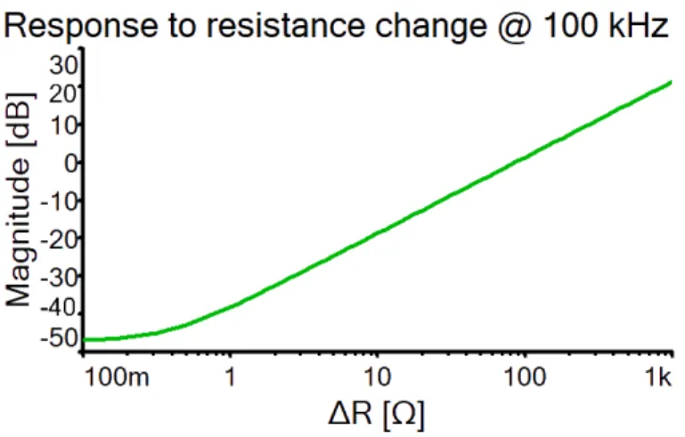
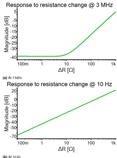
To find out the optimal component values for the topology, the circuit has been simulated using National Instruments (NI) Mul-tisim 14.1. A parameter sweep simulation has been set up, to vary the resistance indicated asRDU T(t)in Figure 4 from0.1Ωto 1 kΩ, added to a fixed baseline resistor of80 kΩ. For 20 points per decade, the response of the system is simulated and plotted in Fig-ure 5. The simulations are taken at a constant frequency of 100 kHz, with an excitation potential of 2Vpp (taken as an example, should be representative for all excitation potentials). As can be found in this graph, the system starts working linearly from a re-sistance difference of0.5Ωup to1 kΩ, which means that it should be able to detect the resistance differences as calculated. Below
(a)Reservoir (b)Flow sensor (c)Output
Fig. 6Sample MFBBs made by Dekker et al29
− + RREF RT IA − + RDU T1(t)
RDU T2(t)
RDU T3(t)
RT IA
− +
inst-amp
V
vin(t)
On FCB
Fig. 7Full measurement circuit, including additional gain and switchable channel selection
0.5Ωa response is visible, but it is not linear. As can be seen in the additional simulations done in the Supplementary Informa-tion: SI.1, this behaviour is dependent on frequency, leading to think that the bandwidth of one of the amplifiers would be the limiting factor.
In order to broaden the range of applications, additional gain could be needed. Preferably, this can be configured without the need to (de)solder a component. Therefore, a variable gain am-plifier is included in the final design, which can be set to a gain of 1 to 100 times using DIP-switches. Another consideration is how to select which channel on the fertility chip is used as the mea-surement channel. Preferably, this can also be configured without (de)soldering. In the design, this is also implemented using DIP-switches. For the full functional design of the electrical part of the system, see Figure 7. In this figure, each channel on the fertility chip is shown as an impedance, calledRDU T n(t)with n from 1 to 3. The design uses a card edge connector to connect the FCB to the rest of the system. More information on the implementation of the non-FCB electronics can be found in the Supplementary Information: SI.3.
2.4 Microfluidics
Fig. 8FCB design, showing the microfluidic connections (in blue) and the first TIA (in green). The dimensions are 85 by 54 mm.
the rest of the electronics by the use of conductive paste. Since the resulting current through the fertility chip will be small (about 200µAor lower), therefore prone to noise, it is critical to detect this current as close to the fertility chip as possible. Therefore, a TIA to convert the current to a potential difference is integrated on the FCB, marked as ’On FCB’ in Figure 4. For more information about the FCB design, see Supplementary Information: SI.2.
In the research done by Dekker et al29, some MFBBs have been developed:
• A reservoir which can be attached to a pressure pump, to induce a flow in the system, see Figure 6a;
• A differential flow sensor, see Figure 6b;
• A simple block to transport liquid to a waste reservoir, see Figure 6c.
These MFBBs can be used to introduce a sample to the fertility chip and measure the flow going through it. To keep the dead volume small, the connecting fluidic channels should be as small as possible, without risking a blockage. Therefore, their dimen-sions are chosen to be200µmfor the depth and the width, as this is the smallest mill available and blockage is not a risk for this dimension. The available flow sensor has a measurement range of0µL min−1to100µL min−1, but the fertility chip was only used with a maximum of0.1µL min−1. In order to regulate the flow going through the fertility chip to a level detectable by the flow sensor, a bypass has been added. The fertility chip will receive 1.2 ‰ of the total flow (determined by calculating the hydrody-namic resistances of the different paths30), meaning that the flow range (maximum of83µL min−1) will be in accordance with the measurement range of the flow sensor.
The microfluidic in- and outlets of a MFBB are connected to the FCB by using O-rings with an outer diameter of3.6 mmand inner diameter of1.2 mmat the interface, to prevent leakage. Similarly, if an in or outlet is not to be used, it can be closed using a block-ing element of the same outer diameter as the O-rblock-ing, but without the hole in the middle. In order for these solutions to work, a me-chanical pressure must be applied to the MFBB to close the inter-face between O-ring/blocker and MFBB/FCB. This can be done by utilizing a clamp, which can be screwed on the backplate of the FCB. For the existing MFBBs, existing clamps for 15x15mm
Fig. 9Clamp design for the fertility chip of 15 by 20 mm
blocks could be used. For the fertility chip, however, a custom clamp must be used as the dimensions are 20 by 15 mm. See Fig-ure 9 for the design of this clamp, more information can be found in Supplementary Information: SI.4.
3
Materials & Methods
3.1 Electrode material
In order to interface the fertility chip and make an electric cir-cuit on the FCB, a conductive paste will be used. Two of those were available, one with carbon graphite as a conductive ele-ment (Gwent Electronic Materials, C2000802P2) and the other with silver/silver chloride as a conductive element (Gwent Elec-tronic Materials, C2051014P10). An experiment has been devised with a credit-card sized (85x54mm), 1 mm thick wafer (Topas grade 6013, Denz BIO-Medical, Austria) of Cyclo Olefin Copoly-mer (COC) on which channels are milled with a variety of di-mensions, in which the paste can be applied and cured. Using an Agilent 34401A multimeter in resistance mode and two mea-surement probes, the resistivity will be characterized. For more information on the pastes, see Supplementary Information: SI.6.
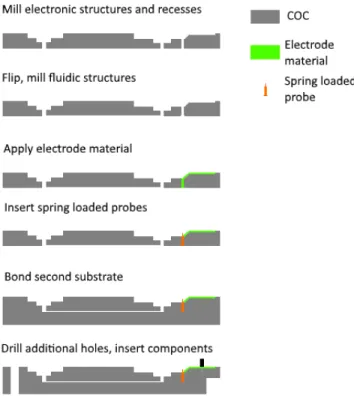
3.2 Fabrication
The design for the FCB was made in SOLIDWORKS 2017 and ex-ported to milling instructions using Autodesk HSMWorks 2018. These can be used to produce the FCB using a Sherline milling machine and a PC with LinuxCNC, starting with a 2mm thick credit-card sized COC substrate. For more information about mi-cromilling, see Supplementary Information: SI.5. See Figure 10 for a schematic overview of the fabrication process. After milling the substrate on both sides, the conductive paste will be applied around the spring probe locations and the spring probes (Smiths Connectors, 101582) will be inserted. After curing the paste, an-other 2mm thick credit-card sized COC substrate will be bonded to this side using solvent bonding, sealing the channels. Subse-quently, the last holes will be drilled and some substrate will be removed in order to accommodate the card edge connector. Then the rest of the paste will be applied and two decoupling capaci-tors, two pin headers for the feedback resistor and the op amp IC will be inserted. After curing, the FCB will be ready to be used. For a full description of the fabrication process, see Supplemen-tary Information: SI.7.
us-Fig. 10Schematic overview of the fabrication process for the FCB
82 kΩ
18Ω
Fig. 11Circuit to test circuit response to a small resistance change
ing the same machine as the FCB, out of aluminium. After open-ing the window at the location of the fertility chip for easy optical access and drilling the holes, the holes will be threaded to be able to mount the FCB and clamps on the baseplate.
For the fertility chip, a clamp was needed. The design for the clamp was exported to an STL file and can be manufactured us-ing 3D-printus-ing based on a stereolithographic technique (Form-labs Form 2). For more information about stereolithography, see Supplementary Information: SI.5.
3.3 Electric validation
In order to validate the working of the electronics, a resistance test has been set up. On the FCB, a fixed resistance will be mounted of about82 kΩ instead of the fertility chip. The feed-back resistor for the TIA on the FCB will also be about82 kΩ. The circuit in Figure 11 will replace the reference resistorRREFin Fig-ure 4. If the button is pressed, the total resistance will decrease with an amount of18Ω, which has the same effect as an increase of this amount inRDU T. This way, the effect on the measurement of a resistance change can be investigated. The measurement fre-quency to be used will be 100 kHz, and the actuation potential difference will be0.3 VRMS.
3.4 Fluidic validation
For validating the working of the system for its final purpose, a test using beads has been set up. A suspension of6µmdiameter dyed red beads (Polysciences Inc, 15714) with a concentration of106mL−1in Phosphate Buffered Saline (PBS) (Sigma Aldrich,
P4417-100TAB) will be introduced to the system. This is done using the MFBBs described in subsection 2.4, mounted on the FCB using the mentioned clamps, O-rings (Eriks BV, AS568-002) and blocking elements (which can be fabricated using PDMS and a mould). A Fluigent MFCS-4C pressure pump will be used to push the solution through the system.
4
Results & Discussion
4.1 Electrode material
When looking closely at the substrates, of which pictures can be found in Supplementary Information: SI.6, some of the channels on the carbon graphite plate contain holes, caused by some of the paste being removed out of the channel by the windscreen wiper. The silver/silver chloride substrate doesn’t seem to suf-fer that much from this problem. The results can be found in Figure 12 for the carbon graphite paste and Figure 13 for the sil-ver/silver chloride paste. As can be seen, the resistance of the carbon graphite channels is much higher than the resistance of the silver/silver chloride channels. Furthermore, some of the car-bon graphite channels have a much higher resistance than would be expected, which can be explained by the holes mentioned pre-viously. Based on these results, the paste based on silver/silver chloride will be used as electrode material.
4.2 Fabrication
The FCB and additional electronics have been fabricated, see Fig-ure 14. Some dimensions have been measFig-ured to verify the de-sign to product workflow. For a measurement of the fluidic chan-nels, see Figure 15a and Figure 15b. The designed channel width is200µmfor the main channels, leading to a deviation of 62.3% for the top channel and 37.0% for the bottom channel. The de-signed bypass width is800µm, leading to a negative deviation of
y = 466,67x-0,696
R² = 0,7357
0 1000 2000 3000 4000 5000 6000
0 0,1 0,2 0,3 0,4 0,5 0,6 0,7
R esit anc e [ Ω ]
Channel cross sectional area (µm²) Resistance for carbon graphite electrodes
y = 0,298x-0,824 R² = 0,9852
0 0,5 1 1,5 2 2,5 3 3,5 4 4,5
0 0,1 0,2 0,3 0,4 0,5 0,6 0,7 0,8 0,9
R
esi
st
ance
(
Ω
)
Channel cross sectional area (µm²) Resistance for silver/silver chloride electrodes
Fig. 13Resistance vs channel volume for silver/silver chloride electrodes
Fig. 14Overview of the whole system
33.7%. Revisiting the calculations in subsection 2.4, the fertility chip will receive 2.08‰ of the total flow, meaning that the total flow will have a maximum of48.2µL min−1, limiting the dynamic range of the flow sensor.
For a measurement of the clamp side, see Figure 15c. The
designed top dimension is 800µm and the total dimension is
1930µm, leading to a deviation of 6.5% and 2.5%, respectively. Deviations in this part could lead to a MFBB not fitting inside the clamp, which could lead to problems mounting the MFBB and, possibly, breaking of the MFBB. However, the deviations found are perfectly fine for this use. For a measurement of two holes in the clamp, see Figure 15d. The designed diameter of the small hole is1000µmand of the large hole is2100µm, leading to a de-viation of 15.4% and 2.1%, respectively. Dede-viations in the holes could lead to screws not perfectly fitting, and a loose clamping. However, through the countersunk design, a very large deviation is required to cause problems, which is not the case. Finally, for a measurement of an electrode channel on the FCB, see Figure 15e. The designed electrode width is400µm, leading to a deviation of 3.25%.
(a)At channel junction,
top=324.6µm, bottom=275.8µm (b)At bypass, width=530.7µm
(c)At side of clamp, top=852µm,
total=1979µm
(d)At holes in clamp, large
hole=2145µm, small
hole=1154µm
(e)At electrode, width=413µm
0,09 0,14 0,19 0,24 0,29
0 1 2 3 4 5 6 7 8
Ampl itu de [V] Time [s] Lock-in output
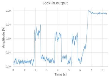
Fig. 16Results for the electric validation, in which the button was pressed three times
4.3 Electric validation
The set-up as described in subsection 3.3 has been built and used to validate the electric functionality. The filter settings of the lock-in amplifier were set to their default settlock-ings, and the additional gain amplifier was set to 5x. The results are plotted in Figure 16. Some observations can be made: the button has been pressed three times, which is clearly visible. The amplitude difference for the small resistance change is substantial, about100 mV, which is a change of about 200 ADC levels, and consistent. The signal is very noisy, from20 mVto55 mV, which is a difference of about 40 to 110 ADC levels. The system is also susceptible to external factors, which is clearly visible in the graph. At sample 2800, the hand of the person pressing the button was pulled away from the set-up, leading to a major increase in signal. However, the button press responses are clear enough to say we can reliably detect a resistance change of18Ω.
4.4 Fluidic validation
Because of time constraints, no fluidic testing was carried out.
5
Conclusions & Recommendations
Some very promising results have been acquired:
1. Integrating electrodes and even some electric components on an FCB is very well possible by using conductive paste;
2. Stereolithography can be used as a rapid production method for MFBB clamps;
3. It is shown that a resistance difference of18Ω can be de-tected on top of a82 kΩbackground;
Based on the results given above, the system is a promising set-up which can be used to get the fertility chip system towards a production-ready PoC prototype, which is the next step for the fertility chip on the way to market.
Next steps to be taken to get towards a complete solution, be-sides the recommendations made in section SI.2 and section SI.3, are:
1. Integrate a mixer MFBB to perform auto-calibration using both microfluidic beads and a sperm sample. Because we can differentiate between beads and spermatozoa, it is pos-sible to relate the concentration of sperm cells to the con-centration of beads and number of beads and spermatozoa counted in a certain amount of time. This could be done by extending the size of the FCB to accommodate two more MFBBs: the mixer and another reservoir for the calibration fluid;
2. Implement a full differential measurement using another channel of the fertility chip, in order to cancel the thermal drift and phase shifts present in the impedance of the fertility chip. This could be done by finding a way to integrate more electronics on the FCB, or by moving the measurement area to a place close to the connection of the rest of the system, delegating the conversion of the currents and the differential measurement;
3. Use the flow sensor as a feedback system to regulate the pressure pump to the wanted flow rate. This means that no longer a pressure has to be set, but a flow can be set as well;
4. Because it is very hard to mount the fertility chip without breaking it, the clamp design should be adjusted so it applies pressure on the chip (to close the O-rings), but then touches the FCB to prevent breakage;
5. The headers used for the connection of the feedback resistor on the FCB are prone to breaking, so if no changing is re-quired these should be replaced by a permanent resistor. To do this, the hole diameters need to be adjusted accordingly.
Acknowledgements
This work was supported by ENIAC Joint Undertaking (JU), a public-private partnership focusing on nanoelectronics that brings together ENIAC Member/Associated States, the European Com-mission, and AENEAS (an association representing European R&D actors in this field).
The author wishes to express his gratitude to J. Loessberg-Zahl for fabricating the clamps for the fertility chip, and to F. van den Brink for brainstorming about the electrode material.
References
1 L. I. Segerink, A. J. Sprenkels, P. M. ter Braak, I. Vermes and A. van den Berg,Lab Chip, 2010,10, 1018–1024.
2 M. J. Leene,Thesis, University of Twente, 2016. 3 E. Hoogendijk,BSc-thesis, University of Twente, 2016. 4 L. R. Volpatti and A. K. Yetisen,Trends Biotechnol., 2014,32,
347–350.
5 L. I. Segerink,PhD-thesis, University of Twente, 2011. 6 J. Sun, J. Yang, Y. Gao, D. Xu and D. Li,Microfluid.
Nanoflu-idics, 2017,21, 33.
7 F. Liu, Y. Han, L. Du, P. Huang and J. Zhe,Microfluid. Nanoflu-idics, 2016,20, 27.
9 Y. Chen, J. Guo, H. Muhammad, Y. Kang and S. K. Ary,IEEE Trans. Biomed. Eng., 2016,63, 311–315.
10 G. Ferrari, M. Carminati, G. Gervasoni, M. Sampietro, E. Prati, C. Pennetta, F. Lezzi and D. Pisignano, 2015 Int. Conf. Noise Fluctuations, 2015, pp. 1–6.
11 M. Jalali, A. Nabavi, M. Moravvej-Farshi and A. Fotowat-Ahmady,Microelectronics J., 2008,39, 1843–1851.
12 M. Crescentini, M. Bennati, S. Saha, J. Ivica, M. de Planque, H. Morgan and M. Tartagni,Sensors, 2016,16, 709.
13 M. Kubo, H. Yotsuda, T. Kosaka and N. Nakano, 2015 Int. Symp. Intell. Signal Process. Commun. Syst., 2015, pp. 307– 311.
14 J. H. Scofield,Am. J. Phys., 1994,62, 129–133.
15 M. Carminati, G. Gervasoni, M. Sampietro and G. Ferrari,Rev. Sci. Instrum., 2016,87, 026102.
16 D. Mark, S. Haeberle, G. Roth, F. von Stetten and R. Zengerle, Chem. Soc. Rev., 2010,39, 1153.
17 A. Wu, L. Wang, E. Jensen, R. Mathies and B. Boser,Lab Chip, 2010,10, 519–521.
18 J. Ducrée, S. Haeberle, S. Lutz, S. Pausch, F. V. Stetten and R. Zengerle, J. Micromechanics Microengineering, 2007, 17, S103–S115.
19 R. Sista, Z. Hua, P. Thwar, A. Sudarsan, V. Srinivasan, A. Eck-hardt, M. Pollack and V. Pamula,Lab Chip, 2008,8, 2091.
20 A. K. Yetisen, M. S. Akram and C. R. Lowe,Lab Chip, 2013,
13, 2210.
21 H. van Heeren, T. Atkins, N. Verplanck, C. Peponnet, P. Hewkin, M. Blom, W. Buesink, J.-E. Bullema and S. Dekker, 2016, DOI: 10.13140/RG.2.1.1698.5206.
22 H. van Heeren, T. Atkins, N. Verplanck, C. Peponnet,
P. Hewkin, M. Blom, W. Buesink, J.-E. Bullema and S. Dekker, 2016, DOI: 10.13140/RG.2.1.3318.9364.
23 V. Gubala, L. F. Harris, A. J. Ricco, M. X. Tan and D. E. Williams,Anal. Chem., 2012,84, 487–515.
24 H. Morgan, T. Sun, D. Holmes, S. Gawad and N. G. Green,J.
Phys. D. Appl. Phys., 2007,40, 61–70.
25 W. Olthuis, W. Streekstra and P. Bergveld,Sensors Actuators B Chem., 1995,24, 252–256.
26 T. Sun, C. Bernabini and H. Morgan, Langmuir, 2010, 26,
3821–3828.
27 V. Adamec,Kolloid-Zeitschrift Zeitschrift für Polym., 1970,237, 219–229.
28 A. M. Petrunkina, M. Hebel, D. Waberski, K. F. Weitze and E. Topfer-Petersen,Reproduction, 2004,127, 105–115. 29 S. Dekker, A. van den Berg and M. Odijk, 2017, DOI:
unpub-lished working paper.
30 H. Bruus, Theoretical Microfluidics, Oxford University Press, 2008.
31 Zurich Instruments, HF2 user manual -
zi-Control edition, 2015, https://www.
zhinst.com/sites/default/files/
ziHF2{_}UserManual{_}ziControl{_}45800.pdf.
32 J. O. P. Zanen,Datasheet differential source- measurement unit for resistance difference measurements, University of twente technical report, 2016.
33 B. van Dam and W. Buesink, 2017, DOI: unpublished working document.
SUPPLEMENTARY INFORMATION
SI.1
Clarification of Electronics design
In the original work by Segerink1, a home-made impedance spec-troscope was used to detect the impedance, which worked us-ing a pick-up amplifier and synchronous detection. Later on,
other home-made circuits (see for example Figure 17)2 and an
impedance spectroscope made by Zurich Instruments (see Fig-ure 18)3have been used. These solutions were all based on de-tecting the whole impedance, and dede-tecting the peaks afterwards. This means that only a small part of the whole dynamic range of the final ADC could be used for peak detection, leading to loss of precision.
To improve the detection of small variations in impedance, a couple of topologies are proposed, namely using a differential driver, a summing amplifier, an instrumentation amplifier and an inverting amplifier. These will be analyzed and simulated piece by piece, after which a comparison and conclusion will be given. All the simulations have been carried out by NI Multisim 14.1.
SI.1.1 Differential Driver
This topology, as depicted in Figure 19, is inspired by the de-sign as proposed by Zanen32. The main idea is to create a signal and its inverse based on an input sine signal, then feed it to both the device and a resistance in the same order of magnitude as the background electrolyte impedance. After these resistances, a node sums both currents to only keep the difference (which con-tains the impedance difference and therefore the signal), which is then converted to a voltage by the TIA. The impedance difference
Fig. 17One of the used home-made measurement circuits3
Fig. 18The measurement circuit using the Zurich Impedance
Spectroscope31
− +
−
+ AD8138 RDIF
vin(t)
RDIF
RDIF RDIF
RDU T(t)
RREF
−
+ LT6200
RT IA
V
Fig. 19Measurement circuit, based on differential driver
can then be determined:
RDU T(t) =Rbase+∆R(t)
RREF=Rbase
uDU T=−uin
uREF=uin
uout(t) =iT IA(t)·RT IA
iT IA(t) =iREF+iDU T(t) = uin Rbase
+ −uin Rbase+∆R(t)
uout(t) = −uin·RT IA·∆R(t) R2base+Rbase·∆R(t)
∆R(t) = −Rbase
1+ uin·RT IA uout(t)·Rbase
The circuit has been simulated, using the following values:
RDIF=470Ω,RREF=80kΩ,RT IA=3.3kΩand varyingRDU T from 0.1Ωto1 kΩwith a baseline of80 kΩ, yielding the results in Fig-ure 20. As can be seen in this figFig-ure, the circuit starts to change output at a resistance difference of about10Ω, and is linear from 300Ωup to1 kΩ.
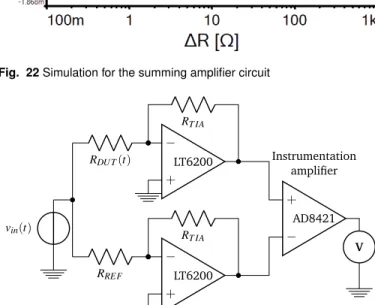
SI.1.2 Summing amplifier
Fig. 20Simulation for the differential driver circuit
−
+ LT6200
RDU T(t)
vin(t)
RT IA
RSU M
RSU M −
+ LT6200
RSU M
V
Fig. 21Measurement circuit, based on summing amplifier
voltage:
Uout=−RT IA·Iin (3)
Iin=Uin·Rdut(t) (4)
ifRT IA=Rdut(t):
Uout=−Uin (5)
We can then use a summing amplifier to subtract the input signal from the background electrolyte impedance signal, which then leaves the difference signal.
The circuit has been simulated, using the following values:
RSU M=1kΩ,RT IA=80kΩand varyingRDU T from0.1Ωto1 kΩ with a baseline of80 kΩ, yielding the results in Figure 22. As can be seen in this figure, the circuit starts to change output at a re-sistance difference of about10Ω, and is linear from400Ωup to 1 kΩ.
SI.1.3 Instrumentation amplifier
For this topology, as depicted in Figure 23, the TIA as depicted in Figure 1 is duplicated with a fixed reference resistance (in the same order of magnitude of the background electrolyte re-sistance), after which the output voltages are fed into an instru-mentation amplifier. An instruinstru-mentation amplifier is a difference amplifier, with the characteristic that no impedance matching
be-Fig. 22Simulation for the summing amplifier circuit
−
+
LT6200 RREF
RT IA
−
+
LT6200 RDU T(t)
RT IA
− + Instrumentation amplifier AD8421 V
vin(t)
Fig. 23Measurement circuit, based on instrumentation amplifier
tween the inputs is needed because of the high-impedance input buffers and the gain can be tuned very easily. It is therefore very suited for use in measurement equipment, also due to its low drift and low noise. In this topology, it determines the difference be-tween the inputs and amplifies it. This topology can also be used to reduce the noise in the conductance signal15.
The circuit has been simulated, using the following values:
RREF=80kΩ,RT IA=80kΩand varyingRDU T from0.1Ωto1 kΩ with a baseline of80 kΩ, yielding the results in Figure 24. As can be seen in this figure, the circuit starts to change output at a re-sistance difference below100 mΩ, and is linear from0.5Ωup to 1 kΩ.
SI.1.4 Inverting amplifier
This implementation, as depicted in Figure 25, follows the same inspiration as the differential driver topology, but uses a different way to generate the inverted input signal. This is done by using an inverting amplifier with amplification -1, which then drives the reference resistance. After this, the currents are again added to keep the difference between them, and converted to a voltage using the TIA.
The circuit has been simulated, using the following values:
RINV =100Ω,RREF=80kΩ,RT IA=80kΩand varyingRDU T from
Fig. 24Simulation for the instrumentation amplifier circuit
−
+
LT6200
RDU T(t)
RREF
−
+
LT6200
RINV RINV vIN(t)
RT IA
V
Fig. 25Measurement circuit, based on inverting amplifier
Fig. 26Simulation for the inverting amplifier circuit
(a)At3 MHz
(b)At10 Hz
Fig. 27Additional simulations for the instrumentation amplifier circuit
output at a resistance difference of about10Ω, and is linear from 100Ωup to1 kΩ.
SI.1.5 Comparison
SI.2
FCB Design
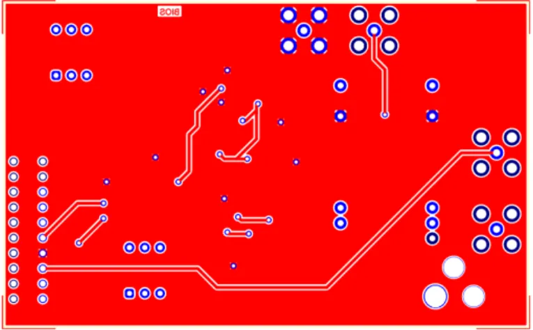
In order to introduce a sample to the fertility chip and read out the electronics, an FCB has been designed. The electrodes on the fertility chip can be interfaced using spring loaded probes (Smiths connectors), which will press onto the contact pads. These are connected to the rest of the electronics by the use of conductive paste. Since the resulting current through the fertility chip will be small, it is critical to detect this current as close to the fertility chip as possible. Therefore, a TIA to convert the current to a po-tential difference is integrated on the FCB. Furthermore, a bypass to regulate the flow going through the fertility chip to a level de-tectable by the flow sensor is included. For an exploded view of all included components of the FCB, see Figure 29. For the top view of the FCB design, see Figure 30, for the embedded channel design, see Figure 31, for the design of the backplate (sealing the channels), see Figure 32 and for the design of the baseplate on which the FCB can be mounted see Figure 33. The FCB has been manufactured and assembled, see Figure 34 for a photograph.
SI.2.1 Electronics
In order to convert the current through the fertility chip to a volt-age, a TIA is included on the FCB. The feedback resistance can be changed easily due to the pin headers in which this is mounted. Besides the red part marked ’On FCB’ in Figure 4, some power supply decoupling capacitors are included. See Figure 30 for the layout of the circuit on the FCB. The full bill of materials for the FCB can be found in Table 2.
SI.2.2 Bypass
The bypass is meant to reduce the flow through the fertility chip. The fraction of the flow that will go through the fertility chip can be determined using the equivalent circuit diagram depicted in Figure 28 and determining the various resistances30. For rectan-gular channels:
R= 12ηL
1−0.63(wh)
1
h3w (6)
in whichη the viscosity (1.0016 mPa sfor water @ 20◦C),Lthe length of the channel,hthe height of the channel andwthe width of the channel. For square channels (width equal to height) goes:
R=28.4ηL1
h4 (7)
Using the values in Table 1, the equal resistance of the part becomes1.217×1014Pa s m−3. Therefore, the ration between the flows becomes 1.24‰, which means that the total flow will be-come about80.65µL min−1for a flow of0.1µL min−1through the fertility chip.
SI.2.3 Variables
In the SOLIDWORKS model, a couple of variables have been de-fined in order to make changing the design very easy. For in-stance, if the inter-electrode spacing needs to be increased
be-Table 1Hydrodynamic resistances in FCB
Resistor w [µm] h [µm] L [mm] Resistance [1011Pa s m−3]
FCB1 200 200 29.02 5.16
chip1 = chip2 96 18 1.525 371
measurement 38 18 0.6 464
FCB2 200 200 32.5 5.78
bypass 800 200 67.67 1.51
RFCB1 Rchip1 Rmeasurement Rchip2 RFCB2 Rbypass
Fig. 28Equivalent hydrodynamic circuit diagram of FCB
Fig. 29An exploded view of all the FCB components
Table 2Bill of Materials for the FCB
Quantity Type of part Value/part nr Manufacturer Farnell order code
1 Op amp (TIA) LT6200CS8 Linear Technology 1330751
1 Female pin header (strip of 10) n.a. Multicomp 1593464
1 Resistor (feedback) 80 kΩ Multicomp 9340955
2 Capacitor (power decoupling) 100 nF Vishay 1141775
6 Spring loaded probe 101582 Smiths connectors n.a.
Fig. 31The bottom view of the FCB top plate
Fig. 32The FCB back plate, to seal the channels
Fig. 33The FCB base plate, for easy assembly
Fig. 34The assembled FCB
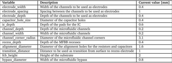
cause there are some problems, this is as easy as increasing the value of the electrode_spacing variable. For all the variables and a short description of these, see Table 3.
SI.2.4 Modifications
For the next version of the FCB, the following modifications are recommended to make:
1. Exchange the IC for a through-hole variant, to ease the man-ufacturing. Right now, the IC is used as a surface-mounted device, but it is not enough to press it in the paste while manufacturing to affix it. Therefore, currently the IC is fixed using a droplet of Hysol glue and connected to the elec-trodes using Conductive Paint, leading to a more complex production process. A through-hole IC will be fixed when it is pressed in the paste when manufacturing, simplifying manufacturing;
2. If no longer needed, remove the electrode from the negative input of the IC towards the connector to reduce noise;
Table 3Variables used in the SOLIDWORKS model
Variable Description Current value [mm]
electrode_width Width of the channels to be used as electrodes 0.4
electrode_spacing Spacing between the channels to be used as electrodes 1
electrode_depth Depth of the channels to be used as electrodes 0.4
capacitor_hole_size Diameter of the capacitor holes 0.4
ic_depth Depth of the pads for the IC 0.6
channel_depth Depth of the microfluidic channels 0.2
channel_width Width of the microfluidic channels 0.2
channel_corner_radius Diameter of the microfluidic channel corners 3.1
recess_depth Depth of the MFBB recesses 0.4
alignment_diameter Diameter of the alignment holes for the resistors and capacitors 1.6
transition_distance Distance to be used as transition from surface to recess electrode 1
fcb_height Height of the substrate 2
SI.3
PCB Design
To convert the output of the FCB electronics as explained in SI.2, a PCB has been developed which will also provide the FCB elec-tronics with an input signal and the needed power supplies. It implements the part of the electronics as described in SI.1 which is not placed on the FCB, power conversion and additional am-plification. It is also possible to choose the channel of the chip which should be used for the measurement. The design of the top layer of the PCB is depicted in Figure 35 and the design of the bottom layer in Figure 36. The full Bill of Materials (BOM) can be found in Table 5, including Farnell order code (can be used with
the URLhttp://nl.farnell.com/<order-code>).
SI.3.1 Power conversion
In order to power the circuit without the need for external sym-metric power supplies, a DC-DC converter is present on the PCB
which can be powered by 18-75 V DC and generates5 V, ground
and−5 V. In order to maximize the flexibility, a full diode bridge is present as well, meaning that the PCB can also be powered by AC (same voltage range as for DC). However, as these diodes in-duce a voltage drop of1.1 Vper piece, the voltage range which
can be used to power the circuit changes to 20-77 V (NOTE: On
the produced PCB, this is erroneously described as 11-38 V!).
SI.3.2 Gain
On the PCB, an additional gain amplifier is present. This is im-plemented using a variable gain amplifier (LTC6910) and some switches to select the gain. The switches can influence the gain in a digital way. The resulting gains can be found in Table 4.
SI.3.3 Modifications
The following modifications have been made to the original de-sign in order to get the circuit working:
1. The ground and negative power supply rails of the FCB were switched around, which has been fixed (see Figure 40);
2. On the original design, the TIA was implemented using a Texas Instruments TLC271 op amp, which did not comply
Fig. 35The top layer of the PCB
Table 4Gain for different switch positions
Switch 1 Switch 2 Switch 3 Gain [V/V]
0 0 0 0
0 0 1 1
0 1 0 2
0 1 1 5
1 0 0 10
1 0 1 20
1 1 0 50
1 1 1 100
with the bandwidth requirement. It has been switched with a LT6200 op amp, which requires pin 1 to be floating instead of connected to ground. Therefore, this pin is cut through;
3. In the simulations the instrumentation amplifier had the best performance with a very low gain resistor (very high gain). This led to offset due to noise to be amplified too much, so no usable signal could be obtained. The gain resistor was switched out for a1.2 kΩresistor, decreasing the gain of the instrumentation amplifier;
4. The output terminals are not connected to the ground, be-cause this would damage the input of the lock-in amplifier. A wire is soldered to the ground plane to make diagnosis with an oscilloscope possible, see Figure 39. A better solution to make the ground accessible is to add a header pin connected to the ground plane.
For the next version of the PCB, the following modifications (alongside the ones mentioned previously, which were only done for 1 PCB) are recommended to be implemented:
1. Shorten the trace between pin 7 of the instrumentation am-plifier and C3;
2. Either remove the FCB-out connector and associated trace, or shorten it as much as possible. This trace will introduce noise to the measured signal, as it acts like an antenna;
3. Use the lower voltage variant of the DC-DC converter (TEN 2421WI, Farnell order code 1772190, instead of TEN 8-4821WI), to lower the needed power supply voltage.
Fig. 37The top layer of the produced PCB
Fig. 38The bottom layer of the produced PCB
Table 5Bill of materials for the PCB
Quantity Type of part Value/part nr Manufacturer Farnell
order code
On-board reference
2 Capacitor (DC decoupling) 1µF Multicomp 1759454 C3, C6
6 Capacitor (power decoupling) 100 nF Multicomp 1759366 C1, C2, C5, C7,
C8, C9
1 Card edge connector (FCB) 5-5530843-0 TE Connectivity 2396188 Microfluidics
1 DC connector (power) RAPC712X Switchcraft 1608726 Power
1 DC-DC converter (generate
symmetric power supply)
TEN8-4821WI Tracopower 1772198 DCDC_conv
2 DIP-switch MCNDS-03-V Multicomp 1255223 CHAN_SELECT,
Gain_select
1 Diode bridge (AC to DC) DB102S Multicomp 1861404 Rect
1 Instrumentation amplifier AD8421ARZ Analog Devices 2126090 Instr_amp
1 Variable gain amplifier
LTC6910-1CTS8
Linear Technology 1663930 Var_amp
1 Operational amplifier (TIA) LT6200CS8 Linear Technology 1330751 TIAref
3 Resistor (pull-down) 100 kΩ Yageo 9241060 R8, R9, R10
1 Resistor (instrumentation
am-plifier gain)
10Ω Welwyn 2078988 Rg
1 Resistor (reference, should be
similar to the FCB resistance)
80 kΩ Panasonic 2307861 Rref
3 Resistor (for tuning reference
resistance)
optional n.a. n.a. RREF1, RREF2,
RREF3
1 Resistor (feedback of reference
TIA)
80 kΩ Panasonic 2307861 Rf
4 SMB connector
SMB1252B1-3GT30G-50
Amphenol 1111351 FCB_out,
SI.4
Clamp
In order to mount the chip on the FCB, a clamp has been
de-signed based on the proposal from MFManufacturing33. The
mensions were adapted to fit the fertility chip, which has outer di-mensions of 20 by 15 mm. The design can be found in Figure 41 (top) and Figure 42 (bottom). Some variables were defined in the SOLIDWORKS-model, in order to make changing the model very easy. The variables can be found in Table 6. The clamp has been manufactured using stereolithography, the result of which can be found in Figure 43 and Figure 44.
Fig. 41Top of the clamp design
Fig. 42Bottom of the clamp design
Fig. 43Top of the manufactured clamp
Table 6Variables used in the SOLIDWORKS model
Variable Description Current value [mm]
MFBB width The width of the MFBB to be used with the clamp 20.25
MFBB length The length of the MFBB to be used with the clamp 15.25
MFBB recess The recess depth for the MFBB 0.4
SI.5
Rapid prototyping
Microfluidic circuits can be fabricated using a couple of technolo-gies, such as PDMS moulding, stereolithography (3D-printing), micromilling, glass processing, paperfluidics and hot emboss-ing34. Of these technologies, stereolithography, micromilling, glass processing and hot embossing could be used to manufacture an FCB, as PDMS and paper lack the required rigidity for assem-bling MFBBs on them. A table with some of the characteristics of these methods compared can be found in Table 7.
Stereolithography is an additive fabrication method which uses a photoactivated polymer and a laser to selectively polymer-ize layers of a fluidic bath (sometimes also referred to as 3D-printing), which can be used to build up structures. It can also be used to create embedded channels, which creates the challenge of expelling the non-polymerized fluid from the channel. This makes the minimal channel diameter about500µm.
Micromilling is a subtractive fabrication method which uses mills and drills to selectively remove material from a bulk piece of material. This can be used with a broad range of materials, for in-stance polymers or metals. Using an automated milling machine, one can draw the desired structure in a CAD-program and use a CAM-program to produce the structure. The smallest structures depend on the mill size, which can get as small as200µm. Closed-off channels require the material to be bonded to another piece
of material, which can create issues with alignment of structures. Glass processing is also a subtractive fabrication method, but it entails a lot more than just creating structures. It can, for in-stance, also be used to create electrodes on the surface of the glass. Glass processing starts with a glass substrate, which can then be covered by photoresist which is selectively removed us-ing photolithography. With the resist actus-ing as a mask, glass can be removed using etching after which the resist is removed again. To create a channel, another glass substrate can be bonded to the existing structures. This production method is not really suited for large structures, as the etching and mask development for the photolithography take a long time. The channel size depends on the resist chemistry and lithography resolution. Sizes lower than 20µm can be reached easily (the original fertility chip is made using this technology).
Table 7Comparison of fabrication methods
Method Micromilling 3D-printing Lithography + etching
3D-casting + hot embossing
Cost + + – (clean room) +(+) (for high volumes)
Alignment - (multiple layers) ++ (multiple layers) - (multiple layers)
Channel size (min.200µm) - (min.500µm) ++ (min.20µm) + (min.100µm)
Speed + + - +(+) ( for high volumes)
Feature size - ++ /+
Material COP/COC Methacrylated
polymer
Glass COP/COC
Electrode integration
/- +
Biocompatibility + - + +
Chemical resistivity
SI.6
Description of electrode material
differ-ences
Two types of electrode materials were available, both in a paste form. One is based on carbon graphite (Gwent Electronic Materi-als, C2000802P2) and the other on silver/silver chloride (70/30) (Gwent Electronic Materials, C2051014P10). Their reported re-sistivities are, respectively50Ω/square and0.34Ω/square. They are made to be applied on a substrate, then cured in an oven to set and attach. To determine the suitability for the application, an experiment was devised to compare the materials. A design was made for a 85x54mm COC substrate, using many lines of65.5 mm length, with varying other dimensions, as depicted in Figure 45, which are then filled with the materials. After removing the su-perfluous material (using a windscreen wiper and, if necessary, some IsoPropanol Alcohol (IPA)) and curing in an oven at60◦C for multiple hours, the resistivity can be diagnosed using an Agi-lent 34401A multimeter set to resistance mode and two measure-ment probes, measuring at the far ends.
The finished substrates can be found in Figure 48 and Fig-ure 49. When looking closely, some of the channels on the car-bon graphite plate contain holes, caused by some of the paste being removed out of the channel by the windscreen wiper. The silver/silver chloride substrate doesn’t seem to suffer from this problem. The resistance results can be found in Table 8, and have also been plotted in Figure 46 for carbon graphite and Figure 47 for silver/silver chloride. As can be seen, the resistance of the car-bon graphite channels is much higher than the resistance of the silver/silver chloride channels. Furthermore, some of the carbon graphite channels have a much higher resistance than would be expected, which can be explained by the holes mentioned previ-ously. Some detailed pictures have been made of both substrates as well, see Figure 50 and Figure 51.
Based on these results, we can say that for applications where a low resistivity of electrodes is required (which is helpful in most applications), the silver/silver chloride material will be the best choice. As for dimensions: for both materials, a larger chan-nel leads to a lower resistance, meaning that a larger chanchan-nel is more optimal for measurement purposes. As the resistance of
Fig. 45Design to test conductance of surface channels with electrode materials.
y = 466,67x-0,696
R² = 0,7357
0 1000 2000 3000 4000 5000 6000
0 0,1 0,2 0,3 0,4 0,5 0,6 0,7
R
esit
anc
e
[
Ω
]
Channel cross sectional area (µm²) Resistance for carbon graphite electrodes
Fig. 46Resistance vs channel volume for carbon graphite electrodes
Table 8The resistance results for both materials
Width [µm] Height [µm] Cross sectional area [mm2]
Resistance car-bon graphite [Ω]
Resistivity car-bon graphite [Ω·m]
Resistance silver/silver chloride [Ω]
Resistivity silver/ silver chloride [Ω·m]
200 200 0,04 5100 3115 3,6 2,20
400 200 0,08 2600 3176 2,5 3,05
600 200 0,12 1900 3481 1,7 3,11
800 200 0,16 1400 3420 1,4 3,42
1000 200 0,2 1100 3359 1,3 3,97
200 400 0,08 2600 3176 2,6 3,18
400 400 0,16 2950 7206 1,4 3,42
600 400 0,24 980 3591 0,95 3,48
800 400 0,32 840 4104 0,71 3,47
1000 400 0,4 520 3176 0,58 3,54
600 600 0,36 11000 60458 0,74 4,07
800 600 0,48 1100 8061 0,52 3,81
1000 600 0,6 580 5313 0,39 3,57
600 800 0,48 1500 10992 0,58 4,25
800 800 0,64 96000 938015 0,42 4,10
1000 800 0,8 700 8550 0,39 4,76
y = 0,298x-0,824
R² = 0,9852
0 0,5 1 1,5 2 2,5 3 3,5 4 4,5
0 0,1 0,2 0,3 0,4 0,5 0,6 0,7 0,8 0,9
R
esi
st
ance
(
Ω
)
Channel cross sectional area (µm²) Resistance for silver/silver chloride electrodes
Fig. 47Resistance vs channel volume for silver/silver chloride electrodes
Fig. 48Overview of carbon graphite test substrate
Fig. 49Overview of silver/silver chloride test substrate
SI.7
Manufacture manual of FCB
# Front Side Description
1 Start with a 2 mm thick COC substrate.
2 Mill the rough parts of the recesses using a2 mmmill.
3 Mill the electronics electrodes and the rest of the
re-cesses using a0.4 mmmill.
4 Drill the o-ring recesses using a4 mmmill (to get a flat
surface).
5 Drill the fluidic in and outlets using a1 mmdrill.
6 Flip the substrate and mill the fluidic channels using a
0.2 mmmill.
7 Drill the bottom parts of the spring probe recesses
us-ing a1 mmmill (to get a flat surface).
8 Drill the spring probe holes using a1.1 mmdrill.
9 Apply the conductive paste to the parts of the FCB
around the spring probes, using a spatula and a wind-screen wiper to remove excess paste.
10 Insert the spring probes in the holes (four outer and
two middle ones), cure paste in oven for at least 2 hours @60◦C.
Test connectivity of probes with electrodes, if needed reapply paste and clean.
Fix any shorts between pogo pins by removing exces-sive ink, using a scalpel and, if needed, IsoPropyl Al-cohol (IPA).
11 Bond another 2 mm substrate to the channel side of
the FCB:
1. Preheat the pneumatic press to110◦C;
2. Expose the FCB and the new substrate to cyclo-hexane fumes for 4 minutes;
3. Press both FCB and the new substrate onto each other firmly, taking care that they’re aligned;
4. Use the pneumatic press to press both substrates onto each other for 15 minutes. Use a pressure of1500 kg;
5. Put small blocks of COC in the recesses, taking care the spring probes are not crushed by using a special block with a recess. Again, use the pneu-matic press to improve the bond under the re-cesses. Use a pressure of1500 kgand a tempera-ture of75◦Cfor 10 minutes;
6. Check the bond, if needed use additional pres-sure to improve it.
12 Drill the resistor and capacitor holes from the top side
using respectively a0.6 mmand0.4 mmdrill.
13 Flip the FCB, drill the screw holes using a2.1 mmdrill.
14 Mill the recess for the card edge connector using a
15 Apply the conductive paste to the rest of the FCB, mak-ing sure a connection between the previously applied areas (in step 9) is achieved.
16 Insert the headers for the resistor, the capacitors and
the IC on the FCB.