The version presented in WRAP is the author’s accepted manuscript and may differ from the
published version or Version of Record.
Persistent WRAP URL:
http://wrap.warwick.ac.uk/75594
How to cite:
Please refer to published version for the most recent bibliographic citation information.
If a published version is known of, the repository item page linked to above, will contain
details on accessing it.
Copyright and reuse:
The Warwick Research Archive Portal (WRAP) makes this work by researchers of the
University of Warwick available open access under the following conditions.
Copyright © and all moral rights to the version of the paper presented here belong to the
individual author(s) and/or other copyright owners. To the extent reasonable and
practicable the material made available in WRAP has been checked for eligibility before
being made available.
Copies of full items can be used for personal research or study, educational, or not-for-profit
purposes without prior permission or charge. Provided that the authors, title and full
bibliographic details are credited, a hyperlink and/or URL is given for the original metadata
page and the content is not changed in any way.
Publisher’s statement:
Please refer to the repository item page, publisher’s statement section, for further
information.
Abstract—Differences in the thermal and electrical switching time constants between parallel connected devices cause imbalances in the power and temperature distribution thereby reducing module robustness. In this paper, the impact of electro-thermal variations (gate and thermal resistance) between parallel connected devices on module robustness is investigated for 900V-CoolMOS and 1.2kV-SiC MOSFETs under clamped inductive switching (CIS) and unclamped inductive switching (UIS). Under CIS, the difference in the steady-state junction temperature (ΔTJ) and switching energy (ΔESW) between the parallel connected devices for a given difference in the gate and thermal resistance (ΔRG & ΔRTH) is used as the metric for determining robustness to electrothermal variations i.e. how well the devices maintain uniform temperature in-spite of switching with different rates and thermal resistances. Under UIS conditions, the change in the maximum avalanche current/energy prior to device failure as a function of theΔTJandΔRGbetween the parallel connected devices is used as the metric. Under both CIS and UIS, SiC devices show better performance with minimal negative response to electrothermal variations between the parallel connected devices. Finite element models have also been performed showing the dynamics of BJT latch-up during UIS for the different technologies.
Index Terms—CoolMOS, IGBTs, Silicon Carbide MOSFETs, Unclamped inductive switching
I. INTRODUCTION
he ability of power semiconductor devices to share current and temperature in parallel is a very important feature because parallel connected devices are often required to deliver higher current ratings [1-7]. Although solder fatigue and wire-bond damage are the dominant failure mechanisms in
Manuscript received June 26, 2015; revised August 13, 2015 and October 1, 2015;acceptedOctober24,2015.
Copyright (c) 2015 IEEE. Personal use of this material is permitted. However, permission to use this material for any other purposes must be obtained from the IEEE by sending a request to [email protected].
This work was supported by the UK Engineering and Physical Science Research Council (EPSRC) through the Underpinning Power Electronics Devices Theme (EP/L007010/1), the Components Theme (EP/K034804/1) and the grant reference EP/K008161/1.
The authors are with the department of Electrical and Electronics Engineering, School of Engineering, University of Warwick, Coventry, West Midlands, CV4 7AL, United Kingdom (email: [email protected], [email protected], [email protected], [email protected] [email protected], [email protected]).
power modules [8-14], it is nevertheless important to study the impact of possible electrothermal variations between parallel connected devices on the overall robustness of the power module. Differences in the electrical and thermal parameters of the individual devices can trigger other failure mechanisms [15, 16]. If parallel connected power devices are subject to different load currents, they will undergo different thermal cycles and hence, different degrees of thermo-mechanical fatigue from stress cycling due to CTE mismatch. This means the thermal resistance will degrade at different rates and the devices will thus operate at different junction temperatures. Hence, while thermo-mechanical fatigue may degrade the health of the module, the single event failure mechanism may be
electrothermal overloading from the degraded
safe-operating-area. Although devices may begin the application mission profile with minimal variation between the electrothermal parameters, over the course of operation in the field, this variation may increase due to the position dependency of the device or application related field fails. Electrothermal variations between parallel connected devices can also accelerate short circuit failure since the current is not shared equally between the parallel devices. The short circuit performance of SiC power devices have been studied in [17-19] hence, this paper does not focus on the short circuit performance.
Under normal operation in clamped inductive switching (CIS) conditions, the positive temperature coefficient of the on-state resistance of power MOSFETs makes them ideal for parallel operation since temperature limits the current [4, 20]. In unclamped inductive switching (UIS), it is the temperature coefficient of the breakdown voltage that regulates the current and temperature distribution between parallel connected devices [21-24]. CoolMOS devices use the principle of super-junctions to deliver low conduction losses by using alternate p and n columns in the voltage blocking drift layer [25-27]. CoolMOS competes with SiC in the sub 1200 V application space. In high current applications where several die are required in parallel, the ability of the devices to share current and temperature equally is important [28, 29]. How the current and temperature balancing capabilities of CoolMOS devices under CIS and UIS compare with SiC power MOSFETs is not known.
This paper studies the impact of variation in electrothermal parameters between parallel connected devices for the different technologies. The two principal parameters under investigation in this paper are electrical switching rates and the thermal
Ji Hu,
Student Member, IEEE
, Olayiwola Alatise, Jose A. Ortiz Gonzalez,
Student Member, IEEE
,
Petros Alexakis,
Student Member, IEEE
, Li Ran,
Senior Member, IEEE
and
Philip Mawby,
Senior Member, IEEE
Robustness and Balancing of Parallel Connected
Power Devices: SiC vs. CoolMOS
resistance. Variations in the electrical switching time are set by the gate resistances which determine the dI/dt while variation in the thermal resistance is emulated by setting different initial junction temperatures between the parallel devices. Section II describes the experimental set-up used in this paper. Section III shows the results obtained from clamped inductive switching measurements. Section IV presents results from the unclamped inductive switching measurements. Section V presents finite element simulations supporting the experimental results while Section VI concludes the paper.
II. EXPERIMENTAL SET UP
The circuit diagram and picture of the experimental test rig is shown in Figure 1 and Figure 2 respectively. The parallel connected Devices under Test (DUTs) are driven by separate gate drives, a common 470 µF DC link capacitance, the same free-wheeling diodes and a DC power supply. Although the gate drivers are separate, they are identical circuits driven from the same signal generator and have thus been synchronized. Proper current/temperature sharing between the devices under identical conditions have been guaranteed before electrothermal variations are introduced. Hence, under repetitive clamped inductive switching, the case temperatures of 2 parallel connected devices identically driven by the 2 gate drives were within 1 °C of each other. The switching energies were also measured under identical conditions, and it was confirmed that the devices are identical in switching characteristics and the separate gate drivers have not introduced variations between the parallel devices. The SiC power MOSFETs are 1.2kV/10A devices from CREE with datasheet reference C2M0280120D while the CoolMOS devices are from Infineon and rated at 900V/15A with datasheet reference IPW90R340C3. Differences in the electrical response between parallel connected devices are set by ensuring RG1≠RG2 and in the case
of thermal response, TJ1≠TJ2.
III. CLAMPED INDUCTIVE SWITCHING MEASUREMENTS
A. The Impact of Switching Rate Mismatch
Figure 3(a) shows the turn-on current transient waveforms for the parallel connected SiC MOSFETs driven with different gate resistances while Figure 3(b) shows the same characteristics for the CoolMOS device. The drain voltage during switching is 300 V. It can be seen from Figure 3(a) and Figure 3(b) that the device with the smaller gate resistance switches faster thereby conducting more of the load current compared to the slower switching device. However, the difference between the currents in both devices is higher for the CoolMOS device compared to the SiC device in spite of the fact that the parallel pairs are driven with the same variations in switching speed. Figure 4(a) shows the measured turn-off characteristics for the parallel connected SiC MOSFETs switched with different rates while Figure 4(b) shows similar characteristics for the parallel CoolMOS devices. It can be seen in Figure 4, that contrary to Figure 3, the slower switching device conducts the bulk of the turn-off current because the entirety of the load current is
diverted to it after the faster switching device is turned-off. Hence, at turn on, the faster switching devices experience higher power losses compared to the slower switching devices and at turn off, the converse is true.
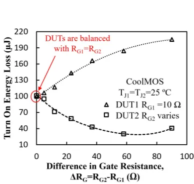
The measured switching energy is calculated by integrating the dissipated power (IDS·VDS) over the duration of the switching transients at turn-on and turn-off. Figure 5 shows the measured turn-on switching energy for the parallel connected SiC MOSFETs switched with different variations in switching rates i.e. RG2 – RG1 where RG2 is the gate resistance of DUT2 and RG1
is the gate resistance of DUT1. The switching rate of DUT1 is held constant with a gate resistance RG1=10 Ω while the
[image:3.595.311.543.56.218.2]switching rate of DUT2 is varied over a wide range of resistances. Figure 6 shows similar characteristics for the CoolMOS devices where the switching energies have been measured for each of the parallel DUTs switched at different rates. It is clear from Figure 5 and Figure 6 that not only do the SiC MOSFETs have smaller switching losses than the CoolMOS device but that the devices can cope with imbalances in the switching rates better. The maximum change in switching energies between the parallel connected DUTs is 40% higher for the CoolMOS devices under the same variation in switching
Fig. 1. Circuit schematic for the experimental set-up.
[image:3.595.308.548.249.416.2]rates i.e. ΔRG= RG2-RG1. It can also be seen that this variation in
switching energy (ΔESW) increases with the difference in
switching rate (ΔRG) for the CoolMOS while it is relatively
more stable for the SiC devices i.e. ΔESW/ΔRG is higher for the
CoolMOS than for the SiC device.
Figure 7 shows the measured turn-off switching energy for the parallel connected SiC MOSFETs while Figure 8 shows that of the CoolMOS devices. Unlike the turn-on characteristics shown in Figure 5 and Figure 6, the slower switching DUT exhibits higher switching energy. This is due to the current overshoots in the slower switching device during turn-off as shown in Figure 4. It can also be seen from Figure 7 and Figure
8 that ΔESW at a given ΔRG is smaller for SiC compared to the
CoolMOS device. This correlates well with Figure 4, where the current overshoot in the slower switching CoolMOS device is much higher than that in the SiC MOSFET.
Fig. 3. (a) Turn-on current waveforms for parallel connected SiC MOSFETs with different switching rates. (b) Similar characteristics for the CoolMOS device.
Fig. 4. (a) Turn-off current waveforms for parallel connected SiC MOSFETs with different switching rates. (b) Similar characteristics for the CoolMOS device.
Fig. 5. The measured turn-on switching energies of the parallel connected SiC MOSFET as a function of the difference in gate resistance.
[image:4.595.327.522.58.243.2]Fig. 6. The measured turn-on switching energies of the parallel connected CoolMOS devices as a function of the difference in gate resistance.
Fig. 7. The measured turn-off switching energies of the parallel connected SiC MOSFET as a function of the difference in gate resistance.
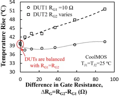
[image:4.595.326.521.285.441.2] [image:4.595.71.260.405.558.2] [image:4.595.326.521.483.639.2]The case temperatures have also been measured for each of the parallel DUTs so as to ascertain how the variation in switching rates (ΔRG) impacts the respective junction/case
temperatures of the individual DUTs. Due to the smaller die size in SiC MOSFETs, the junction-to-case thermal resistance for the SiC MOSFET is 1.8 °C/W while that of the CoolMOS device is 0.6 °C/W. Figure 9(a) shows the measured case temperature rise for the parallel connected SiC MOSFETs with repetitive switching at a frequency of 2 kHz with DUT1
switched at 10 Ω and DUT2 switched at 33 Ω. Figure 9(b) shows similar characteristics for the CoolMOS devices.
It can be seen in Figure 9 that the variation in the case temperature between the parallel connected DUTs is higher for the CoolMOS device than for the SiC MOSFETs. Figure 10 shows the measured steady state case temperatures for the parallel connected SiC MOSFETs repetitively switched at 2 kHz with different magnitudes of ΔRG=RG2-RG1. Figure 11
[image:5.595.47.290.206.312.2]shows the same plot for the CoolMOS device. By comparing Figure 10 and Figure 11, it can be seen that the SiC MOSFETs show less temperature variation (ΔTJ) between the respective
DUTs compared with the CoolMOS devices. Hence, the impact of mismatch in the switching rate of the parallel connected devices results in less temperature mismatch for the SiC MOSFETs compared with the CoolMOS devices. The smaller die sizes and less temperature sensitive electrical parameters in SiC mean that variations in temperature and switching rate between the parallel connected DUTs result in less mismatch in switching energy and dissipated power.
B. Impact of Initial Junction Temperature Mismatch
Similar measurements have been performed for parallel connected devices, however, with different initial junction temperatures. The initial junction temperatures are set by electric hot-plates connected to the base of the device. Since the system is at steady-state, it can be assumed that the case temperature is equal to the junction temperature. Figure 12(a) shows the turn-on current for the parallel connected SiC MOSFETs with different junction temperatures set by the heaters. Again, VDS=300 V. Figure 12(b) shows a similar plot for the CoolMOS devices. Figure 12 shows that the hotter device takes less current as expected because of the positive temperature coefficient of the on-state resistance and the current divider rule which stipulates that the more current flows through the more conductive device. By comparing the SiC and CoolMOS characteristics it can be seen that the steady state current mismatch is less for the SiC device compared with the CoolMOS device. This is due to the fact that SiC is more temperature resilient since its wide bandgap ensures that thermally generated carriers for any given temperature are smaller compared to those in silicon devices.
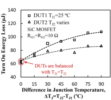
Figure 13 shows the measured turn-on energy of the parallel connected SiC MOSFETs with different magnitudes of initial
Fig. 9. (a) The measured case temperature rise for the parallel connected SiC MOSFETs switched with RG of DUT1 and DUT2 as 10 Ω and 33 Ω
[image:5.595.68.264.369.524.2]respectively. (b) Similar measurements for the CoolMOS device.
Fig. 10. The measured case temperature rise for the parallel connected SiC MOSFETs switched at different rates.
Fig. 11. The measured case temperature rise for the parallel connected CoolMOS devices switched at different rates.
[image:5.595.306.550.569.674.2] [image:5.595.70.265.570.727.2]junction temperature mismatch between the DUTs i.e. DUTs set at different ΔTJ =TJ2-TJ1 where TJ2 is the junction temperature of
DUT2 and TJ1 is the junction temperature of DUT1. In Figure
13, the junction temperature of DUT1 is held constant at 25 °C while the junction temperature of DUT2 is varied over a wide temperature range. Figure 14 shows similar characteristics for the CoolMOS device. It can be seen from Figure 13 and Figure 14 that the turn-on energy of the device at the higher junction temperature is lower. This is expected in MOSFETs because the turn-on dIDS/dt increases with temperature as a result of the
negative temperature coefficient of the MOSFET threshold voltage. It can also be seen by comparing Figure 13 with Figure 14 that the difference in turn-on energy loss (ΔESW) between the
parallel connected DUTs is smaller in SiC and remains more stable as ΔTJ is increased. Hence, it is demonstrated that parallel
connected SiC MOSFETs perform better than CoolMOS devices under both temperature and switching rate imbalances. As can be seen from the CoolMOS measurements in Figure 14, increasing the temperature difference (ΔTJ) between the parallel
DUTs results in much higher switching energy variation (ΔESW)
compared with the SiC MOSFETs.
IV. UNCLAMPED INDUCTIVE SWITCHING MEASUREMENTS
[image:6.595.332.523.90.262.2] [image:6.595.325.523.318.476.2]Under unclamped inductive switching (UIS), the device conducts current in avalanche mode. Avalanche mode conduction occurs when the electric field across the device exceeds the critical field, thereby causing carriers to accelerate, collide with atoms and generate additional electron-hole pairs if the collision energy exceeds the bandgap of the semiconductor. UIS measurements have also been performed on the parallel connected DUTs with mismatch in both the switching rate and initial junction temperatures. The goal was to determine the impact of mismatch between the parallel connected DUTs on the overall electrothermal robustness of the parallel pair. In UIS, the free-wheeling diode in parallel with the inductor is removed so that the inductor forces current through the parallel DUTs as they turn-off. The measurement set-up for UIS can be seen in [30, 31]. The size of the inductor determines the avalanche duration. As the parallel connected DUTs are forced into UIS, they will share current according to their breakdown voltages i.e. the device with the smaller breakdown voltage goes into avalanche. During UIS, the VDS rises to the breakdown voltage of the device. The initial conditions of the DUTs will impact the avalanche breakdown characteristics. The failure mode from UIS is parasitic BJT latch-up within the device which results from hole currents in the body causing a voltage drop between the source and p-body [32, 33]. Within a single device, non-uniformities between parallel conducting FET cells accelerates BJT latch-up. This is likewise the case between parallel conducting devices.
Figure 15(a) shows the avalanche current characteristics for each of the parallel connected SiC MOSFETs conducting current under UIS with different gate resistances. The supply voltage for the UIS measurements is 50 V. In Figure 15(a), DUT1 is driven by a 10 Ω gate resistance while DUT2 is driven by a 33 Ω gate resistance. Figure 15(b) shows similar characteristics for the parallel connected CoolMOS devices
driven with the same combination of mismatched gate resistances. It can be seen from both figures that the slower switching device fails under UIS. This is due to the fact that the slower switching DUT is still partially conducting at the time the avalanche current starts flowing. As a result the bulk of the avalanche current is forced through the slower switching DUT. Figure 16(a) shows the avalanche current characteristics for each of the parallel connected SiC MOSFETs conducting current under UIS with different initial junction temperatures. The junction temperature of DUT1 is set at 25 °C while that of DUT2 is set at 50 °C. Figure 16(b) shows the results of similar measurements performed on the CoolMOS devices. It can be seen from both plots in Figure 16 that the DUT with the initially lower temperature fails under UIS while that with the higher junction temperature does not. This results from the positive temperature coefficient of the breakdown voltage which means that the DUT with the higher initial junction temperature will have a higher breakdown voltage. This is due to increased
Fig. 13. Measured turn-on switching energy for the parallel connected SiC MOSFETs with the DUTs set at different junction temperatures.
phonon scattering reducing the carrier mean-free-path thereby delaying the on-set of sustained impact ionization that is necessary for avalanche mode conduction. Hence, the cooler DUT has a lower breakdown voltage and conducts all of the avalanche current which triggers the parasitic BJT and results in device failure. It can be seen from Figure 16 that the difference in the peak avalanche current between the parallel connected DUTs is higher for the CoolMOS than for the SiC MOSFET. This is due to the lower temperature coefficient of the on-state current in SiC compared to the CoolMOS device, hence, the imbalance in peak avalanche current between the parallel connected DUTs is lower in SiC than in CoolMOS.
The maximum avalanche current that the parallel connected DUTs are able to safely conduct (without thermal runaway) with a given mismatch in temperature and switching rate (ΔTJ and
ΔRG) has been determined for different avalanche durations and
for each device technology. This was done by increasing the duration of the gate pulse which in turn increases the current through the inductor and the peak avalanche current during UIS. It is known that the peak avalanche current that the DUTs can withstand without failure reduces as the avalanche duration increases since the total avalanche energy dissipated by the DUT is approximately equal to the energy stored in the inductor i.e. 0.5·LI2. Hence, as a larger inductor is used (avalanche
duration is increased), the peak current that the DUTs can safely conduct reduces and vice versa [31, 34]. It is expected that introducing mismatch (ΔTJ and ΔRG) in the parallel connected
DUTs will reduce the total peak avalanche current and energy sustainable by the parallel connected DUTs so the goal in these
[image:7.595.45.289.85.189.2]measurements is to quantify the reduction for the respective device technologies.
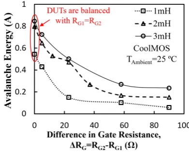
Figure 17 shows the peak avalanche energy sustained by the parallel connected SiC MOSFETs driven with different ΔRG
combinations. The UIS measurements have been performed with 3 different inductors which are used to set the avalanche duration. Figure 18 shows the same measurements performed on the CoolMOS devices. For both technologies, it is clear that increasing the switching rate mismatch (ΔRG) reduces the total
avalanche energy the parallel combination can withstand. This is for reasons explained in Figure 15 and Figure 16. However, what is also noticeable in Figure 17 and Figure 18 is that the rate at which the peak energy decreases with increasing ΔRG is much
higher for CoolMOS than for SiC. In other words, the parallel SiC MOSFETs are more avalanche rugged with increasing switching rate mismatch (ΔRG) than the CoolMOS devices.
Figure 19 shows the peak avalanche energy sustained by the parallel connected SiC MOSFETs driven with different ΔTJ
combinations. Figure 20 shows similar measurements for the CoolMOS devices. Similar to variations in the switching rate, the parallel connected SiC MOSFET perform better under temperature imbalance. Although the peak avalanche energy
Fig. 15. (a) Avalanche current characteristics for the parallel connected SiC MOSFETs with different RG. (b) Similar characteristics for CoolMOS.
[image:7.595.326.523.363.520.2]Fig. 16. (a) Avalanche current characteristics for the parallel connected SiC MOSFETs with different TJ. (b) Similar characteristics for CoolMOS.
Fig. 17. Peak avalanche energy in the parallel connected SiC MOSFETs for different ΔRG before failure under UIS.
[image:7.595.326.522.570.727.2]reduces with increasing temperature mismatch (ΔTJ) between
[image:8.595.316.536.57.230.2]the parallel connected DUTs, the reduction is quite small for the SiC MOSFETs compared with CoolMOS devices.
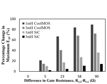
Figure 21 shows the comparison of the percentage change in the measured peak avalanche energy (EAV) for different ΔRG in
the parallel SiC and CoolMOS devices. It can be seen that the percentage change in the maximum avalanche energy is significantly smaller in the SiC MOSFETs than in the CoolMOS device. Figure 22 shows a similar plot, but with temperature variation between the parallel DUTs. Similar to the switching rate variation, the parallel connected SiC MOSFETs exhibit smaller variation in the avalanche characteristics.
Figure 23 shows the percentage change in the switching energy as a function of the variation in the switching rate (ΔRG).
The SiC MOSFETs perform better than the CoolMOS since the variation in the switching energy is less for a given magnitude of ΔRG between the parallel connected DUTs. A similar plot is
shown in Figure 24 for parallel connected devices set at different junction temperatures. Again, the percentage change in
the switching energy for a given ΔTJ is smaller for the SiC
[image:8.595.70.262.250.403.2]MOSFETs than for the CoolMOS devices.
[image:8.595.319.535.282.421.2]Fig. 19. Peak avalanche current in the parallel connected SiC MOSFETs for different ΔTJ before failure under UIS. 7
Fig. 20. Peak avalanche current in the parallel connected CoolMOS devices for different ΔTJ before failure under UIS.
Fig. 21. Percentage change in the peak avalanche energy (EAV) as a function of
[image:8.595.68.260.463.614.2]the switching rate difference between the parallel DUTs
Fig. 22. Percentage change in the peak avalanche energy (EAV) as a function of
the temperature difference between the parallel DUTs
Fig. 23. Percentage change in the turn-on switching energy (ESW) as a function
[image:8.595.327.522.483.632.2]V. FINITE ELEMENT SIMULATIONS
Finite element simulations have been performed in order to replicate the experimental measurements so as to understand the failure modes of parallel connected devices under UIS. The device simulations were done in SILVACO and the circuit simulations were performed using the mixed mode circuit application to solve the transient and steady-state circuit equations. The FET cells were simulated in parallel for both the SiC MOSFET and CoolMOS devices. The source n-type doping in the SiC MOSFET was set at 1×1019 cm-3 and the
p-body doping was 5×1017 cm-3. The doping of the deep p-body
implant was set at 1×1019 cm-3. The drift layer thickness was set
at 7 µm and the doping was set at 1×1016 cm-3. The channel
length was set at 1.9 µm and the cell area was 1.5 mm2. The
concentration dependent mobility model was used and the heat capacity and thermal conductivity were set as temperature dependent. In the case of the CoolMOS the p-pillar and n-drift region doping was balanced at 1×1015 cm-3 to have the
maximum breakdown voltage. Similar source and drain doping was used in the CoolMOS simulations. The oxide thickness for both devices was set at 50 nm. The lattice heating application package was activated to include electrothermal effects together with the appropriate impact ionization and temperature dependent mobility models.
Figure 25(a) shows the typical avalanche current characteristics for 2 parallel connected DUTs with equal and non-equal gate resistances. It can be seen that BJT latch-up occurs in the devices with RG1≠RG2 while it does not occur in the
devices with RG1=RG2. Figure 25(b) shows similar avalanche
current characteristics, however with the parallel connected DUTs set at different initial junction temperatures. Again, the device with TJ1=TJ2 does not undergo BJT latch-up while the
device with TJ1≠TJ2 does. Two-dimensional current density
contour plots have been extracted from the simulator at various points in time during the UIS characteristics. These have been labelled in Figure 25 as points X, Y and Z. The goal of these current density plots is to understand the internal current distribution within the devices during UIS for SiC MOSFETs and CoolMOS devices.
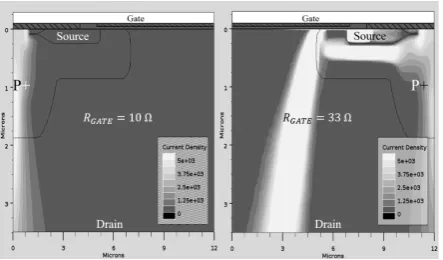
Figure 26 shows the 2-D current density contour plots of the parallel connected SiC MOSFETs at point X during the normal on-state conduction period of the UIS characteristics. It can be seen from Figure 26 that both DUTs conduct current normally prior to the on-set of avalanche. Figure 27 shows the 2-D current density contour plots at point Y (avalanche mode) for the parallel connected DUTs. It can be seen that the DUT with RG=10 Ω conducts the avalanche current through the deep
p-body that constitutes the internal body diode of the device. This region is usually doped with a high p+ concentration to ensure that the body is adequately shorted to the source in order to pre-empt the triggering of the parasitic BJT. However, it is evident from the current density contour plots of the DUT with RG=33 Ω, that there is significant lateral current through the
lightly doped p-body under the channel. This is due to the lower breakdown voltage since the slower switching device is not completely turned-off when the faster switching device abruptly diverts the current away i.e. at the instant when turn-off is initiated, the slower switching device has a lower breakdown voltage because it is not fully turned off.
Figure 28 shows the 2D current density contour plots for both DUTs at point Z corresponding to Figure 25(a), where it can be seen that the DUT with RG=10 Ω does not conduct any current
whereas that with RG=33 Ω is in full BJT latch-up i.e. the
[image:9.595.68.262.85.234.2]current flows through the npn BJT. This is in agreement with the experimental measurements shown in Figure 15(a).
Fig. 24. Percentage change in the turn-on switching energy (ESW) as a function
of the junction temperature difference (ΔTJ) between the parallel DUTs.
Fig. 25. (a)Simulated avalanche characteristics showing latch-up in parallel connected DUTs with RG1=RG2 and RG1≠RG2. (b) Similar characteristics with
TJ1=TJ2 and TJ1≠TJ2.
[image:9.595.305.549.88.200.2] [image:9.595.318.539.589.720.2]Similar characteristics are shown for the CoolMOS devices where Figure 29 shows the 2D current density contour plots at point X (conduction mode), Figure 30 shows the 2D plots at point Y (avalanche mode) and Figure 31 at point Z (BJT latch-up). The CoolMOS devices exhibit different latch-up characteristics than the SiC MOSFETs. By comparing Figure 31 to Figure 28, it can be seen that under BJT latch-up, the CoolMOS device exhibits more lateral currents due to presence of the p-pillar in the drift region.
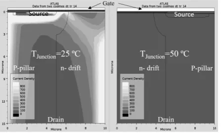
Figure 32 shows the 2D current density contour plots for the parallel SiC MOSFETs with different junction temperatures under UIS at point Z (in Figure 25(b)) where the devices are in latch-up. Figure 33 shows similar characteristics for the CoolMOS device. Similar to the experimental measurements in Figure 11, the DUTs with the lower junction temperature (TJ=25 °C) undergoes BJT latch-up due to its lower breakdown
voltage. This was confirmed by electric field plots showing higher fields in the device with the higher junction temperature. It can be seen that the avalanche current in the CoolMOS device has a significant lateral component while that in the SiC MOSFET is mostly vertical. The wider bandgap means that the temperature coefficient of the impact ionization rate in SiC is
[image:10.595.58.280.84.214.2]smaller compared to that in the silicon CoolMOS device Hence, variations in the junction temperature between the parallel DUTs cause less of a variation in the breakdown voltage in the SiC devices, therefore, the total avalanche energy sustainable by the parallel pair is less affected by variations in the initial junction temperature.
Fig. 27. 2D current density plots for parallel connected SiC with different gate resistances under UIS. This corresponds to point Y in Fig. 25(a) where the DUTs are under avalanche mode conduction.
Fig. 28. 2D current density plots for parallel connected SiC with different gate resistances under UIS. This corresponds to point Z in Fig. 25(a) where the slower switching DUT fails under BJT latch-up.
Fig. 29. 2D current density plots for parallel connected CoolMOS with different gate resistances under UIS. This corresponds to point X in Fig. 16(a) where the DUTs are under normal conduction mode.
Fig. 30. 2D current density plots for parallel connected CoolMOS with different gate resistances under UIS. This corresponds to point Y in Fig. 16(a) where the DUTs are in avalanche mode conduction.
[image:10.595.316.540.280.413.2] [image:10.595.57.280.283.412.2] [image:10.595.319.539.486.620.2]VI. CONCLUSIONS
In conclusion, it has been demonstrated that parallel connected SiC MOSFETs are more resilient to electrothermal imbalance than CoolMOS devices under both clamped and unclamped inductive switching. Given the same variations in switching rates and thermal resistance (junction temperature), SiC MOSFETs will exhibit less variations in the switching energy, steady state operating temperatures, maximum avalanche energy and output characteristics. This is due to lower switching losses (due to smaller parasitic capacitances) and less temperature sensitive electrical parameters.
REFERENCES
[1] F. Blaabjerg, M. Liserre, and M. Ke, "Power Electronics Converters for Wind Turbine Systems," IEEE Trans. Ind. Appl., vol. 48, pp. 708-719, Apr. 2012.
[2] J. Colmenares, D. Peftitsis, H. P. Nee, and J. Rabkowski, "Switching performance of parallel-connected power modules with SiC MOSFETs,"
in Int. Power Electron. Conf. (ECCE-ASIA), Hiroshima, Japan, May.
2014, pp. 3712-3717.
[3] D. P. Sadik, J. Colmenares, D. Peftitsis, L. Jang-Kwon, J. Rabkowski, and H. P. Nee, "Experimental investigations of static and transient
current sharing of parallel-connected silicon carbide MOSFETs," in 15th
Eur. Conf. Power Electron. Appl. (EPE), Sep. 2013, pp. 1-10.
[4] W. Xinke, C. Shidong, X. Qiang, and S. Kuang, "A 3600 V/80 A Series--Parallel-Connected Silicon Carbide MOSFETs Module With a Single External Gate Driver," IEEE Trans. Power Electronics, vol. 29, pp. 2296-2306, May. 2014.
[5] X. Qiang, Y. Yang, W. Xinke, R. Na, and S. Kuang, "A 10kV/200A SiC MOSFET module with series-parallel hybrid connection of 1200V/50A dies," in IEEE 27th Int. Symp Power Semiconductor Devices IC's
(ISPSD), Hong Kong, May. 2015, pp. 349-352.
[6] R. A. Wood and T. E. Salem, "Evaluation of a 1200-V, 800-A All-SiC Dual Module," IEEE Trans. Power Electronics, vol. 26, pp. 2504-2511, Sep. 2011.
[7] A. Sanchez-Ruiz, M. Mazuela, S. Alvarez, G. Abad, and I. Baraia, "Medium Voltage–High Power Converter Topologies Comparison Procedure, for a 6.6 kV Drive Application Using 4.5 kV IGBT Modules,"
IEEE Trans. Ind. Electron, vol. 59, pp. 1462-1476, Mar. 2012.
[8] V. Smet, F. Forest, J. J. Huselstein, F. Richardeau, Z. Khatir, S. Lefebvre,
and M. Berkani, "Ageing and Failure Modes of IGBT Modules in High-Temperature Power Cycling," IEEE Trans. Ind. Electron., vol. 58, pp. 4931-4941, Oct. 2011.
[9] O. Hyunseok, H. Bongtae, P. McCluskey, H. Changwoon, and B. D. Youn, "Physics-of-Failure, Condition Monitoring, and Prognostics of Insulated Gate Bipolar Transistor Modules: A Review," IEEE Trans.
Power Electron., vol. 30, pp. 2413-2426, May. 2015.
[10] J. Bing, S. Xueguan, C. Wenping, V. Pickert, H. Yihua, J. W. Mackersie,
and G. Pierce, "In Situ Diagnostics and Prognostics of Solder Fatigue in IGBT Modules for Electric Vehicle Drives," IEEE Trans. Power
Electron., vol. 30, pp. 1535-1543, Mar. 2015.
[11] V. Smet, F. Forest, J. Huselstein, A. Rashed, and F. Richardeau, "Evaluation of Vce Monitoring as a Real-Time Method to Estimate Aging
of Bond Wire-IGBT Modules Stressed by Power Cycling," IEEE Trans. Ind. Electron., vol. 60, pp. 2760-2770, Jul. 2013.
[12] O. Alatise, I. Kennedy, G. Petkos, and A. Koh, "Reliability of Repetitively Avalanched Wire-Bonded Low-Voltage Discrete Power Trench n-MOSFETs," IEEE Trans. Device and Mater. Rel., vol. 11, pp. 157-163, Mar. 2011.
[13] C. Ui-Min, F. Blaabjerg, and L. Kyo-Beum, "Study and Handling Methods of Power IGBT Module Failures in Power Electronic Converter Systems," IEEE Trans. Power Electron., vol. 30, pp. 2517-2533, May. 2015.
[14] S. Jahdi, O. Alatise, J. A. O. Gonzalez, R. Bonyadi, L. Ran, and P. Mawby, "Temperature and Switching Rate Dependence of Crosstalk in Si-IGBT and SiC Power Modules," IEEE Trans. Ind. Electron., vol. PP, pp. 1-1, Oct. 2015.
[15] X. Perpina, J. F. Serviere, J. Urresti-Ibanez, Corte, X. Jordan, S. Hidalgo, J. Rebollo, and M. Mermet-Guyennet, "Analysis of Clamped Inductive Turnoff Failure in Railway Traction IGBT Power Modules Under Overload Conditions," IEEE Trans. Ind. Electron., vol. 58, pp. 2706-2714, Jul. 2011.
[16] C. Nan, F. Chimento, M. Nawaz, and W. Liwei, "Dynamic Characterization of Parallel-Connected High-Power IGBT Modules,"
IEEE Trans. Ind. Appl., vol. 51, pp. 539-546, Jan. 2015.
[17] Z. Wang, X. Shi, L. Tolbert, F. Wang, Z. Liang, D. Costinett,and B. J.Blalock, "Temperature Dependent Short Circuit Capability of Silicon Carbide (SiC) Power MOSFETs," IEEE Trans. Power Electron., vol. PP, pp. 1-1, Sep. 2015.
[18] N. Thanh-That, A. Ahmed, T. V. Thang, and P. Joung-Hu, "Gate Oxide Reliability Issues of SiC MOSFETs Under Short-Circuit Operation,"
IEEE Trans. Power Electron., vol. 30, pp. 2445-2455, May. 2015.
[19] X. Zhuxian, X. Fan, and W. Fei, "Junction Temperature Measurement of IGBTs Using Short-Circuit Current as a Temperature-Sensitive Electrical Parameter for Converter Prototype Evaluation," IEEE Trans. Ind. Electron., vol. 62, pp. 3419-3429, Jun. 2015.
[image:11.595.56.281.89.221.2][20] X. Yang, L. Junjie, W. Zhiqiang, L. M. Tolbert, B. J. Blalock, and F. Wang, "Active current balancing for parallel-connected silicon carbide MOSFETs," in IEEE ECCE Conf., Denvor, USA., 2013, pp. 1563-1569. [21] O. Alatise, I. Kennedy, G. Petkos, K. Heppenstall, K. Khan, J. Parkin, A. Koh, and P. Rutter, "The Impact of Repetitive Unclamped Inductive Switching on the Electrical Parameters of Low-Voltage Trench Power nMOSFETs," IEEE Trans. Electron Devices, vol. 57, pp. 1651-1658, Jul. 2010.
Fig. 32. 2D current density plots for parallel connected SiC MOSFETs with different junction temperatures under UIS. Here, the cooler DUT fails in BJT latch-up.
[image:11.595.57.281.277.411.2][22] K. Fischer and K. Shenai, "Dynamics of power MOSFET switching under unclamped inductive loading conditions," IEEE Trans. Electron Devices, vol. 43, pp. 1007-1015, Jun. 1996.
[23] K. Fischer and K. Shenai, "Electrothermal effects during unclamped inductive switching (UIS) of power MOSFET's," IEEE Trans. Electron
Devices, vol. 44, pp. 874-878, May. 1997.
[24] J. McGloin and D. Sdrulla, "Estimating the temperature rise of power MOSFETs during the UIS test," in 17th Applied Power Electron. Conf.
and Expos. (APEC), Boston, USA., 1992, pp. 448-453.
[25] B. J. Daniel, C. D. Parikh, and M. B. Patil, "Modeling of the CoolMOSTM
transistor - Part I: Device physics," IEEE Trans. Electron Devices, vol. 49, pp. 916-922, May. 2002.
[26] C. Xing-Bi and J. K. O. Sin, "Optimization of the specific on-resistance of the COOLMOSTM," IEEE Trans. Electron Devices, vol. 48, pp.
344-348, Feb. 2001.
[27] Y. Wensong, Q. Hao, and L. Jih-Sheng, "Design of high-efficiency bidirectional DC-DC converter and high-precision efficiency measurement," in 34th IEEE Conf. IECON, Orlando, USA, Nov. 2008, pp. 685-690.
[28] J. S. Siva Prasad, R. Ghosh, and G. Narayanan, "Common-Mode Injection PWM for Parallel Converters," IEEE Trans. Ind. Electron., vol. 62, pp. 789-794, Feb. 2015.
[29] M. M. R. Ahmed and P. A. Mawby, "Analysis of parallel coolmos under saturation-mode operation," in 34th IEEE Conf. IECON, Orlando, USA, Nov. 2008, pp. 551-555.
[30] G. Breglio, A. Irace, E. Napoli, M. Riccio, and P. Spirito, "Experimental Detection and Numerical Validation of Different Failure Mechanisms in IGBTs During Unclamped Inductive Switching," IEEE Trans. Electron Devices, vol. 60, pp. 563-570, Feb. 2013.
[31] P. Alexakis, O. Alatise, J. Hu, L. Ran, and P. Mawby, "Improved Electrothermal Ruggedness in SiC MOSFETs Compared with Silicon IGBTs " IEEE Trans. Electron Devices, pp.2278-2286, Jul. 2014. [32] B. J. Baliga, Fundamentals of Power Semiconductor Devices, 1st ed.
New York, NY, USA: Springer-verlag, 2008.
[33] R. Bonyadi, O. Alatise, S. Jahdi, J. Hu, J. Ortiz Gonzalez, L. Ran, and P. Mawby, "Compact Electro-Thermal Reliability Modelling and Experimental Characterisation of Bipolar Latch-up in SiC and CoolMOS Power MOSFETs," IEEE Trans. Power Electron, vol. 30, pp. 6978-6992, Dec. 2015.
[34] D. L. Blackburn, "Power MOSFET failure revisited," in 19th IEEE
Power Electron. Spec. Conf., Kyoto, Japan, 1988, vol. 2, pp. 681-688.
Ji Hu (S’15) received the B.Sc. degree in electronic and electrical engineering from Northumbria University, Newcastle upon Tyne, U.K., in 2011, and the M.Sc. degree in energy and power electronics from the University of Warwick, Coventry, U.K., in 2013, where he is currently working towards the Ph.D. degree in power electronics. His interest in the field of power electronics and high power wide bandgap semiconductors led him to pursue his studies in the field of power electronics at the University of Warwick. His research interest is on the reliability and robustness of high voltage SiC power devices and finite-element device simulations. Mr. Hu is a Member of the IEEE Power Electronics Society.
Olawiwola Alatise received the B.Eng. degree (1st class honors) in electronic engineering and the Ph.D. degree in microelectronics and semiconductors from Newcastle University, U.K., in 2008. His research focused on mixed-signal performance enhancements in strained Si/SiGe metal–oxide–semiconductor field-effect transistors (MOSFETs). In June 2008, he joined the Innovation R&D Department, NXP Semiconductors, where he designed, processed, and qualified discrete power trench MOSFETs in switched-mode power supplies. Since August 2012, he is serving as Associate Professor of Electrical Engineering in University of Warwick, U.K. His research interest include advanced power semiconductor materials and devices.
Jose Angel Ortiz Gonzalez (S'15) received a degree in Electrical Engineering in 2009 from the University of Vigo, Vigo, Spain. From 2010 to 2012 he worked as a Support Technician at the Department of Electronics Technology, University of Vigo, Spain. Since 2013 he has been working at the School of Engineering, University of Warwick, Coventry, United Kingdom as a Power Electronics Research Associate while perusing a PhD degree in Power Electronics, currently focusing on condition monitoring, reliability and power cycling of high voltage Silicon Carbide based devices and circuits. His current research interests include power converters, circuits and device evaluation. Mr Gonzalez is a student member of the IEEE since 2015.
Petros Alexakis (S'12) received the BSc degree in Physics from Aristotle University in 2010 and the MSc degree with merit in Power Electronics from University of Warwick in 2012. He is currently pursuing his PhD in wide bandgap semiconductor devices in the University of Warwick. His research interests include modelling of wide bandgap semiconductor devices, reliability and ruggedness. Mr. Alexakis is a member of IEEE.
Li Ran (SM'07) received a PhD degree in Power Systems Engineering from Chongqing University, China, in 1989. He was a Research Associate with the Universities of Aberdeen, Nottingham and Heriot-Watt, at Aberdeen, Nottingham and Edinburgh in the UK respectively. He became a Lecturer in Power Electronics with Northumbria University, Newcastle upon Tyne in 1999 and was seconded to Alstom Power Conversion, UK in 2001. Between 2003 and 2012, he was with Durham University, UK. He joined the University of Warwick, UK as a Professor in Power Electronics - Systems in 2012. His research interests include the application of Power Electronics for electric power generation, delivery and utilisation.
![Fig. 2. This shows the picture of the experimental set-up with [1] Power Supply. [2] Test Chamber](https://thumb-us.123doks.com/thumbv2/123dok_us/9472610.453619/3.595.311.543.56.218/fig-shows-picture-experimental-power-supply-test-chamber.webp)