University of Warwick institutional repository: http://go.warwick.ac.uk/wrap
A Thesis Submitted for the Degree of PhD at the University of Warwick
http://go.warwick.ac.uk/wrap/53856
This thesis is made available online and is protected by original copyright.
Please scroll down to view the document itself.
JHG 05/2011
Library Declaration and Deposit Agreement
1. STUDENT DETAILS
Please complete the following:
Full name: ………. University ID number: ………
2. THESIS DEPOSIT
2.1 I understand that under my registration at the University, I am required to deposit my thesis with the University in BOTH hard copy and in digital format. The digital version should normally be saved as a single pdf file.
2.2 The hard copy will be housed in the University Library. The digital version will be deposited in the University’s Institutional Repository (WRAP). Unless otherwise indicated (see 2.3 below) this will be made openly accessible on the Internet and will be supplied to the British Library to be made available online via its Electronic Theses Online Service (EThOS) service.
[At present, theses submitted for a Master’s degree by Research (MA, MSc, LLM, MS or MMedSci) are not being deposited in WRAP and not being made available via EthOS. This may change in future.] 2.3 In exceptional circumstances, the Chair of the Board of Graduate Studies may grant permission for an embargo to be placed on public access to the hard copy thesis for a limited period. It is also possible to apply separately for an embargo on the digital version. (Further information is available in the Guide to Examinations for Higher Degrees by Research.)
2.4 If you are depositing a thesis for a Master’s degree by Research, please complete section (a) below. For all other research degrees, please complete both sections (a) and (b) below:
(a) Hard Copy
I hereby deposit a hard copy of my thesis in the University Library to be made publicly available to readers (please delete as appropriate) EITHER immediately OR after an embargo period of ………... months/years as agreed by the Chair of the Board of Graduate Studies.
I agree that my thesis may be photocopied. YES / NO (Please delete as appropriate) (b) Digital Copy
I hereby deposit a digital copy of my thesis to be held in WRAP and made available via EThOS. Please choose one of the following options:
EITHER My thesis can be made publicly available online. YES / NO (Please delete as appropriate) OR My thesis can be made publicly available only after…..[date] (Please give date)
YES / NO (Please delete as appropriate) OR My full thesis cannot be made publicly available online but I am submitting a separately identified additional, abridged version that can be made available online.
JHG 05/2011
Whether I deposit my Work personally or through an assistant or other agent, I agree to the following: Rights granted to the University of Warwick and the British Library and the user of the thesis through this agreement are non-exclusive. I retain all rights in the thesis in its present version or future versions. I agree that the institutional repository administrators and the British Library or their agents may, without changing content, digitise and migrate the thesis to any medium or format for the purpose of future preservation and accessibility.
4. DECLARATIONS
(a) I DECLARE THAT:
I am the author and owner of the copyright in the thesis and/or I have the authority of the authors and owners of the copyright in the thesis to make this agreement. Reproduction of any part of this thesis for teaching or in academic or other forms of publication is subject to the normal limitations on the use of copyrighted materials and to the proper and full acknowledgement of its source.
The digital version of the thesis I am supplying is the same version as the final, hard-bound copy submitted in completion of my degree, once any minor corrections have been completed.
I have exercised reasonable care to ensure that the thesis is original, and does not to the best of my knowledge break any UK law or other Intellectual Property Right, or contain any confidential material.
I understand that, through the medium of the Internet, files will be available to automated agents, and may be searched and copied by, for example, text mining and plagiarism detection software.
(b) IF I HAVE AGREED (in Section 2 above) TO MAKE MY THESIS PUBLICLY AVAILABLE DIGITALLY, I ALSO DECLARE THAT:
I grant the University of Warwick and the British Library a licence to make available on the Internet the thesis in digitised format through the Institutional Repository and through the British Library via the EThOS service.
If my thesis does include any substantial subsidiary material owned by third-party copyright holders, I have sought and obtained permission to include it in any version of my thesis available in digital format and that this permission encompasses the rights that I have granted to the University of Warwick and to the British Library.
5. LEGAL INFRINGEMENTS
I understand that neither the University of Warwick nor the British Library have any obligation to take legal action on behalf of myself, or other rights holders, in the event of infringement of intellectual property rights, breach of contract or of any other right, in the thesis.
Please sign this agreement and return it to the Graduate School Office when you submit your thesis.
Materials and Methods for Microstereolithography
by
Christopher Philip Purssell MEng (Hons)
Submitted in fulfilment of the requirements for the degree of Doctor of Philosophy
to the
University of Warwick
School of Engineering
i
Contents
List of Figures vi
List of Tables xiv
Acknowledgements xvi
Declaration xvii
Summary xviii
Abbreviations xx
1 Introduction 1
1.1 History of Manufacturing 1
1.2 Microfabrication 2
1.3 Microfabrication Methods 3
1.4 Additive Layer Manufacture 5
1.5 The ALM Process 6
1.6 ALM Methods 6
1.6.1 Solid Based Fabrication Methods 7
1.6.2 Powder Based Fabrication Methods 8
1.6.3 Liquid Based Fabrication Methods 9
1.7 Research Objectives 12
1.8 Thesis Outline 13
1.9 References 14
2 Microstereolithography 16
2.1 Introduction 16
2.2 Types of SL and MSL 18
2.2.1 Free Surface Systems 19
2.2.2 Two Photon / Dual Laser Stereolithography 21
ii
2.3.1 Digital Light Projection (DLP) Technology 31
2.3.2 Enhanced Resolution Modules (ERM) 34
2.4 System Operation 35
2.4.1 Design to Object Process 36
2.4.2 Post Processing 37
2.5 Microstereolithography Materials 38
2.5.1 Photopolymerisation Process 38
2.5.2 Material Overview 42
2.6 Considerations and Limitations 45
2.7 Conclusion 51
2.8 References 52
3 Custom Microstereolithography System Design 57
3.1 Introduction 57
3.2 Custom MSL System – Hardware 58
3.2.1 XYZ Stage 59
3.2.2 Arms 60
3.2.3 Build Platform 61
3.2.4 Resin Tray Stand 62
3.2.5 Resin Trays 63
3.2.6 Exposure Light Source 66
3.2.7 Dynamic Mask Generator 70
3.3 Custom MSL System – Software 72
3.4 Custom Multi-Material MSL System 75
3.5 Conclusion 80
3.6 References 81
4 Development of an MSL Compatible Magnetic Material 83
4.1 Introduction 83
iii
4.4 Initial Build Tests 93
4.4.1 Design and Fabrication 93
4.4.2 Testing 96
4.5 Multi-Layer Components 100
4.5.1 Fabrication of Multi-Layer Test Cubes 101
4.5.2 Mechanical Analysis 102
4.5.3 Poling and Field Detection 107
4.6 Conclusion 112
4.7 References 113
5 MSL for the Direct Fabrication of Flow Sensors 115
5.1 Introduction 116
5.2 Flow Sensors 117
5.2.1 Micro-Flow Measurement Techniques 118
5.2.2 Mechanical Flow Measurement Techniques 120
5.3 3D Printed Flow Sensors 125
5.3.1 2 Port Flow Sensor – Design 125
5.3.2 2 Port Flow Sensor – Fabrication 126
5.3.3 2 Port Flow Sensor – Testing 128
5.3.4 2 Port Flow Sensor – Results 131
5.3.5 Compact Lab-on-Chip Device Example – Design and Fabrication 134
5.3.6 Compact Lab-on-Chip Device Example – Testing 139
5.3.7 Compact Lab-on-Chip Device Example – Results 142
5.4 Conclusion 144
5.5 References 145
6 Development of an MSL Compatible Conductive Material 147
6.1 Introduction 148
6.2 Conductive Polymer Composites (CPCs) 149
iv
6.3.2 Carbon Black 159
6.4 Testing of the Material 165
6.4.1 Test Parts 165
6.4.2 Testing of Electrical Conductivity 167
6.4.3 Mechanical Testing 176
6.5 Conclusion 180
6.6 References 181
7 MSL for the Direct Fabrication of Vapour Sensors 183
7.1 Introduction 183
7.1.1 Analytical Based Detection 184
7.1.2 Sensor Based Detection 184
7.2 Conductive Polymer Sensors 187
7.3 Modification of the Conductive Composite Material 191
7.4 Device Design and Fabrication 192
7.4.1 Design 192
7.4.2 Fabrication 193
7.4.3 Mounting 194
7.4.4 Design improvement 196
7.5 Testing 200
7.5.1 Testing of I/V Linearity 203
7.5.2 Calculating Vapour Concentrations 206
7.5.3 Test Procedure 206
7.5.4 Results 209
7.6 Conclusion 218
7.7 References 220
8 Microstereolithography for Ultrasonic NDE Applications 225
8.1 Background 226
v
8.2.2 Calculating Parameters 235
8.3 CAD Design and Fabrication 238
8.4 Testing 243
8.4.1 Device Characterisation 243
8.4.2 Imaging Using the Focusing Device 247
8.5 Possible Improvements Using Alternative Materials 249
8.6 Conclusion 256
8.7 References 257
9 Conclusions and Further Work 259
9.1 Custom MSL System Design 260
9.2 Materials 262
9.2.1 Magnetic Material 262
9.2.2 Conductive Material 264
9.3 MSL for Ultrasonic NDE 266
9.4 Conclusions 267
9.5 Further Work 268
9.6 References 269
Appendix A 270
A Multi-Material Controller Schematic 270
Appendix B 271
vi
List of Figures
Figure 1.1 Diagram illustrating the design to fabricated component flow for additive layer technology processes 6
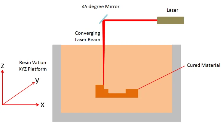
Figure 2.1 Diagram illustrating the stereolithography process of taking (a) a CAD model, (b) transferring it to a slicer program, and (c) dividing the model into representative slice images, such that the model can be (d) recreated as a physical component 16
Figure 2.2 Schematic diagram showing individual steps of a laser based, free surface stereolithography process. (a) 1 layer thickness is left between previously cured layer and surface of liquid material in resin vat, (b) a laser is used to photopolymerise the required pattern onto the surface of the resin material, (c) the build platform lower by 1 layer thickness, (d) the levelling arm recoats and levels the top surface of the material leaving a flat surface in preparation for the
following layer 20
Figure 2.3 A vial of fluorescent dye excited with NIR laser pulses demonstrating the selective curing of photopolymer in a 3D space (taken from Wu et
al) 22
Figure 2.4 Schematic diagram showing selective cutting method of two photon
microstereolithography 23
Figure 2.5 A model of the Sydney Opera House fabricated using two photon microstereolithography (taken from Wu et al) 24
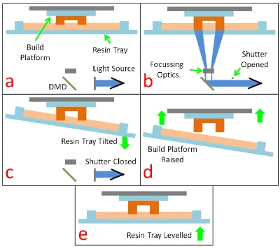
Figure 2.6 Schematic diagram showing process steps for fabrication using constrained surface microstereolithography with parallel dynamic mask projection. (a) a gap of 1 layer thickness is left between the previously cured layer and the bottom of the resin tray, (b) the image is set on the dynamic mask and the exposure shutter is opened; curing the resin, (c) the front edge of the resin tray is lowered to peel the newly cured layer from the resin tray, (d) the build platform is raised by 1 layer thickness, (e) the resin tray is re-levelled ready for
exposure of the following layer 26
Figure 2.7 A well micro structure fabricated using single mask parallel exposure method (taken from Nakamoto et al) 27
Figure 2.8 A mechanical gear printed using an LCD dynamic mask with laser exposure source and laser (taken from Bertsch et al) 29
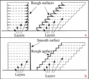
Figure 2.9 Diagram showing differences in surface finish from (a) laser / vector-by-vector and (b) parallel / dynamic mask methods of irradiation
(taken from Bertsch et al) 31
Figure 2.10 SEM micrograph of a the mirrors on a DMD 32
Figure 2.11 Schematic diagram illustrating the operation of a DMD based
projection system 33
vii
vinyl ether molecules 39
Figure 2.14 Chemical structure of Irgacure 369 40
Figure 2.15 Absorption profile for Irgacure 369 41
Figure 2.16 Spectral output of Perfactory Mini (EnvisionTec GmbH) 42
Figure 2.17 Ring designs for sacrificial casting fabricated using WIC and PIC
materials (EnvisionTec GmBH) 43
Figure 2.18 Illustration of fabrication error due components by either (a) the dimensions not being an integer number of voxels, or (b) the edge features not being collinear with the voxel matrix 46
Figure 2.19 Microscopy image of test build illustrating the failure of unsupported
overhanging features 47
Figure 2.20 Diagram showing the use of support structures to ensure the fabrication of otherwise unsupported features. (a) shows the intended component with an unsupported feature, (b) shows the same component with an additional support feature 48
Figure 2.21 Images showing (a) model vehicle with support structure, (b) a microfluidic component with surface deformities having removed the
support structure 49
Figure 2.22 Interference pattern observed when a laser spot is projected through a flat sample of material cured using a DMD based exposure 50
Figure 3.1 Photograph of custom microstereolithography system 59
Figure 3.2 CAD drawings of (a) left build platform support arm and (b) build platform clamp for custom MSL system (dimensions in mm) 61
Figure 3.3 Photograph of two build platforms manufactured for use with the custom MSL system, one (left) as a standard platform and a second (right) that includes a black backing to the glass build platform to prevent unwanted over cure when using un-dyed materials (scale
shown in cm) 62
Figure 3.4 CAD image of resin tray stand (left) and schematic drawing of resin tray platform for the custom MSL system (right) (dimensions in mm) 63
Figure 3.5 Photograph showing used commercial trays that have absorbed dye material in the exposure area therefore no longer of use in the
commercial EnvisionTec system 64
Figure 3.6 Custom resin plates cut from used EnvisionTec trays. The corner cuts are used to ensure the plates are used in the correct orientation. (scale
show in cm) 65
Figure 3.7 A photograph of (a) an Enfis Uno Air Light engine [8] and (b) the observed array pattern when focused and projected onto a surface 67
Figure 3.8 Spectral output of Enfis Uno Air 465nm light engine 69
viii
highlighted. (a) feedback for current motion stage position and light engine status, (b) manual controls for motion stage, (c) build platform calibration controls, (d) manual mask controls, (e) manual exposure controls, (f) build parameter override controls, (g) build pause control, and (h) current build status indicators 73
Figure 3.11 Photographic images showing test components fabricated using the custom MSL system ((a)-(d) and (f)), and an EnvisionTec Perfactory Mini system (e). (a) shows micro-impellers fabricated using a magnetic composite material. Other test components shown are a mug (b), three umbrellas ((c), (d) and (e)) and a set of cantilever beams (f). The orange material in (b), (d) and (e) is a commercial material (R11), the lighter material in (c) and (f) is a custom PEG based material developed specifically for the custom system. 74
Figure 3.12 Photographic images showing (a) carriage component of multi-material MSL system, (b) top and (c) reverse sides of resin tray
caddies 76
Figure 3.13 Photograph showing a HP Compaq MP1800 projector modified to use an Enfis Quattro Mini Air LED array for use in the multi-material
MSL system 77
Figure 3.14 Interface unit for controlling carriage motor and monitoring of sensors on the custom multi-material MSL system 78
Figure 3.15 Diagram showing the component parts of the custom multi-material
MSL system 79
Figure 3.16 A set of 6 example dog bone components fabricated using the
multi-material MSL system 80
Figure 4.1 Spin configurations for (a) paramagnetism, (b) ferromagnetism, (c) antiferromagnetism, (d) ferrimagnetism 86
Figure 4.2 Microscopy images of magnetite resin samples after (a) 5 minutes, (b) 10 minutes, (c) 15 minutes, and (d) 25 minutes of stirring 92
Figure 4.3 (a) CAD image (dimensions in mm) and (b) png of single layer for
comb device (dimensions in mm) 94
Figure 4.4 Microscopy image of comb device fabricated using magnetite
composite material (units in mm) 96
Figure 4.5 Photographic image showing test setup for measuring B-field effect of a permanent magnet on the magnetic comb test part (scale in cm) 97
Figure 4.6 Graph of displacement of fingers against magnet stand-off 99
Figure 4.7 (a) microscopy (scale in mm) and (b) SEM images showing filler voids in final layers of cube due to aggregation 100
Figure 4.8 (a) microscopy (scale in mm) and (b) SEM images showing successful build of cube with lower loading 101
Figure 4.9 Three cubes fabricated using magnetite composite material being attracted to a neodymium permanent magnet 102
Figure 4.10 Schematic showing direction of applied force for (a) along (parallel) plane and (b) through (perpendicular) plane compression testing
103
ix
Figure 4.12 Stress/strain graphs for compression tests of test cubes fabricated
with magnetite composite material 104
Figure 4.13 Stress/strain plot for R11 tensile test parts 105
Figure 4.14 Stress/strain plot for magnetite composite (25 µm layers) tensile test
parts 105
Figure 4.15 Stress/strain plot for magnetite composite (50 µm layers) tensile test
parts 106
Figure 4.16 Circuit diagram for the using the Honeywell HMC1001 AMR device for field detection of the magnetic composite material 108
Figure 4.17 Schematic diagram showing experimental setup used to map the B-field of the poled magnetite composite cube 109
Figure 4.18 Response of scanning AMR sensor over poled cube at increasing
standoff 110
Figure 4.19 Graph showing measured magnetic field strength of poled magnetite
cube over time 112
Figure 5.1 Example flow devices made in the MBL group (units in mm) (a) flow cell with observation window, (b) spiral micro-retentive column [4], (c) electroanalytical flow cell, (d) pneumatically drive micropump
[5], (e) DNA synthesis device 117
Figure 5.2 Schematic showing theory of operation of a float-type variable area
meter 121
Figure 5.3 Schematic showing theory of operation of a flap-type variable area
flow meter 122
Figure 5.4 Schematic showing theory of operation of a flow meter utilising a
magnetic turbine 123
Figure 5.5 Schematic showing theory of operation of a flow meter utilising a
magnetic impeller 124
Figure 5.6 CAD image and schematic of 2 port flow meter showing (a) the main body of the device, (b) the impeller, (c) the device’s lid 126
Figure 5.7 Photographic image of assembled flow meter (5 pence piece shown
for size reference) 128
Figure 5.8 Schematic of system setup for testing of 2 port flow meter 129
Figure 5.9 Photographic image showing experimental setup of the testing of 2 port flow meter. The input port of the device is connected to a regulated compressed air supply and the AMR sensing device is mounted above with the require amplifier circuit. 130
Figure 5.10 Measured signal from 2 port flow meter using AMR sensing device and an input pressure of 2 PSIG. 1 cycle per revolution. 132
Figure 5.11 Measured frequency with varying flow rate using 2 port flow meter 132
Figure 5.12 Suggested design improvement for MSL fabricated flow meters using rotating impellers
134
Figure 5.13 (a) CAD image and (b)schematic of 2 port flow meter (dimensions in
x
insufficient amount of superglue, (c) a viscous epoxy adhesive 137
Figure 5.15 Multi port micro flow meter with window (scale in mm) 138
Figure 5.16 Possible use of support material to enable device to be fabricated in a
single, multi-material process 138
Figure 5.17 Circuit diagram of amplifier with square wave output for direct frequency measurement of impeller rotation 140
Figure 5.18 Experimental setup for testing multi-port device 141
Figure 5.19 Observed relationship between measure flowrate and frequency of impeller rotation for multiport device 142
Figure 5.20 Measured signal from a single rotation of the 4mm diameter impeller 144
Figure 6.1 Particle distribution with (a) absolute minimum number of filler particles in order for conduction to occur, in an ideal situation, (b) absolute minimum number of filler particles in order for conduction to occur in a realistic situation, therefore no conduction due to the filler particles, (c) the realistic minimum number of particles in order to overcome the percolation threshold 150
Figure 6.2 10 µm Nickel particle distribution in PVC where the filler content is (a) less than the critical threshold, (b) equal to the critical threshold, (c) greater than the critical threshold (taken from Mamunya et al) 151
Figure 6.3 SEM image micrograph aggregation of Nickel nanoparticles due to
their ferromagnetic properties 154
Figure 6.4 SEM micrograph of (a) sieved and (b) excess copper particles 156
Figure 6.5 SEM micrograph of aggregated carbon black particles 161
Figure 6.6 Photographic image of resin material with filler of 10% by volume of carbon black using a monomer (HDDA) to cross-linker (DPPHA) in 3:1 ratio after 200 level peel cycles (5mm at 25µm layer thickness) at
(a) 1 mm/s, (b) 0.05 mm/s 162
Figure 6.7 Photographic image showing remains of failed components using 10%vol carbon black loading which became unattached from the build platform during fabrication do to too high peel speed 163
Figure 6.8 Patterns observed on build platform after using over-stirred carbon
composite material 165
Figure 6.9 CAD schematic of specimens for (a) tensile mechanical testing, (b) testing of electrical conductivity 166
Figure 6.10 Dynamic mask for fabrication process for test pieces generated by
slicer program 166
Figure 6.11 Photographic image illustrating method of testing (a) in plane resistance, (b) through plane resistance of test specimens (scale in
mm) 169
Figure 6.12 Photographic image showing glassy surface with numerous small indentations on bottom surface (final fabrication layer) of 10% vol carbon black specimen loaded square 170
Figure 6.13 Surface profile data from an interferometer scan of 10% vol loaded
xi
carbon black test specimen 171
Figure 6.15 Measured in plane conductivity of test specimens fabricated with a range of carbon black filler percentages 173
Figure 6.16 Measured through plane conductivity of test specimens fabricated with a range of carbon black filler percentages 174
Figure 6.17 Illustration of particle setting effect within layer structure 175
Figure 6.18 SEM micrograph of a sample with a 10% CB loading showing the
effects of particle settling 175
Figure 6.19 Measured ultimate tensile strength of PEG based test specimens fabricated with a range of carbon black filler percentages 176
Figure 6.20 Young’s Modulus of PEG based test specimens fabricated with a range of carbon black filler percentages 177
Figure 6.21 SEM micrographs of tensile test pieces with loadings of (a) 1.25%, (b) 2.5%, (c) 5%, (d) 7.5% and (e) 10% 178
Figure 6.22 SEM micrograph showing severe delamination caused by a combination of high loading (7.5%) and long exposure periods (180s) 179
Figure 7.1 Diagram of a chemoresistive gas sensor (for illustration only – not to
scale) 187
Figure 7.2 Simplified timing diagram illustrating the typical response profile of
a chemoresistive sensor 189
Figure 7.3 Schematic diagrams of version 1 vapour sensing devices in (a) standard and (b) slotted sensor geometries along with (c) side profile
(dimensions in mm) 193
Figure 7.4 Photographic images of (a) MSL fabricated vapour sensing devices on test stubs, (b) vapour test chamber 195
Figure 7.5 Schematic diagrams of version 2 vapour sensing devices in (a) standard and (b) slotted sensor geometries along with (c) side profile
(dimensions in mm) 198
Figure 7.6 Photographic image showing slotted version 2 vapour sensing
devices 199
Figure 7.7 Photographic image showing version 2 vapour sensing devices mounted onto test stubs. Image shows side view of a slotted device (left), top view of a slotted device (centre), and top view of a standard
device (right) 200
Figure 7.8 Schematic diagram of vapour test rig 201
Figure 7.9 Diagram of vapour senor device test circuit 202
Figure 7.10 Screenshot of interface and datalogging software for vapour sensing
devices 203
Figure 7.11 I/V plot for a slotted version 2 vapour sensor tested at range of temperatures
204
Figure 7.12 I/V plot for a slotted version 2 vapour sensor tested at range of temperatures. (data shown over a restricted range to illustrate small
xii
MSL fabricated vapour sensor with increase in ambient temperature 205
Figure 7.14 Timing diagram for vapour test rig 209
Figure 7.15 Unprocessed results from testing of selection of standard and slotted devices with ethanol and toluene sample vapours 210
Figure 7.16 Unprocessed results from testing of selection of standard and slotted devices with ethyl acetate and propan-2-ol 211
Figure 7.17 ∆R/R0 results from testing of selection of standard and slotted devices with sample vapours of ethanol at 1580 and 14830 ppm, toluene at 802 and 7690 ppm, ethyl acetate at 2860 and 26900 ppm, and propan-2ol at 1120 and 10560 ppm at 10%, 20% 30% and 50%
relative humidity 213
Figure 7.18 Response magnitude of 1 mm thick standard, solid MSL fabricated vapour sensing devices to ethanol, toluene, ethyl acetate and
propan-2-ol at a range of concentrations 215
Figure 7.19 Response magnitude of 1mm thick, slotted MSL fabricated vapour sensing devices to ethanol, toluene, ethyl acetate and propan-2-ol at a
range of concentrations 216
Figure 7.20 Magnitude response of MSL fabricated slotted vapour sensing devices to toluene at a range of temperatures and air humidity 217
Figure 7.21 Magnitude response of MSL fabricated slotted vapour sensing devices to ethyl acetate at a range of temperatures and air humidity 218
Figure 8.1 Diagram illustrating transmission and reflection of an incident wave normal to the interface with two medium 228
Figure 8.2 Schematic diagram of illustrating the principal of operation of a focusing device based on a Cassegrain reflector 229
Figure 8.3 Schematic diagram showing the key dimension of the design for the
focusing device 232
Figure 8.4 Plots of normalised axial pressure for transducers with circular elements with diameters of (a) 4, (b) 8, (c) 16, and (d) 32
wavelengths 234
Figure 8.5 Schematic diagram showing experimental setup for measurement of
transducer parameters 235
Figure 8.6 Line scan of the radial cross section of the unfocused transducer at an axial distance of 0.5mm from the transducer face 236
Figure 8.7 FFT measurement of the transducer’s nominal centre frequency 237
Figure 8.8 Graph showing normalised axial pressure plot showing (a) predicted normalised axial pressure amplitude, (b) the calculate near zone limit, (c) the specified geometric focus, and (d) the expected acoustic focal
length 238
Figure 8.9 Diagram illustrating the use of required support features if the focusing device were to be fabricated as one component. The circled regions highlight areas where the support structure would damage the
reflecting surfaces. 240
xiii
Figure 8.11 Microscopy image of the cross section of an MSL fabricated primary reflector using 50 µm layers with the continuous curved profile being approximated by a finite number of layers 242
Figure 8.12 Photographic images of (a) MSL fabricated component of focusing device, (b) assembled components mounted onto the end of the host
transducer 242
Figure 8.13 Schematic diagram showing experimental setup for characterisation
of focusing device 244
Figure 8.14 3D plot showing a sample measurement of the beam profile 245
Figure 8.15 Axial normalised pressure plots generated from initial design calculations and from maximum intensity measurements extracted
from plane scans 245
Figure 8.16 Plot showing beam profile at focal plane 246
Figure 8.17 Graph of radial line scan through focus maxima on focal plane 247
Figure 8.18 Schematic diagram showing experimental setup used for pulse echo mode imaging of a coin using transducer with focusing device 248
Figure 8.19 Plot showing an example of a typical recorded signal including responses generated from multiple reflections within the focusing
device 248
Figure 8.20 a) photographic image of UK 1p coin with additional plots generated from pulse echo scanning of (b) reverse and (c) front face using
transducer with focusing device 249
Figure 8.21 Schematic diagram showing experimental setup used for testing of acoustic properties or a range of MSL compatible materials 251
Figure 8.22 Graph showing speed of sound and acoustic impedance for the
sample MSL materials 252
xiv
List of Tables
Table 1.1 Comparison of different ALM technologies 10
Table 2.1 MSL systems presented by other researchers 18
Table 2.2 Comparison of key specifications between LCD and DMD based exposure systems (taken from Sun et al) 30
Table 2.3 Alternative photopolymer materials developed by other researchers 44
Table 3.1 Enfis Uno Air Specifications take from product datasheet 68
Table 4.1 Different types of magnetism 87
Table 4.2 Compressive yield strength of test cubes fabricated with magnetite composite and R11 materials with force applied both parallel and perpendicular to the fabricated layers 104
Table 4.3 Measured average tensile strength and Young’s modulus for R11, and
magnetite composite materials 106
Table 5.1 Fabrications settings for components of 2 port flow meter 127
Table 5.2 Fabrication settings for components of multi port flow sensor 136
Table 5.1 Fabrication peel and level velocity settings used for 100% to 250% copper composite materials depending on monomer used 157
Table 6.2 Fabrication settings used for 100% to 250% HDDA based copper
composite materials 157
Table 6.3 Fabrication settings and times for carbon composite materials with
various filler ratios 167
Table 7.1 Types of gas/vapour sensor technology 186
Table 7.2 Fabrication parameters for vapour sensor devices 194
Table 7.3 Characteristic of 3 MSL fabricated version 1 vapour sensing devices before and after adhesion to sample stubs 197
Table 7.4 Constants for Antoine’s Vapour Pressure Equation for toluene, propan-2-ol, ethanol and ethyl acetate 207
Table 7.5 Flow rate combinations used for testing of MSL fabricated vapour sensors to cover a range of humidity and sample vapour
concentration 208
Table 7.6 Calculated concentrations of sample vapours (to the nearest 10 ppm) 208
Table 7.7 Table of equations representing the responses of the two different device types to increases in relative humidity of the carrier air with
different sample concentrations 214
Table 7.8 Average sensitivity (from fractional response) for standard square sensors for the range of tested analyte vapours at varying relative humidity of carrier air (response/ppm *106) 219
Table 7.9 Average sensitivity (from fractional response) for slotted sensors for the range of tested analyte vapours at varying relative humidity of
carrier air (response/ppm *106) 220
xv
fabricated using MSL 241
Table 8.3 Physical properties of material samples tested for their acoustic
characteristics 251
Table 8.4 Measured acoustic properties from testing of a range of material
xvi
Acknowledgements
I would like to thank Dr. James Covington and Dr Duncan Billson for their support,
guidance and the lending of their invaluable expertise throughout the course of my PhD. I
would also like to acknowledge the EPSRC (Engineering and Physical Sciences Research
Council) for their funding.
I would like express my gratitude to my friend and colleague, Dr. Simon Leigh for
keeping the lab a lively place and for his guidance on all things chemistry related. Thanks
are also due to Frank Courtney, Ian Griffith and the rest of the technicians and support staff
whose knowledge and assistance is always greatly appreciated.
I would also like to thank all my other friends, family and colleagues, particularly,
Helen, Max, Matt, Phil, Charley and Fauzan for their support, encouragement and
willingness to lend a hand when needed. Also deserving of thanks are Allard, Nigel, Oli, Ali,
Louis, Kevin and the other metagrobologists for giving me an excuse to take a break every
once in a while.
xvii
Declaration
This thesis is presented in accordance with the regulations for the degree of Doctor
of Philosophy. The work described in this thesis is entirely original and my own, except
where stated otherwise. Parts of this work have been published in scientific journals and
presented at international conferences as listed below:
Journal Papers
C.P. Purssell, S.J. Leigh, M. Thomas, D.R. Billson, D.A. Hutchins, Microstereolithography for Fabrication of Devices for Ultrasonic NDE Applications, Ultrasonics (2012), Submitted for peer review.
S.J. Leigh, C.P. Purssell, J. Bowen, D.A. Hutchins, J.A. Covington, D.R. Billson, A miniature flow sensor fabricated by micro-stereolithography employing a magnetite/acrylic nanocomposite resin, Sensors and Actuators A: Physical 168 (2011) 66– 71.
S.J. Leigh, J. Bowen, C.P. Purssell, J.A. Covington, D.R. Billson and D.A. Hutchins, Rapid Manufacture of Monolithic Micro-Actuated Forceps Inspired by Echinoderm Pedicellariae, Bioinspiration & Biomimetics (2012), Bioinspiration & Biomimetics 7 (2012) 044001.
D. Cheneler, J. Bowen, S.J. Leigh, C.P. Purssell, D.R. Billson, D.A. Hutchins, M.C.L. Ward, Fabrication and analysis of cylindrical resin AFM microcantilevers, Ultramicroscopy 111 (2011) 1214–1223.
S.J. Leigh, R.J. Bradley, C.P. Purssell, D.R. Billson, D.A. Hutchins, A simple, low-cost conductive composite material for 3D printing of electronic sensors, PLoS ONE (2012), Submitted for peer review.
Conference Papers
xviii
Summary
There is an increasing requirement to fabricate ever smaller components and
micro-devices and incorporate them within all aspects of our lives. From a Wii controller to a car
airbag, micro-technology is employed in a huge spectrum of applications. Within process
control and sample analysis, micro-components are making a significant impact, driven by
the desire to use smaller volumes, lower concentrations, less reagent, or simply to make the
process quicker or cheaper. Currently, methods of fabrication for such devices are based
predominantly on silicon processing techniques. While these techniques are suitable for
mass manufacture / high volume applications, there are a number of disadvantages for
situations requiring lower volumes or where the end system is continually evolving – such as
for research applications. The primary drawbacks are cost, turnaround time and the
requirement for expensive processing facilities. However, for these situations, additive layer
manufacture presents huge promise as an alternative fabrication technology.
The field of additive layer manufacture has advanced greatly since its inception 25
years ago. While such technologies are still primarily focused on the field of rapid
prototyping of purely mechanical structures, it is clear that their full potential is yet to be
realised. This is particularly the case for stereolithography and microstereolithography, the
latter of which provides the capability to create complex, true 3D structures (as opposed to
pseudo 3D/extruded 2D of silicon techniques), measureable on the micron scale. This thesis
shows that microstereolithography has the potential to become an alternative fabrication
method for functional micro-devices and structures. This is due to the simplicity of its
single-step fabrication process and the significant time/cost savings it presents. Therefore,
making it an affordable technique for low volume production where a fast turnaround is
required. However, the lack of functional materials compatible with microstereolithography,
and hence the lack of examples of the technology being used to produce active components,
xix
microstereolithography as an alternative to traditional silicon based techniques for the direct
fabrication of functional micro-devices and sensors. This was achieved through the
development of a number of microstereolithography compatible, novel materials, methods
and applications. Here, presented for the first time are both conductive and magnetic
composite photopolymers compatible with microstereolithography technology. The
materials were developed with the use of a custom built, constrained surface system using a
parallel projection method. The system used LED technology as a novel exposure source,
tuned to the developed materials in an attempt to gain extra control over the curing process
and hence achieve higher quality components.
These materials were characterised and then used to fabricate exemplar sensing
devices using microstereolithography – a method not previously used for creating such
devices. Microfluidic flow sensing devices were used to demonstrate the practical
application of the magnetic material. One of which, a lab-on-chip type device, was
demonstrated to have a working range of 5 to 70 ml/min when tested with a liquid medium.
Similarly, a practical application of the conductive material was shown through the
fabrication of MSL-printed conductometirc vapour sensors. The sensors showed favourable
characteristics working in range of humidites (up to 50% RH) and temperatures (up to
70°C). The sensors also demonstrated a degree of selectivity to different analyte vapours.
Finally, the technology was demonstrated as a feasible method of fabricating ultrasonic
beam forming apparatus. Acoustic testing of a range of materials also suggested that the
composite metal materials could be used to further improve performance.
The novel materials and techniques investigated, along with the exemplar devices
produced, demonstrate further abilities and a wider range of applications than has been
demonstrated with this technology to date. It is hoped that this research will lead to wider
xx
Abbreviations
ABS - Acrylonitrile Butadiene Styrene
ADC - Analog to Digital Converter
ALM - Additive Layer Manufacture
ALT - Additive Layer Technology
AMR - Anisotropic Magneto-Resistive
API - Application Programming Interface
DLP - Digital Light Processing
DMD - Digital Mico-Mirror Device
DSP - Digital Signal Processing
FDM - Fused Deposition Modelling
GC - Gas Chromatography
GPIB - General Purpose Interface Bus
IC - Integrated Circuit
ICP - Intrinsically Conductive Polymer
LCD - Liquid Crystal Display
LED - Light Emitting Diode
MEMS - Microelectromechanical System
MS - Mass Spectrometry
MSL - Microstereolighography
NDE - Non-Destructive Evaluation
xxi RP - Rapid Prototyping
PCL - Poly Caprolactone
PLA - Poly (lactic acid)
PMMA - Poly (methyl methacrylate)
PNG - Portable Network Graphics
PTFE - Poly (tetrafluoro ethylene)
PVA - Poly (vinyl acetate)
PVP - Poly (vinyl pyrrolidone)
RFID - Radio-Frequency Identification
SFF - Solid Freeform Fabrication
SL - Stereolithography
STL - Standard Tessellation Language
USB - Universal Serial Bus
UV - Ultraviolet
1
Chapter 1
1
Introduction
Microstereolithography is an advanced fabrication technology capable of creating a
wide variety of micro-devices and structures. It is predominantly thought of as a rapid
prototyping technology. However, it has enormous potential as a manufacturing method, but
is currently held back due to a lack of functional materials and innovative examples of it
uses and methods.
This chapter begins by describing some existing manufacture and fabrication
methods. Next, an overview of additive layer manufacturing techniques and its advantages
are presented. The later sections detail the aims and objectives of the research undertaken.
Finally, there is a thesis outline detailing the contents of this thesis.
1.1
History of Manufacturing
Human’s ability to design and manufacture complex tools has been a major
distinction to the rest the animal kingdom. Archaeological research [1] has shown the use of
tools by humans as far back as the ~2.5 million years ago, with the first evidence of
manufacturing at ~1.76 million years ago, the “Acheulian”. Throughout the ages, man has
continued to discover new materials such as metals, and developed ways to utilise their
properties. A huge leap was made during the industrial revolution where there was a large
shift from manual labour to machine-based manufacturing. Ever since then, scientists and
engineers have been striving to push the boundaries of technology in order to make things
2
developments in recent time is the use of silicon and its associated technologies and
processes.
1.2
Microfabrication
There is a continuous drive in the fields of engineering and manufacture to produce
ever smaller and more compact devices and systems. This is particularly important in the
areas of biological synthesis, environmental monitoring and medical diagnosis. All of these
demand either smaller sample volumes or lower concentrations. Therefore, the main reasons
behind wanting to fabricate such micromechanical and microelectronic devices are to enable
the processing of increasingly smaller sample volumes, or use less reagent material. Either
of which can reduce running costs or increase the process speed. Indeed, this is also the
driving force behind lab-on-chip devices, which are able to provide increasingly more
integrated and compact solutions, that ultimately results in more efficient systems.
1.3
Microfabrication Methods
There are currently a variety of methods and techniques available to engineers to
fabricate components on virtually any scale. Traditional manufacture and machining
methods are generally forms of subtractive manufacture. This involves beginning the
fabrication process with one or more pieces bulk raw material and producing the desired
component by removing material from the bulk by drilling, milling, cutting, etc. The
removed material is considered as waste and is either disposed or recycled. While these
traditional machining techniques have been developed and adapted to increase precision and
resolution, the requirements for micromechanical and microelectronic devices tend to be
beyond the capabilities of such techniques. Fabrication of micro-devices and structures
3
This can be either for fabrication of the entire device or for one or more of the component
parts.
In general, the term “micromachining” is used to describe a method of creating
features on a substrate that can be measured in micrometres. The practice initially came
about through the microelectronics industry as a means of creating mechanical
microstructures such as beams, cantilevers, channels, springs etc either in, or on top of the
silicon substrate [2]. However, silicon micromachining is a multi-step, multi-process
fabrication technique, requiring a large range of expensive equipment, and depends almost
exclusively on the patterning and subsequent developing of a photoresist material on top of a
substrate.
The patterning is achieved through the use of a glass mask, selectively coated in a
light-blocking material (chromium is a common choice), which is itself created using a
lithography technique (by e-beam). Each mask can contain hundreds, even thousands of
component patterns. The mask is used to create the two dimensional patterns in the
photoresist, which is then developed. The developed photoresist is then used as a mask for
the next step of the process, for which there are two options. In the case of bulk
micromachining, the mask is used to define areas of the substrate to be etched. The etching
process can either be performed chemically (known as “wet etching”), or by a plasma
technique (known as “dry etching”). For surface micromachining, instead of modifying the
substrate, the mask is used to define area of the substrate where a secondary material it to be
deposited. These techniques can also be applied to other substrates too, such as ceramics.
Due to their widespread use in microelectronics, such silicon based fabrication
techniques are generally well understood, and are therefore often considered as the “go-to”
techniques for fabrication of micro-devices and structures. While such technologies are
clearly well suited to high volume / mass manufacture applications such as integrated circuit
4
volumes of devices are required, such as in a development or research environment, or
where the expected device lifetime is such that they can be considered disposable, such
processes still present a number of drawbacks.
Whether the fabrication is done in-house or externally, two of the major factors are
cost of production and turnaround time due to the (often complex) multi-step nature of the
process. Indeed the baking steps required for processing the resist can, on their own, take a
number of hours. If the fabrication were to be done in-house then there are added
considerations such as the requirement for expensive specialist equipment, handling of
corrosive chemicals, and again the cost in man-hours to oversee the process. Therefore, due
to the costs, and time involved in getting a design from idea to physical component it is
imperative that the design is correct first time. If the design needs modifying because it is
wrong or because it is unsuitable for the next iteration of the system design, then the process
must be started over again. This rapidly becomes an expensive route though, as the masks
alone can cost many hundreds of pounds to produce. These considerations can therefore
often make this approach financially prohibitive for small scale operations.
As such, it is therefore felt that for situations where a relatively low volume of such
functional micro-components are required at an affordable cost, an alternative method of
fabrication is required. However, one advantage silicon based processing has over other
technologies is the ability to create devices that have different functional layers (e.g.
conductive) and embedded functional components. Any alternate technology to silicon based
processing will be require to have the same functionality. It is, however, believed that a
5
1.4
Additive Layer Manufacture
Additive layer manufacturing techniques were initially developed as a rapid
prototyping technique, and are commonly used in a number of industries, the largest being
the automotive industry. In recent years, there has been increasing interest and development
in the use of these technologies (sometimes also referred to as solid freeform fabrication
(SFF) [3]). ALM is an interesting technology due its similarities with silicon technology (in
terms of its layer approach to fabrication) that could be applied to the production of parts,
but also offers a number of advantages over the use of silicon techniques. Initially, the most
obvious advantage is ALM’s ability to easily fabricate complex 3D structures. While this
can be achieved with silicon processes it is difficult to do and components are instead
restricted to having simple 2D geometry, or at best, a few superimposed layers.
In addition to not requiring expensive cleanroom facilities, the single-process, self
contained fabrication systems require minimal chemical materials which present
significantly less hazards that those of other micro-fabrication technologies. Due to the
nature of their single-process, fully automated method of fabrication, ALM technologies also
present a significantly more rapid method of manufacture (3-5 mm per hour), therefore
dramatically speeding up the turnaround time of components for an iterative development
process. While it could be argued that some ALM technologies require a certain amount of
post-processing, effectively making it a multi-step process, the time and equipment required
to perform these steps makes the argument largely irrelevant.
The main advantages of ALM over silicon based processing lie in the cost of the
production of components. This provides the design flexibility, which ultimately makes it a
far less financially prohibitive approach and enables the creation of components that are
tuned to specific applications. It is therefore felt that ALM presents great opportunities that,
6
1.5
The ALM Process
The ALM processes begins by using a computer aided design (CAD) package to
create a 3D model of the intended component(s). The 3D CAD model is then sliced into a
set of 2D cross-sections, each representing the component at a specific layer or z-height. The
2D cross-sections are then used by the ALM system to sequentially fabricate the layers one
on top of another. Figure 1.1 gives a basic illustration of the concept. Due to the nature of
the process, these fabrication methods usually generate little or no waste as material is only
added, rather than being removed.
Figure 1.1 – Diagram illustrating the design to fabricated component flow for additive layer
technology processes
1.6
ALM Methods
There is a wide variety of ALM systems currently available, each of which has its
own advantages and disadvantages for different applications. They cover systems that can
produce components ranging from headlight assemblies and toilet seats to microfluidic flow
cells. All ALM systems can be further classified under one of three groups, based on their
7
1.6.1 Solid Based Fabrication Methods
Solid based methods are those that use a pre-formed, solid, bulk material as the
primary method of fabrication. The two most notable methods solid-based systems are
laminated object manufacture (LOM) and fused deposition modelling (FDM).
LOM, or layered object manufacture (with other names such as Plastic Sheet Lamination
(PSL) and Paper Lamination Technology (PLT) given for more specific versions of the
technology), builds up the model layers by using laminar sheets of material. Each layer is
individually patterned using either a CO2 laser beam, steered using galvanic mirrors or a
blade. Before a layer is cut, adhesive is applied to the top of the previous layer so that the
layers of the model are bonded. In theory, any laminar sheet material can be used providing
it has a regular thickness and can be adhered. The excess material in the laminar sheets is not
removed during fabrication. This means that the method cannot be used to fabricate hollow
objects; however, the excess material is used as a support structure during fabrication. At the
end of the fabrication process the excess material needs to be manually removed. Typical
build resolutions for such systems are 100 µm in XY while the layer thickness is dependent
on the thickness of the laminate used; 100-200 µm is typical.
FDM systems create layers by vectoring the outline and infill space of the object using
an extruded thermoplastic material. A filament of the material (such as ABS, PLA
(polylactic acid), or PCL (polycaprolactone)) with greater diameter than the desired extruded
“string” is forced through a heated nozzle (usually between 150°C and 250°C depending on
the material), which is moved around the build area using an XY stage (sometimes the
extruder head is fixed and the build base is moved instead). Due to the means in which the
material is extruded they are also often colloquially called “toothpaste machines”. The
potential build envelope for FDM systems is only limited by the size of motion carriages that
hold the head, although dimensions on the order of 300 mm are typical. The resolution of
FDM systems is limited by the diameter of the extruded material; therefore, the resolution in
8
difficult to generate solid layers, as such, components fabricated using FDM have a degree
of porosity.
1.6.2 Powder Based Fabrication Methods
Powder based fabrication methods are some of the most commonly used in industry
due to self supporting nature of the fabrication process being able to produce large
components with uneven, undulating surfaces – such as prototypes for car headlight
assemblies. Selective laser sintering (SLS) and 3D printing (3DP) are the most common
example of the technology.
In order to create layers, SLS begins by spreading a thin layer of powdered material
(equal to one layer thickness) on top of the previous layer. A laser is then used to selectively
sinter the defined areas within each layer. The non-sintered material is left in the build area
and can therefore be used as a support structure. Similar methods which are derivatives of
SLS are electron beam melting (EBM), which uses an electron beam in place of a laser,
selective laser melting (SLM), which fills the fabrication chamber with an inert gas whilst
building, and selective mask sintering (SMS) which uses a parallel irradiation method and
masks that are generated by patterning toner onto a glass plate. The resolution of SLS
systems is on the order of 0.5 mm.
In a similar manner to SLS, 3DP constructs each layer by spreading a layer of the
powdered material on top of the previous. However, instead of melting or sintering the
material, a print head (similar to those found in ink-jet printers) deposits a binding material
onto the powder surface. The binder can also include inks that allow full colour models to be
generated in one fabrication process. The resolution of such systems can be down to around
9
1.6.3 Liquid Based Fabrication Methods
Liquid based fabrication methods are those that rely on the solidification of a
photosensitive liquid polymer. There are a number of systems that use this principle to
fabricate components, the most well-known of these is stereolithography apparatus (SLA).
SLA is generally considered as being one of the first, if not the first, method of ALM. The
earliest reference found was from a paper published in 1981 by Hideo Kodama [4] where the
process was first outlined. Six years later, in 1987, 3D Systems (USA) produced the first
commercial system [2, 5].
Traditional SLA systems operate by positioning a flat build platform in a vat of resin
material such that one layer thickness material remains between the free surface of the
material and the previously solidified layers. The layer is created by selectively manipulating
light in order to polymerise a photocurable liquid polymer resin into a solid polymer in the
desired pattern. This can achieved either by using galvanic mirrors to steer a laser beam (UV
[6] or IR [7]), by employing a dynamic mask system [8]. Once the material is cured, it
remains solid and will not re-dissolve in the monomer [9]. SL systems can achieve layer
thicknesses of 100 µm with XY resolutions of 50 µm. Microstereolithography (MSL or µSL)
is a form of SL that can be used to fabricate parts on the micron scale and therefore presents
a possible alternative to silicon based fabrication methods. Depending on the system, layer
thicknesses of 20 µm can be achieved with an XY resolution also down to 15 µm. The
process is discussed in greater detail in the following chapter.
There is a further liquid based method, rather confusingly also referred to as 3D printing.
This method again uses ink-jet technology to deposit measured amounts of material in the
desired 2D pattern for each layer. The material is then immediately cured using a UV light
source, which is attached to the print head. The systems employing this technology can have
large build envelopes - up to 490mm x 390mm x 200 mm for the Eden 500v (Objet Ltd,
10
11
Table 1.1 shows a comparison of systems, a number of which show promise as a
potential solution to the issue of affordable fabrication of functional devices. However, it is
felt that stereolithography and in particular, microstereolithography, show particular promise
as an alternative method to fabricate functional devices and components with
micro-structures. The use of its micro-scale manufacturing capabilities have already been
demonstrated through its use in the jewellery industry for creating moulds for the casting of
rings etc. However, commercial system manufacturers appear to be content with this, and
the current range materials and methods limit its use to purely structural or mechanical
components. Therefore there are a great number of materials covering these applications,
some including ceramics/glass particles for increased strength, others being wax based
aimed at casting applications.
The combination of advantages that MSL has over other ALM technologies,
specifically its resolution combined with the ability to use low material volumes and
incorporate secondary, possible functional components within the material (as demonstrated
by the commercially available ceramic materials), make it ideal as an alternative to silicon
processing. While some researchers have begun to demonstrate the potential uses of MSL in
more engineering related applications, such as basic air coupled ultrasonic transducers [10,
11] and micro-mechanical bellows [12], it is difficult to find any that present the material
itself providing functional significance in an application. One exception to this is where
researchers have begun to explore its uses in the medical field, for generation of bone and
tissue scaffolds [13-18]. As such, there is a need to expand the range of available materials
through the development of novel, functional materials. By increasing the range of materials
to include those with additional functional properties, introducing new ideas for methods of
fabricating existing components, and creating additional exemplar components using this
technology, it is felt that the advantages of MSL could become more clearly seen. It is felt
12
an invaluable future technology as a possible alternative to more traditional techniques of
micro-manufacture.
1.7
Research Objectives
The recent advances of microstereolithography techniques (discussed further in
Chapter 2) have bought the technology to a point where micro-mechanical structures can be
fabricated with relative ease. However, to date, research has focused primarily on
improvements in resolution and the fabrication of structural components, thus there is a great
need for development in materials and their uses in order to expand the applications of the
technology.
The aims of this work are therefore to attempt to overcome some of the current
limitations of the technology by exploring the envelope of possibilities for MSL such that
the potential uses of microstereolithography covers a wider range of applications. This will
be done through the development of a number of microstereolithography compatible, novel
functional materials and methods to find out what is achievable. This project will also aim to
demonstrate potential applications of microstereolithography through the fabrication of
exemplar functional devices.
Investigations will be carried out into the feasibility of creating both composite
magnetic and conductive materials compatible for use in MSL apparatus. The potential of
using microstereolithography to fabricate functional micro-devices using the new material
will be examined through the design and fabrication of exemplar microfluidic flow and
chemoresistive vapour sensing devices. Additionally, the use of microstereolithography for
the fabrication of ultrasonic devices for use in non-destructive evaluation applications will
13
then be compared to that of commercial materials in an attempt to identify methods of
increasing performance.
It is hoped that the research conducted in this thesis will increase the capabilities,
scope and awareness of microstereolithography technologies, such that it widens the range
of possible applications and enables an increase of its future use for the affordable, direct,
rapid manufacture of a greater range of functional micro-devices and sensors.
1.8
Thesis Outline
Chapter 2 covers in greater depth the different variants of microstereolithography systems, including the specific steps involved in the fabrication process and the curing
mechanism of the materials. There is a particular focus on constrained surface systems using
parallel exposure methods. A number of limitations of the technology along with points that
should be considered when attempting to fabricate using MSL are also covered, along with
example structures.
Chapter 3 details the design and manufacture of two custom microstereolithography systems. Developed as part of this project, they employed LED
technology as an exposure source, with the second system focused on the fabrication of
multi-material component fabrication. The systems developed were used in the later sections
of this work.
Chapter 4 discusses the development and testing of a novel photocurable magnetic composite material for use in the development of 3D printed sensors and micro-actuators.
This chapter also describes mechanical testing as well as investigating the new material’s
response to an applied magnetic field. A method of detecting the material’s magnetic field

![Figure 2.10 – SEM micrograph of a the mirrors on a DMD [39]](https://thumb-us.123doks.com/thumbv2/123dok_us/9652410.467250/57.595.182.459.71.275/figure-sem-micrograph-mirrors-dmd.webp)