warwick.ac.uk/lib-publications
A Thesis Submitted for the Degree of PhD at the University of Warwick
Permanent WRAP URL:
http://wrap.warwick.ac.uk/80601
Copyright and reuse:
This thesis is made available online and is protected by original copyright. Please scroll down to view the document itself.
Please refer to the repository record for this item for information to help you to cite it. Our policy information is available from the repository home page.
iii
The Development and Optimization of Potential Germanium
on Silicon Single Photon Avalanche Diodes
by
Philip Simon Allred
Submitted to the University of Warwick
in partial fulfilment of the requirements
for admission to the degree of
Doctor of Philosophy
Declaration
This thesis is submitted to the University of Warwick in support of my application for the degree of Doctor of Philosophy. All experimental work presented was carried out by the author, or (where stated) by specialists under the author’s direction.
v Acknowledgments
The work in this thesis would not have been completed without the help, guidance and patience of my supervisors, Prof. David Leadley and Dr. Maksym Myronov. I am very grateful to Dr Maksym Myronov for the proposal, design and epitaxy of Si and Ge based materials by RP-CVD. Also for providing encouragement and plenty of samples to keep me busy, as well as sharing an appreciation for mixed grills.
I would like to thank all the members of the nano Silicon group throughout my time. I owe both Vishal Shah and Stephen Rhead enormous thanks for sharing some of their wisdom. I am grateful for the current members; Olly for pushing my lungs to new limits but being inferior in the weight room, Jamie for the perfect geoguesser distractions (1.6m), Turbo for his chemistry knowledge and vehicular assistance, Dave for the extra curriculars, Gerard for help during the membrane process, and vineet. I would like to thank previous members James, John for help with the TEM, and Cat for the frequent cakes.
I must thank Ind massively for putting up with me for so long. He was able to provide some much needed distractions when they were necessary. I am also very grateful for the support of Stephen Ball throughout, but particularly in the latter stages with some extra gym sessions.
I would also like to thank someone who gave me an immeasurable amount of support through part of my PhD. They may not have realised the significance of her help. But they were there to give me focus through some of the stressful periods, as well as give me some unforgettable experiences. They believed in me at times when perhaps I didn't. I can't thank them enough for the part they played, I was very lucky. I would also like to include their family in these acknowledgements too, as they were very kind to me also. For that I am truly grateful.
Special thanks go to Ally Caldecote, who was there to pick me up during what has proved to be the toughest period of my life. Without the generous supplies of chicken and salmon, and the patience to listen to me, there wouldn't be a thesis to read. She has been there for me when I have really needed.
I would like to thank my friends from home including Pierre Taylor, Rob Tambini, Alex Pope, Adam Lloyd, Edward Vernon, Milky, Sam Rest, and Paul Ramsay. They kept me entertained throughout. Huge thanks go to my family, who have had to see me at my worst. A lot of credit goes to them for getting me to this stage in the first place. While things have been far from smooth at points I don't know where I would be without the help and support I have had.
vi
Abstract
vii
Publications and Presentations
Papers
1. P. Allred, S.D. Rhead, M. Myronov, R.E. Warburton, G. Intermite, G.S. Buller,
D.R. Leadley,
Epitaxial growth challenges of thick Ge-on-Si structures used for single photon
avalanche diode applications, In Preparation
2. P. Allred, S.D. Rhead, M. Myronov, D.R. Leadley,
Suspended SiB structures grown using RP-CVD for application to Group IV Single
Photon Avalanche Diodes, In Prepartaion
3. V.A. Shah, S.D. Rhead, J. Finch, M. Myronov, J.S. Reparaz, R.J. Morris, N.R.
Wilson, V. Kachkanov, I.P. Dolbnya, J.E. Halpin, D. Patchett, P. Allred, G.
Colston, K.J.S. Sawhney, C.M. Sotomayor Torres, D.R. Leadley
Electrical properties and strain distribution of Ge suspended structures
Solid State Electronics 108, 13, (2015)
4. S.D. Rhead, J.E. Halpin, V.A. Shah, M. Myronov, D.H. Patchett, P.S. Allred, V.
Kachkanov, I.P. Dolbnya, J.S. Reparaz, N.R. Wilson, C. M. Sotomayor Torres and
D.R. Leadley
Tensile Strain Mapping in Flat Germanium Membranes
viii
5. V.A. Shah, S. Rhead, J Halpin, O. Trushkevych, E. Chávez-Ángel, M. Myronov,
J.S. Reparaz, R. Edwards, F. Alzina, A. Shchepetov, S. Kachkanov, N. R. Wilson,
I. Dolbnya, D.H. Patchett, P.S. Allred, M.J. Prest, P.M. Gammon, M. Prunnila,
T.E.Whall, E.H.C. Parker, C.M. Sotomayor Torres, D.R. Leadley
High Quality Single Crystal Ge Nano-Membranes for Opto-Electronic Integrated
Circuitry
Journal of Applied Physics 115, 144307 (2014) DOI: 10.1063/1.4870807
6. R.E. Warburton, G. Intermite, M. Myronov, P. Allred, D.R. Leadley, K. Gallagher,
D. J. Paul, N. J. Pilgrim, L.J.M. Lever, Z. Ikonic, R.W. Kelsall, and G.S. Buller
Ge-on-Si single photon avalanche diode detectors: Design, modeling, fabrication,
and characterization at 1310 and 1550 nm
IEEE Transactions on Electron Devices, 60, 2282712 (2013)
Conference Presentations
1. Van Huy Nguyen, M. Myronov, P. Allred, J. Halpin A. Dobbie and D.R.
Leadley
Developments in Germanium-on-Silicon epitaxy by reduced pressure chemical
vapour deposition
ULIS 2014, Stockholm, Sweden, April 2014
2. S.D. Rhead, J.E. Halpin, V.A. Shah, M. Myronov, D.H. Patchett, P.S. Allred, V.
Kachkanov, I.P. Dolbnya, N.R. Wilson and D.R. Leadley
Tensile Strain Mapping in Flat Germanium Membranes
7th Intl. Silicon-Germanium Technology and Device Meeting (ISTDM) Singapore,
ix
3. P.S. Allred, M. Myronov, S.D. Rhead, R. Warburton, G. Intermite, G. Buller
and D.R. Leadley
Optimization of Epitaxial Growth for Thick Ge-on-Si Structures used for Single
Photon Avalanche Diode Applications
7th Intl. Silicon-Germanium Technology and Device Meeting (ISTDM) Singapore,
June (2014)
4. M. Myronov, J. Halpin, S. Rhead, Van Huy Nguyen, D. Patchett, P. Allred, J.
Foronda, V. Shah, C. Morrison, G. Colston, V. Sivadasan, D.R. Leadley
Silicon-based epitaxy capability at the University of Warwick
UK Silicon Photonics Conference, Southampton, Nov. 2013
5. P. Allred, M. Myronov R. Warburton, G. Intermite, K. Gallacher, N. Pilgrim, L.
Lever, D.J. Paul, Z. Ikonic, R. Kelsall, G. Buller and D.R. Leadley
Development of Ge-on-Si Single-Photon Avalanche Diodes.
UK Silicon Photonics Conference, Southampton, Nov. 2013
6. G. Intermite, R.E. Warburton, M. Myronov, P. Allred, D.R. Leadley, K.
Gallagher, D.J. Paul, N.J. Pilgrim, L.J.M. Lever, Z. Ikonic, R.W. Kelsall, and G.S.
Buller
Design and performance of a prototype mesa-geometry Ge-on-Si single-photon
avalanche diode detector at 1310 nm and 1550 nm wavelengths
Group IV Photonics, Seoul, August 2013
7. O.A. Mironov, A.H.A. Hassan, A. Dobbie, R.J.H. Morris, A. Feher, E. Cizmar,
S. Gabani, I.B. Berkutov, J.E. Halpin, S.D. Rhead, P. Allred, and D.R. Leadley
x QWs on (100)Si as basis material for post-Si CMOS technology
E-MRS Spring Meeting, Strasburg, May 2013
Glossary of terms
AFM – Atomic force microscope
APD – Avalanche photodiode
CCC – Closed cycle cryostat
CCD – Charge coupled device
CRL – Compound refractive lens
CVD – Chemical vapour deposition
DCR – Dark count rate
FTIR – Fourier transform infrared spectrometry
GS-MBE – Gas source molecular beam epitaxy
HF – Hydrofluoric acid
HH – Heavy hole
IR – Infrared
LH – Light hole
MBE – Molecular beam epitaxy
MOSFET – Metal oxide semiconductor field effect transistor
NEP – Noise equivalent power
PMT – Photomultiplier tube
RP-CVD – Reduced pressure chemical vapour deposition
RSM – Reciprocal space map
SAM – Separate absorption and multiplication
SEM – Scanning electron microscope
SIMS – Secondary ion mass spectrometry
SOI – Silicon on insulator
SPAD – Single photon avalanche diode
xi
SS-MBE – Solid source molecular beam epitaxy
TDD – Threading dislocation density
TEM – Transmission electron microscope
TMAH – Tetramethylammonium hydroxide
UHV-CVD – Ultra high vacuum chemical vapour deposition
VdP – Van der pauw
XRD – X-ray diffraction
𝜇 - mobility
𝛼 – absorption coefficient/electron impact ionization coefficient
𝛽 - hole impact ionization coefficient
ρ - resistivity
θ – theta angle
𝜔 – omega angle
F – excess noise factor
M – multiplication gain
Eg – Band gap
𝜆 – wavelength
qx – in plane reciprocal lattice vector
qz – out of plane reciprocal lattice vector
VH – Hall voltage
xii
Table of Contents
User’s Declaration i
Title Page iii
Declaration iv
Acknowledgments v
Abstract vi
Publications and Presentations vii
Glossary of terms x
Table of Contents xii
List of Figures xvi
1. Introduction to Si and Ge
1.1 The Semiconductor industry 2
1.2 Photon-detection 3
1.3 Summary 4
2. Background Theory
2.1 Basic Properties of Si and Ge 7
2.2 Strain enhancement 8
2.3 Doping semiconductors 11
2.3.1 Dopant Migration via diffusion and segregation 16 2.3.2 High Doping Concentrations 17
2.4 pn junctions 18
2.4.1 Biasing pn junctions 20
2.5 Single Photon Avalanche Diodes 21
2.5.1 Dark Counts 26
xiii
2.6 Photolithography Processes 35
2.7 Suspended Membranes and Wire 37
2.7.1 Etching 37
2.7.2 Membrane etching 38
2.7.3 Suspended works 38
3. Experimental Techniques
3.1 Transmission electron microscopy 43
3.1.1 TEM sample preparation 47
3.2 Atomic force microscopy 48
3.3 X-ray diffraction 50
3.3.1 X-ray measurements using synchrotron radiation 58
3.3.2 (004) RSM with micro-focus diffraction 61
3.4 Hall effect measurements 63
3.5 Growth techniques 66
3.5.1 Precursor gases and growth modes 66
3.5.2 Growth kinetics 70
3.5.3 Substrate preparation 70
3.5.4 Reduced pressure CVD 71
3.6 Secondary ion mass spectrometry 72
4. Development of Ge on Si Epitaxial SPAD device
4.1 Single Photon Avalanche Diodes 76
4.2 Optimization of absorption and multiplication regions 76
4.2.1 Growth of Silicon multiplication region 77
4.2.2 Growth of Germanium multiplication region 79
4.3 Optimization of doped layers 84
4.3.1 Segregation in the layers 85
xiv
4.3.3 Reduced temperature and multiple LT/HT steps 91
4.3.4 Doping concentrations for SAM SPAD device 95
4.4 Single photon avalanche diode designs using Si and Ge 98
4.4.1 Pure Silicon SPAD design 98
4.4.2 Pure Germanium SPAD design 101
4.4.3 Summary of Si SPAD and Ge SPAD 104
4.4.4 Ge and Si SAM SPAD 104
4.4.5 Charge sheet doping concentration 108
4.4.6 New pipin Si and Ge SAM SPAD 109
4.4.7 Replacement of doped substrate with SiP epilayer 118
4.5 Electrical characteristics of SPAD device 122
4.5.1 Dark current measurements for sample 13-191 124
4.5.2 Dark current measurements for sample 14-329 128
4.6 Single photon detection for SPAD sample 13-312 133
4.7 SPAD Summary 137
4.8 Suspended SPAD device concept 140
5. Very Low Resistance Ohmic Contacts for SPAD Device
5.1 Motivation for highly doped SiB layers 143
5.2 Growth of highly doped SiB layers 145
5.3 Structural characterization of SiB Layers 148
5.3.1 Dopant concentration calculations from XRD 154
5.4 Electrical characterization of SiB layers 157
5.4.1 Dopant concentration calculations from VdP 158
5.5 SiB Bulk structural and electrical summary 160
6. Suspended Membrane and Wires
6.1 Development of membranes and wires 166
xv
6.2 Optimization of fabrication processes 168
6.2.1 Membrane fabrication 169
6.2.2 Wires fabrication 171
6.3 Synchrotron measurements 172
6.3.1 Analysis of suspended SiB membrane 172
6.3.2 Analysis of suspended SiB wires 173
6.4 Summary of SiB wires and membrane 179
6.4.1 Corner characteristics of membrane 180
6.4.2 Comparison of suspended structures 181
6.5 Applications and future research 184
7. Thesis Summary
186xvi
List of Figures
Table 1: Band gap values for relevant semiconductor materials. Taken from [10][11].
Figure 2.1: Electron excitation leaving a hole in the valence band. The gap between the two bands is the band gap. Energy levels below are core levels.
Figure 2.2: Diagrammatic representation of a misfit and threading dislocation. The threading arms direction is defined by the 60o burgers vector shown in the (011) direction.
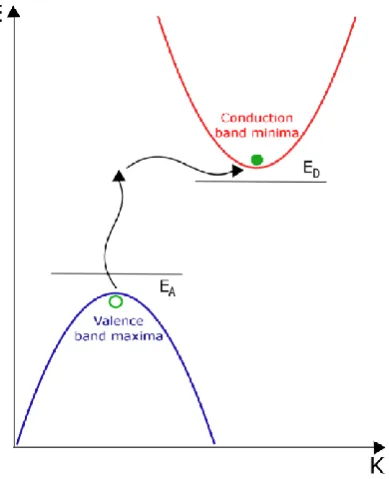
Figure 2.3: Donor and acceptor levels with respect to the conduction and valence bands. The acceptor level is situated just above the valence band maxima, while the donor level is just below the conduction band minima. The blue and red arrows represent the photon and phonon interaction. Along the y axis is energy, and along the x axis is momentum.
Figure 2.4: Representation of diffusion via the vacancy mechanism. Dopant atom is shown as blue.
Figure 2.5: Self interstitial or kick out mechanism. The red atom is the interstitial which may swap with dopant or bulk atom.
Figure 2.6: Adapted from [27], Diffusivities of common dopants in Silicon against temperature.
Figure 2.7: Diffusivities of three main dopants used in Ge against temperature, adapted from [27]
Figure 2.8: Band structure across a pn junction with a reverse bias applied. The applied bias can be seen by the disparity in fermi levels in the p and n regions.
Figure 2.9: Electric field set up in the depletion region of a pn junction.
Figure 2.10: Charge density vs position in a pn junction.
Figure 2.11: pin junction charge density and field with respect to position.
Figure 2.12: A pn junction with reverse biasing, where E ext represents the applied field.
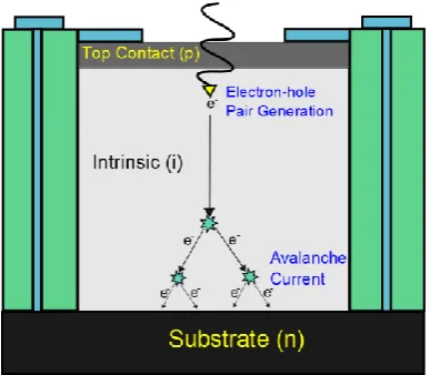
Figure 2.13: Schematic of the avalanche process in an APD. Incident photon is absorbed in the intrinsic region where it is subject to a high electric field, leading to breakdown through impact ionization.
Figure 2.14: Plot demonstrating detection efficiency of several different SPAD devices of varying material design. [43]
Figure 2.15: Example of pulsing the Bias above breakdown for short periods. Precise over bias and dead times depend on the device and its application.
xvii
Figure 2.17: Schematic of a SiGe separate absorption and multiplication SPAD.
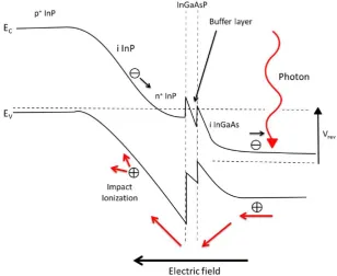
Figure 2.18: Band diagram for III-V SAM-SPAD with buffer layer used to overcome band gap discontinuity issue. Photon is absorbed in the InGaAs before traversing the buffer and undergoing impact ionization in the InP layer.
Figure 2.19:Diagrammatic representation of the photolithography process. Image (a) shows the general photolithography set up. Image (b) shows negative resist, and (c) shows positive resist.
Figure 2.20: Diagram of etching at planes. The substrate (red) is etched away by the TMAH solution leaving the etch resistant epilayer (grey).
Figure 3.1: Schematic of TEM column. Electrons are generated at the top of the column before descending through the various lenses and the sample before
producing an image on the phosphorus screen at the bottom.
Figure 3.2: The three main stages of TEM prep. The grey and silver pieces are the glued gash wafer and the sample respectively. The copper ring is used to mount the sample into the TEM. Unnecessary wafer is removed prior to the milling process. A small hole is formed in the centre of the two pieces of wafer to obtain an electron transparent region.
Figure 3.3: Diagram of basic set up for AFM. The cantilever and tip are rastered across the surface. The incident laser is reflected onto a photodiode, and the
feedback system alters the position using the piezo stage, which is recorded as a change in height.
Figure 3.4: Typical x-ray kit set up. The sample is fixed to the stage, and the source and detector are moveable. The angles represented are 𝜔 (sample to source angle) and 2θ (sample to detector angle). A four bounce Ge crystal was used to produce a monochromatic source.
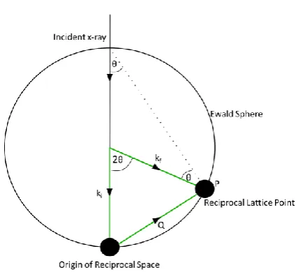
Figure 3.5: The Ewald sphere of reflection demonstrating the diffraction process. The radius of the sphere is 2𝜋/𝜆.
Figure 3.6: Schematic of reciprocal space, with potential visible Bragg peaks. Vertical axis represents [001] direction, and horizontal represents [108] direction. Adapted from [79].
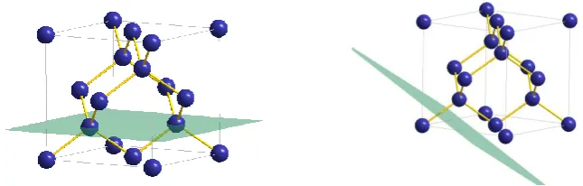
Figure 3.7: Diamond structure showing the (004) and (224) planes.
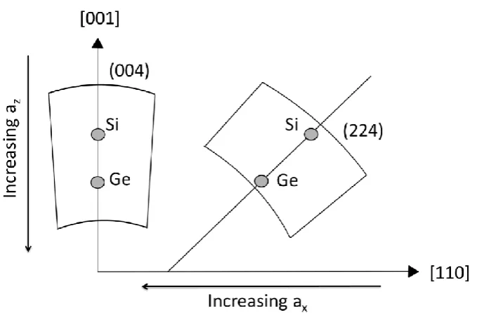
Figure 3.8: Diagram showing RSMs of (004) and (224) for Si and Ge. ax and az are the in and out of plane lattice parameters respectively. Adapted from [79].
Figure 3.9: Schematic of compound refractive lens set up. Circles represent holes in the block. X-rays are focused to a point by the concave lenses.
Figure 3.10: Schematic of 100𝜇m x 100𝜇m areas mapped out across set of suspended wires. The wires (grey bridges) were fabricated with varying thicknesses.
Figure 3.11: Schematic showing the X, Y, Z stage with piezo stage and sample. The suspended sample is positioned on top on the piezo stage and can be moved precisely.
xviii
Figure 3.12: Diagrammatic representation of precursor gas reacting with the surface to form epilayers. The gas molecules are incident on the surface before they are absorbed and any reactions products are removed from the chamber. The dashed bonds represent adatoms which have not yet been absorbed into the lattice.
Figure 3.13: Six major steps for deposition using RP-CVD.
Figure 3.14: The three different growth modes, Frank Van der Merwe (a), Volmer Weber (b), and Stranski Krastanov (c) respectively.
Figure 3.15: Schematic of an RP-CVD system. The lamps are used to heat the chamber and substrate. Precursors are passed through the chamber where the
reactions for growth take place, before the waste gas is removed through an exhaust system.
Figure 3.16: SIMS, the surface is sputtered by a primary ion beam, resulting in ejection of secondary ions.
Figure 4.1: Cross-sectional (220) TEM image in dark field conditions demonstrating the dark areas where growth is becoming non crystalline.
Figure 4.2: Cross-sectional TEM image of Silicon/Silicon-Germanium multilayers grown at a temperature of 700oC. The thin dark lines are SiGe spacer layers. Growth of the Silicon was optimized at temperatures ranging from 500oC up to 800oC.
Figure 4.3: FTIR line scan across the wafer showing the thickness variation of an epitaxially grown Silicon layer.
Figure 4.4: Dark field (220) TEM image of epitaxially grown Germanium with low and high temperature regions.The LT region is the highly defective layer at the interface level, whereas the HT layer is the subsequent region.
Figure 4.5: 3D AFM scan from the surface of Germanium on Silicon with HT and LT growth process. RMS 0.6nm. A cross hatch pattern may be observed on the surface corresponding to the misfit dislocation network at the substrate.
Figure 4.6: Straight through condition TEM image of Germanium and Silicon- Germanium multilayers grown at 350oC. Thin strips are the Silicon- Germanium spacer layers.
Figure 4.7: Diffusion coefficient for Silicon and Germanium interdiffusion against temperature. Adapted from [27].
Figure 4.8: SIMS profile of a Germanium layer grown onto a Silicon epilayer with two step growth. Germanium layer is shown in red, while the Silicon is
represented by the black profile. There is some intermixing at the interface.
Figure 4.9: SIMS profile of arsenic concentration from substrate through into Silicon epilayer. Arsenic concentration segregating into the epilayer can be seen with the decreasing tail in the SIMS profile.
xix
Figure 4.11: SIMS profile comparison of arsenic doped and phosphorus doped Silicon. The detection limit is around 1014cm-3 for this measurement.
Figure 4.12: SIMS profiles of each phosphorus doped silicon sample. Diffusion tails can be observed protruding into each intrinsic silicon region. The doped layers are the rectangular regions in each profile.
Figure 4.13: Table of segregation tail results.
Figure 4.14: SIMS profiles for each phosphorus sample using lower temperature growth, along with LT/HT repeats. A comparison to the As doped layer is also shown.
Figure 4.15: SIMS profile of Ge:B sample 14-292. Layers were grown as alternating doped and undoped layers, with each doped layer having an increased concentration.
Figure 4.16: SIMS profile of Sample 14-291.The layer consists of alternating doped and undoped layers of Silicon and boron doped Silicon respectively.
Figure 4.17: Growth plan for SPAD structure based purely on Silicon. A pin structure is used for absorption and multiplication of incoming photons. Sample ID is Si SPAD.
Figure 4.18: Dark Field 220 diffractive TEM image of top doped layer of Silicon SPAD design (Si SPAD). Highly doped top contact layer can be observed due to the growth stop (dark line).
Figure 4.19: Straight through TEM image of full Silicon SPAD structure (Si SPAD).
Figure 4.20: SIMS plot of the Silicon SPAD measured into the substrate (Si SPAD). Doping concentrations can be observed for the doped and intrinsic regions.
Figure 4.21: Growth plan for SPAD based purely on Germanium. The bottom intrinsic layer grown initially is used as a buffer to minimise TDD in the active region of the device (pin area). Sample ID is Ge SPAD.
Figure 4.22: Cross-sectional TEM image of all Germanium SPAD structure taken under dark field (004) conditions. Ge SPAD.
Figure 4.23: Rocking Curve of the all Germanium SPAD. The doped germanium layer can be seen on the side of the germanium peak. Ge SPAD.
Figure 4.24: Growth plan of separate absorption and multiplication region based on Silicon and Germanium. Sample ID SiGe SPAD1.
Figure 4.25: SIMS profile of SiGe SPAD1. Doped regions and interdiffusion of the Silicon and Germanium are shown.
Figure 4.26: (004) rocking curve of SiGe SPAD1. Asymmetry in the Germanium peak is likely to be caused by some intermixing of the two bulk materials at the interface.
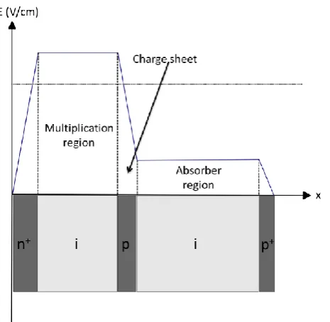
Figure 4.27: Plot showing experimentally determined electric field profile across the absorption and multiplication regions of a SPAD. Adapted from ATLAS data [88].
xx
Figure 4.29: AFM image of doped Germanium surface of SPAD sample 13-312, with RMS roughness 0.6nm. Sample SiGe SPAD2.
Figure 4.30: TEM image of sample 13-312, taken in (004) dark field diffraction condition. Each separate region can be observed according to the growth plan. Sample SiGe SPAD2.
Figure 4.31: HF etched doped Germanium surface of SPAD to demonstrate TDD (6x107cm-2) in sample 13-312. Sample SiGe SPAD2.
Figure 4.32: (004) rocking curve of sample 13-312, with fitted curve (red). The black line represents the measured data. Sample SiGe SPAD2.
Figure 4.33: SIMS profile for SPAD sample 13-312, including top contact and charge sheet. Sample SiGe SPAD2.
Figure 4.34: 2D AFM scan of Germanium doped surface of SPAD structure. The scale on the right describes vertical height, and the top and left axis describe the horizontal position. RMS roughness 0.59nm. Sample SiGe SPAD2.
Figure 4.35: Dark field (004) images of other SPAD structures grown to the same design as 13-312. The top image shows the full structure down to the substrate, whereas the bottom image confirms the existence of the highly doped
Germanium boron top contact. The white dashed lines represent the doped layers. Sample SiGe SPAD2.
Figure 4.36: SIMS profile of arsenic concentration in Silicon from the substrate. The highly doped region represents the doped substrate that the structure was grown on. Sample SiGe SPAD2.
Figure 4.37: SPAD growth structure with epilayer n-type bottom contact. Sample SiGe SPADn.
Figure 4.38: Examples of 2D AFM scans for SPAD structure with n-type (GeB) epilayer. Height range is shown on the right axis, while the left and upper axis describe the lateral position. RMS roughness 0.65nm. Sample SiGe SPADn.
Figure 4.39: Dark field (004) TEM image of Germanium absorber region in SPAD. Sample SiGe SPADn.
Figure 4.40 a and b: Dark field (004) TEM image of full structure of SPAD (a) and top p-type (GeB) top contact (b). Sample SiGeSPADn.
Figure 4.41: Optical image of SPAD device. Top contact pad is shown on the right, bottom contact pad on the left. The largest device is 500µm.
Figure 4.42: SPAD device with fabrication steps, Nickel contacts, and Silicon Nitride passivated side walls.
Figure 4.43: TEM image of sample used for fabricated SPAD devices, ID 13-191, taken in straight through condition.
xxi
Figure 4.45: Plot of dark currents for different mesa sized SPAD devices (13-191)
measured at low temperature (77K). Reverse bias is applied, using a probe station, to each SPAD device and is increased up to 40V (instrumental limit). Breakdown of each device is observed by the sudden increase in current up to the saturation limit (0.04A).
Figure 4.46: Plot of dark current for SPAD device (14-329) measured at room
temperature. Reverse bias is applied, using a probe station, to each SPAD device and is increased up to 40V (instrumental limit). 1, 2, and 3 represent the 1st, 2nd, and 3rd repeat of the measurement.
Figure 4.47: Plot of dark current for SPAD device (14-329) measured at room temperature. 4 different “light levels” were used to test the devices photoresponsivity. Reverse bias is applied, using a variable temperature probe station, to each SPAD device and is increased up to 40V (instrumental limit).
Figure 4.48: Comparison of room temperature dark current measurements with increasing applied reverse bias for samples 14-329, and 13-191.
Figure 4.49: Plot of dark current for SPAD device (14-329) measured at low temperature (77K). Reverse bias is applied, using a probe station, to each SPAD device and is increased up to 40V (instrumental limit). Breakdown is observed at the point of sudden increase in current.
Figure 4.50: Plot of dark current for SPAD device (14-329) measured at low temperature (77K). 4 different “light levels” were used to test the devices
photoresponsivity. Reverse bias is applied, using a variable temperature probe station, to each SPAD device and is increased up to 40V (instrumental limit).
Figure 4.51: Plot comparing dark current for SPAD device (14-329) measured at low temperature (77K) and room temperature. Reverse bias is applied, using a probe station, to each SPAD device and is increased up to 40V (instrumental limit). Breakdown is observed at the point of sudden increase in current.
Figure 4.52: Initial results demonstrating photon detection at 1550 nm and under dark conditions for new structure SPAD device (14-329) (100𝜇m diameter active area).
Figure 4.53: Single photon detection efficiency (SPDE) at 1310nm, and DCR for SPAD sample (25𝜇m diameter), as a function of excess bias for sample 13-312.
Figure 4.54: Summary graph of a selection of SPAD devices using different materials at different wavelengths. Data points are taken from Table 4, with SPDE results from this work also included (circled).
Figure 5.1: Growth plan for SiB epilayer. Doped Silicon layer is grown onto nominally undoped substrate.
Figure 5.2: Dark field (220) TEM image of sample 12-019.
Figure 5.3: Dark field (004) TEM image of sample 12-020.
Figure 5.4: Dark field (220) TEM image of sample 12-270. On set of
xxii
Figure 5.5: Dark field (220) TEM image of sample 12-135. Due to a thinner critical thickness dislocations can be seen to be forming in the layer.
Figure 5.6: Dark field (220) TEM image of sample 12-016. Polycrystalline mounds can be seen around the dark areas in the epilayer.
Figure 5.7: 3D AFM scan of the surface of samples 12-020 (a) and 12-023 (b).
Figure 5.8: Bright field (220) TEM image of sample 12-023. Small dark dots in the epilayer are thought to be clusters of atoms or areas of polycrystallinity.
Figure 5.9: (004) Rocking curve for sample 12-020 with fitting curve (red). SiB peak can be observed to the right of the Silicon peak accompanied by thickness fringes.
Figure 5.10: (004) rocking curves for samples 12-268 and 12-270. Sample 12-268 was a sample with essentially intrinsic doping for comparison.
Figure 5.11: Plot of sheet resistance for each SiB sample. Measurements are taken at regular intervals of temperature .All samples are highly boron doped, except for sample 12-268, which was essentially intrinsic, therefore showing
semiconductor resistance nature. Sample 12-268 is not shown on this plot due to its much higher resistance compared to all other samples.
Figure 5.12: Carrier concentration for each SiB sample, measured by VdP. Data is excluding sample 12-268, which had a carrier concentration much lower than other samples.
Figure 5.13: Plot describing 𝛽 values obtained for Equation 5.1. Red data represents hall data, and black shows XRD. Gradient of each fit gives β value.
Figure 5.14: Plot demonstrating the results from this work compared to solubility limits at different growth temperatures. The red data point shows an order of
magnitude increase to the doping concentration above the solubility limit at 700oC.
Figure 6.1: Thickness calculations from (004) rocking curves for each sample against etch time. When the sample is etched away (or becomes too thin) no thickness fringes are observed. Therefore the sample is considered not etch resistant (shown by the dashed line).
Figure 6.2: Optical image of defined membrane square after photolithography process and pre etching Membrane fabricated were 1mm x 1mm in size.
Figure 6.3: SEM image of a set of fabricated SiB wires, according to the process described in section 6.1.1.2, used for synchrotron measurements.
Figure 6.4: Out-of-plane lattice parameter plot from across the membrane, using (004) reflection calculations. The red area represents the corner of the suspended membrane, and the green region is the bulk SiB material. The lattice
parameter is at its largest at the membrane edge before decreasing slightly towards the middle.
Figure 6.5 Schematic of set of SiB wires showing the level of tilt across them. Areas of increased tilt are shown in red and green.
xxiii
Figure 6.7: RSM taken from the wires where the tilt appears to be the same as the bulk area.
Figure 6.8: RSM taken from the wires where the tilt appears to be different to the bulk area.
Figure 6.9: SEM image demonstrating an example of some dirt, highlighted by the arrows, on the wires. The dirt is seen by the small lightly coloured regions, which are thought to disrupt the x-ray signal and lead to a potentially
phantom tilt.
Figure 6.10: Out-of-plane lattice parameter plot from across the wires, using (004) reflection. The general trend is an increase in out-of-plane lattice parameter on the wires which is thought to be caused by their uniaxial nature. Some of the wires do not line up due to the meshing of the data during analysis.
Figure 6.11: SEM image of a set of SiB wires highlighting the suspended shelf adjacent to the wires.
Figure 6.12: (004) map describing the shift in qx for the corner scan of the membrane. The most amount of tilt is present at the corner of the membrane.
Figure 6.13: Line scan showing lattice parameter variation from edge to centre of membrane. Approximate error bars have been added to show the small deviation across the measurements.
Figure 6.14: Line scans from both wires and membrane. The top and right axis are for the membrane, and the bottom and left axis are the wires. The overall trend for lattice parameter is to increase on the wires and decrease across the
membrane.
1
Chapter 1
Introduction to Silicon and Germanium
1.1 The Semiconductor industry 2
1.2 Photon-detection 3
2
1.1 The Semiconductor industry
Since the creation of the first transistor at Bell labs in 1947 Silicon has been the
dominant semiconductor material used in the industry, accounting for 97% [1]. The
semiconductor industry has been estimated to reach over $350 billion in total sales
by 2016 [2]. Silicon became the preferred option due to its low cost for integrated
circuits. Despite some material properties being inferior compared to other
semiconductor materials such as Germanium, the availability and cost advantages
of Si significantly outweigh these. Added to this, a high thermal conductivity of
Silicon also reduces overheating in the circuits.
Probably the most common application for Silicon as a device is in the
metal-oxide-semiconductor-field-effect-transistor (MOSFET). The oxide of Silicon
(SiO2) has excellent insulating qualities making it ideal for device fabrication [3].
The scale of these devices is constantly being reduced so that the density of
transistors on an integrated circuit can be increased, resulting in smaller systems.
The number of transistors used follows Moore’s law, stating that the number of
transistors on an integrated circuit doubles roughly every two years.
As previously mentioned, if price was disregarded, Silicon would not be the logical
choice to base semiconductors around. For some applications, examples which are
not limited to Germanium or an alloy of Silicon and Germanium may be more
suitable. However in the case of Germanium, the cost and fragility of Ge substrates
prevents them from being a viable option for mass production. Instead Germanium
can be grown epitaxially onto the much cheaper Silicon substrate. Unfortunately
the cost of growing other materials is not necessarily a cheap process, and may
require long growth times. Also the heteroepitaxy (growth of a layer which is
different from that preceding it) introduces negative side effects which can result in
poor quality layers. As epitaxial growth has been improved techniques have been
employed to obtain relatively smooth and defect free layers of materials such as
Germanium. With better quality layers, new devices and enhancement of existing
ones can be realised. Germanium is used in laser devices [4], solar cells (with III-V
materials) [5], and infra-red (IR) photodetectors [6]. It is also grown as an alloy for
various applications. Silicon is the most common choice, where Silicon
3
substrate [7]. Tin has also become a promising material to use in an alloy with
Germanium, as it has been predicted that a direct band gap can be obtained at 12%
tin content [8].
1.2 Photon-detection
The detection of single photons has many applications in areas such as
biophotonics where the number of photons emitted is often very small [10]. The
semiconductor band gap plays an important role in the performance of many
devices: one of which is the ability of a semiconductor to absorb photons. For
applications in the telecommunication region, wavelengths above 1 𝜇m and up to
1.55 𝜇m are of particular interest. The semiconductor material chosen for an
application will be dependent on its band gap, and therefore the wavelengths
accessible. Table 1 shows a table of semiconductor and III-V materials and their
respective band gap.
Table 1: Band gap values for relevant semiconductor materials. Taken from
[10][11].
Material Band Gap
(eV)
Lattice Parameter
(A)
Absorption Limit
(nm)
Silicon 1.11 5.43 1550
Germanium 0.66 5.66 1000
Indium
Phosphide 1.27 5.87 960
InGaAs
(variable) 0.73 5.65-6.05 1680
If the energy of a photon is sufficiently large, such that its energy is equal to or
exceeds the value of the band gap, it may be absorbed. Shorter wavelengths have a
larger energy according to:
𝐸 =
ℎ𝑐4
From equation 1.1 it can be seen that for a given band gap there will be a maximum
wavelength of photon that can be absorbed. Therefore clearly some materials are
unsuitable beyond a specific wavelength so cannot be used in a device which is
dependent on detection of such a wavelength. For an alloy of Silicon and
Germanium, a mere 5% Silicon can lead to a bandgap of nearly 0.2 eV greater than
that of Germanium [12]. This can be problematic for any structures which require
small band gaps for detection of near infra-red photons.
The absorption of a photon is not the only important factor in photodetection. Once
a photon is absorbed it has to be detected. The absorption of a photon may create
an electron-hole pair which can then be detected via an external source. The first
device to demonstrate this was the photomultiplier tube (PMT), which was
designed in 1930 by Russian physicist Kubetsky. The experiment used primary
photoelectrons emitted from a photocathode and accelerated them into consecutive
emitters. At each emitter further secondary electrons could be emitted and undergo
the same process resulting in a huge amplification. Gains of up to ten thousand
were recorded [13].
The process of photodetection has evolved since this invention with the help of
semiconductors. Using the same concept as the PMT, avalanche photodiodes have
been established as a compact and integratable device. However, this market has
been dominated by III-V materials due to their more appropriate band gap when
operating at the principal telecommunication wavelengths of 1330 nm and 1550
nm. Despite this apparent monopoly in these devices, other materials are used and
do have some advantages over their III-V competitors. Silicon and Germanium are
the main rivals to III-V photodetectors and are explored further in this piece of
work [1].
1.3 Summary
Photon detection has long been an important part of the communications industry,
with interest in a wide range of wavelengths. Avalanche photodiodes are one
method of detection, with a more recent focus on detection of weak signals in the
infrared region of the spectrum, the limit of which requires detecting single
photons. Silicon and Germanium are two materials which may be used to form
5
designs have generally been considered to be the most promising for industrial
devices.
This work explores the potential of Silicon and Germanium Single photon
avalanche diodes (SPADs), particularly for application to the low energies of
infrared photons. It has led to the production of the first successful detection of
single photons with a wavelength of 1.55 𝜇m, as well as impressive results at 1.33
𝜇m that compare favourably to those obtained using similar III-V devices. Material
characterization and electrical measurements from this work may be used to further
advance the designs of future devices.
Work and development into the doping of semiconductors, specifically Silicon and
Germanium, via chemical vapour deposition has also been accomplished. Much of
the work can be useful in a wide range of growth applications for improving device
performance, as well as for initial work into the suspension of doped Silicon boron
layers. High doping essentially transforms a semiconductor into a material with
metallic properties, which is important for low contact resistance pads for many
different devices.
In relation to SPAD devices, there is an interesting possibility for the incorporation
of suspended structures which will also be explored in this thesis. While this has
the benefit of removing the dislocation networks for mismatched materials, there is
also the possibility of reducing the leakage current, as well as introducing a
6
Chapter 2
Background Theory
2.1 Basic Properties of Si and Ge 7
2.2 Strain enhancement 8
2.3 Doping semiconductors 11
2.3.1 Dopant Migration via diffusion and segregation 16 2.3.2 High Doping Concentrations 17
2.4 pn junctions 18
2.4.1 Biasing pn junctions 20
2.5 Single Photon Avalanche Diodes 21
2.5.1 Dark Counts 26
2.5.2 Afterpulsing and Device operation 28 2.5.3 Single Photon Avalanche Diodes designs (Si and Ge or III-V) 29
2.6 Photolithography Processes 35
2.7 Suspended Membranes and Wire 37
2.7.1 Etching 37
2.7.2 Membrane etching 38
7
2.1 Basic Properties of Si and Ge
Probably the most important and exploited properties of a semiconductor are its
band gap and the mobility of its charge carriers. The band gap is characterized by
the energy required to form an electron hole pair in the conduction and valence
band respectively. Figure 2.1 shows a 1D representation of the band gap.
Figure 2.1: Electron excitation leaving a hole in the valence band. The gap
between the two bands is the band gap. Energy levels below are core levels.
A semiconductor’s band gap may be either direct or indirect. A direct band gap is
observed when the maximum of the valence band and the minimum of the
conduction band both lie at k = 0. This is the preferred method of excitation as a
photon of appropriate energy can excite an electron directly from the valance band
to the conduction band. An indirect band gap is seen when the conduction band
minima are not aligned with the valance band maximum at k = 0. This instead
means that, for a transition to take place, a change of electron momentum is
required as well as absorbing the energy of a photon. This momentum can be
supplied through a phonon. The two materials used throughout this work are
Silicon and Germanium which have band gaps equal to 1.12 eV and 0.67 eV
respectively [14], both of which are indirect.
Mobility is of great importance in devices such as transistors, describing how easily
carriers are able to traverse through the material. A low mobility of carriers results
in slow transistor performance. Both carrier types, electrons and holes, have a
unique value for mobility in a given semiconductor material (at a particular
temperature). The mobility is given by 𝜇 = 𝑣
𝐸 where the mobility is 𝜇, the drift
8
higher drift velocity, and therefore faster transistors, a material with high mobility
is preferable. Bulk Germanium has higher electron and hole mobilities when
compared to bulk Silicon, which is partly why it has attracted such interest in
semiconductor research. However as previously described, the limiting factor
which prevents this superior material from surpassing Silicon is its much higher
cost.
A crystal lattice is observed where atoms are bonded at regular periodic sites. Both
group IV semiconductors, Silicon and Germanium, have a diamond-like lattice
structure. This is represented by two face centred cubic lattices which are displaced
by a quarter of the diagonal of a cubic unit cell along its diagonal. Each atom in the
lattice is bonded to its four nearest neighbours covalently. This results in a
tetrahedral system where the atoms are separated by a length described as the
lattice constant. Germanium has a larger lattice constant (5.658 Å) than Silicon
(5.431 Å) which is important when growing these materials together. For pure
Germanium on Silicon there is a 4.2% lattice mismatch which affects the quality of
the Germanium layer. It should also be noted that an alloy containing both Silicon
and Germanium can be grown (Si1-xGex), which will have its own unique lattice
constant, defined by the amount of each material (x) in the structure [15].
These alloy structures can also be useful for band gap engineering. Levels of
Silicon or Germanium can be altered to tune to a required band gap. This can be
useful for photonic applications in which for example, the band gap of Silicon is
unsuitable. Interestingly the band gap of SiGe has two different phases depending
on the Germanium content. The band gap is Silicon-like up to 85% Germanium,
before it becomes Germanium-like. The equations which relate the Germanium
content (x) and the band gap are [16]:
𝐸
𝑔= (1.155 − 0.43𝑥 + 0.0206𝑥
2)𝑒𝑉
for x < 0.85𝐸
𝑔= (2.010 − 1.27𝑥)𝑒𝑉
for x > 0.852.2 Strain enhancement
The mismatch experienced between differing lattice parameters can be exploited
when improving device performance. As previously stated Silicon and Germanium
9
pseudomorphically onto a Silicon (Germanium) substrate the lattice parameter of
the epilayer matches that of the substrate. This induces strain into the epilayer as
the lattice parameter is either compressed or stretched so that the atomic positions
align with those in the underlying layer.
When there is this significant build-up of strain between two layers, the most
common relief of this is through dislocations. A dislocation is the boundary of a
slipped plane. Dislocations [17-19]occur in both the (110) and (111) planes which
is useful in diffractive imaging in a transmission electron microscope as stacking
faults do not appear in orthogonal diffractive conditions. A misfit dislocation is
formed at the interface and is found along the (110) plane, shown in Figure 2.2.
Threading arms protrude from the misfit dislocations along the (111) plane and
terminate at another surface. The displacement direction, and its magnitude, of the
lattice which leads to the formation of threading dislocations is characterized by its
burgers vector. Movement of the dislocations occurs along the (111) plane, and is a
common method of lowering their density.
Figure 2.2: Diagrammatic representation of a misfit and threading
dislocation. The threading arms direction is defined by the 60o burgers vector
shown in the (011) direction.
As the strain builds up in a layer, the energy increases. At a given value the energy
becomes high enough so that a row of covalent bonds may be broken, resulting in
the aforementioned slipped plane. At this point the energy exceeds the activation
energy required for nucleation of dislocations and relaxation will take place. The
point at which a layer undergoes this procedure is known as the critical thickness.
10
dislocations. The critical thickness is dependent on both the bulk layer and the
lattice matched layer. Large mismatches between layers reduce the critical
thickness, and may result in only a few monolayers of growth before the onset of
dislocations. The relatively large mismatch between Silicon and Germanium
prevents the growth of thick layers (of the order of tens of nm [20]), free of
dislocations.
In the case where Germanium is grown directly onto Silicon far beyond the critical
thickness there will be a large density of dislocations, particularly around the
interface. A characteristic measure of this is termed the threading dislocation
density (TDD), and refers to the number of threading dislocations observed in a
given area. There are methods of counting, usually directly by plan view TEM or
by selective etching to create pits at the dislocation sites, and reducing the number
which can be employed to reduce this number. One of which, annealing [21],
utilises the potential for the threading dislocations to move and annihilate, therefore
reducing the TDD. When subject to suitably high temperatures dislocations are
able to glide. Physically the bonds may be reattached at the boundary while others
are broken creating an apparent glide of the dislocations. Under these
circumstances dislocations may glide all the way to the edge of the structure or
they can annihilate when the meet another dislocation. Unfortunately simply
annealing a sample to lower the TDD via this method has the drawback of
migration of bulk atoms and dopants from their desired location.
Throughout this work the strain in a layer was calculated using:
𝜀
𝑝𝑒𝑟𝑝=
𝑎𝑝𝑒𝑟𝑝−𝑎𝑆𝑖𝐵𝑎𝑆𝑖 Equation 2.1
Where the denominator defines what the strain is with respect to. In this case it is
the Silicon substrate, but could also be with respect to the bulk material. The
perpendicular strain describes that of strain parallel to the growth direction. This
equation is specific for a SiB on Silicon system. A negative perpendicular strain
value corresponds to a biaxial tensile strain, whereas positive is a compressive
strain. For an elastic system this will correspond to an opposite strain value in the
11
As the biaxial strain in a layer is increased there is a splitting of the bands. For the
valence band there is a splitting of the heavy hole band (HH) and the light hole
band (LH) (breaking the degeneracy). For a compressively strained system the HH
shifts up and the LH shifts down in energy, relative to their common original
energy in the unstrained system. For a tensile strained system the opposite is true.
The splitting of the valance bands reduces the scattering between the bands, while
the alteration of their curvature (in E-k space) changes the hole effective mass.
Meanwhile, the conduction band is shifted to lower energy and, if enough strain is
applied, it is possible to change some materials from an indirect to a direct band
gap semiconductor. A further result of the reduced scattering rate and reduced
effective mass is that the mobility is increased.
2.3 Doping semiconductors
There are two different possible types of dopant for a Group IV semiconductor.
These are namely donors and acceptors. A donor will be a Group V material such
as phosphorus or arsenic, which have five outer shell electrons. When bound to
other Group IV atoms four of these electrons do so covalently. The fifth electron
which is left over can occupy a state in the conduction band. This is characterized
by a state called a donor level which is present just below the conduction band, and
has a much smaller energy required to free it (typically tens of meV compared to
~1 eV for the band gap). An acceptor on the other hand is a Group III atom,
typically boron. When this atom forms four covalent bonds with Group IV atoms
there will be a missing electron. This represents a hole in the valence band and is
characterized by an acceptor level, analogous to the donor level around the
conduction band. These extra energy levels are actually only detached from their
respective band, shown in Figure 2.3, meaning that at T = 0 K the valence band
will still be just full of electrons.
Diffusion in semiconductors is a generally detrimental effect which can lead to
performance issues in devices. Essentially it is the migration of atoms from their
lattice points through point defects, and may affect both foreign and intrinsic
atoms. Dopant diffusion relates to the movement of dopant atoms through the
12
Both of these types of diffusion are undesirable and impossible to irradiate
completely.
Figure 2.3: Donor and acceptor levels with respect to the conduction and
valence bands. The acceptor level is situated just above the valence band
maxima, while the donor level is just below the conduction band minima. The
blue and red arrows represent the photon and phonon interaction. Along the y
axis is energy, and along the x axis is momentum.
There are two main ways in which diffusion is mediated in semiconductors. They
are via namely vacancies and self-diffusion. The vacancy mechanism for diffusion,
shown in Figure 2.4 is seen where an atom jumps to a neighbouring vacancy site
(which is essentially the absence of an atom in the lattice structure). This process
may repeat if a vacancy becomes present in a neighbouring lattice site.
For the self-interstitial mechanism, a self-interstitial, which is present in the lattice,
will exchange position with a lattice atom so that it is free to migrate through the
lattice. This atom will act as a self-interstitial and move through the lattice until it
exchanges with another interstitial. For dopant diffusion this is known as the kick
out method but is the same as for the bulk self-interstitial mechanism, which is
[image:34.595.229.424.121.361.2]13 Figure 2.4: Representation of diffusion via the vacancy mechanism. Dopant
atom is shown as blue.
The basic equations which describe these two methods are (𝐴𝑉) ↔ 𝐴𝑠+ 𝑉 and
𝐴𝑖 ↔ 𝐴𝑠 + 𝐼 for vacancy and self-interstitial methods respectively. Here Ai is the
interstitial dopant and As is the substitutional dopant. The diffusion of atoms is
associated with the heat or thermal energy it is given and the diffusion coefficient,
which is given by
𝐷 = 𝐾exp (−
𝐺𝑘𝑇
)
Equation 2.2
Where G is the Gibbs free energy, and K is a constant. When G is substituted for
∆𝐺 = ∆𝐻 − 𝑇∆𝑆
Equation 2.3The diffusion coefficient can be expressed as
𝐷 = 𝐷
0exp (−
𝐻𝑘𝑇
) = 𝐷
0exp (−
𝐸𝐴
𝑘𝑇
)
Equation 2.4 Where 𝐷0 incorporates the 𝑇∆𝑆 term, and 𝐸𝐴 is the activation energy of the dopantatom. Clearly, an increase in temperature in the system gives rise to a larger
diffusion coefficient. With a higher diffusion coefficient an atom will diffuse
further from its original lattice site. This can be a major problem for precise and
abrupt doping profile and interfaces. Typical distances travelled during growth,
estimated through Figure 2.6, are of the order of tens of nm, over growth time of
14
concentrations should be close to background over 10-100 nm, it is important to
select appropriate growth conditions to maximise the chance of this.
Figure 2.5: Self interstitial or kick out mechanism. The red atom is the
interstitial which may swap with dopant or bulk atom.
In Silicon, dopants diffuse through a mixture of self-interstitial and vacancy
mechanisms. Boron diffuses through Silicon via the self-interstitial mechanism.
This is much faster than n-type diffusion and self-diffusion of Silicon demonstrated
in Figure 2.6. There is little data for diffusion in Silicon at temperatures below
around 800oC. Therefore the diffusion data of dopants in Silicon presented here is
for temperatures higher than those used for this work. However, the general trend
can be seen and the level of diffusion in Silicon at room temperature is quite low.
At relatively high temperatures used for a long period of time the diffusion may
become quite significant.
The diffusion of dopants in Germanium is dependent on which type of doping is
present. For n-type dopants the vacancy method is the mechanism by which the
atoms diffuse [28]. There is an attractive coulomb interaction between the
vacancies and n-type dopants such as P, As, and Sb, which is why this diffusion is
faster than self-diffusion of Germanium. Boron is the most researched [29, 30
]p-type dopant in Germanium, and is seen to be much slower at diffusing when
compared to n-type dopants and even self-diffusion of Germanium, which is shown
in Figure 2.7. As there is a low concentration of self-interstitials in Germanium it is
15
0.6 0.7 0.8 0.9 1.0
10-20
10-19
10-18
10-17
10-16
10-15
10-14
Diffusivity (
m
2 s -1 )
1/T (10-3 K-1) B P As
1300 1200 1100 1000 900 800 T (o
C)
Figure 2.6: Adapted from [27], Diffusivities of common dopants in Silicon
against temperature.
There are advantages and disadvantages to each different method of introducing
dopants into the material. Implantation is likely to damage the layer of bulk
material inducing large numbers of defects. A common way to counter this is to
anneal the layer subsequently, which will cause diffusion of the dopants away from
the desired area. Diffusing dopants into a layer is difficult to control and is a
difficult process when not doping the surface layer. Doping via the epitaxy method
does take accurate control of many different growth parameters, which is often
challenging, but when performed successfully produces abrupt and accurately
doped layers. In particular, when this is done via CVD the structures can easily be
reproducibly grown and on a large scale.
In an ideal situation all the dopant atoms may be incorporated into lattice sites and
therefore all contribute to the electrical properties of the semiconductor. However
in reality each dopant species has a solubility limit, which can prevent efficient
doping in an epitaxial layer. These solubility limits in Germanium and Silicon
range from 1018cm-3 to 1020cm-3[31]. Doping up to this limit allows all the dopant
atoms to occupy lattice sites, and therefore be electrically active. Above these
limits dopants start to fill non-lattice sites known as interstitial sites. When
16
conductivity of a device. Furthermore, when too many atoms are in interstitial sites,
and therefore not in the diamond lattice sites, the crystal structure may be
disrupted. Clustering of these atoms can result in areas where a different crystal
structure begins to form and cause a polycrystalline layer to grow.
0.9 1.0 1.1 1.2 1.3 1.4 10-20
10-19 10-18 10-17 10-16 10-15 10-14
Diffusivity (
m
2 s -1 )
1/T (10-3 K-1) B
P
As
900 800 700 600 500
T (oC)
Figure 2.7: Diffusivities of three main dopants used in Ge against
temperature, adapted from [27]
2.3.1 Dopant Migration via diffusion and segregation
Ideally a doped layer will retain its profile throughout other treatment post growth.
However migration of dopants is often problematic when subjecting structures to
elevated temperatures. Procedures commonly use high temperature growth when
not doping a layer, or undergo annealing steps to aid the reduction of TDD for
example. This increase in temperature leads to diffusion of atoms, whether they are
bulk atoms or dopant atoms. Unfortunately this is unavoidable in epitaxial systems
as well as other techniques such as implantation. The natural side effect is that
either intermixing of layers takes place, for example forming a SiGe layer around a
Silicon and Germanium interface, or the doping profile in a structure becomes
smeared. Many devices rely on an abrupt and uniform doping profile for operation,
which if effected will prevent optimal device operation. For example in an
avalanche photodiode abrupt doping profiles are required for a precise electric field
17
which could prevent transport of the carriers, give insufficient energy gain for
carrier avalanche, or potentially eliminate the field entirely.
2.3.2 High Doping Concentrations
One area of interest for semiconductor application is to dope at such high
concentrations that the doped layers begin to exhibit metallic behaviour. This can
be used for device contacts, in transistors, and even as an etch blocker.
Unfortunately when trying to incorporate high levels of dopants into a bulk crystal
such as Germanium or Silicon the quality of the grown layers may be sacrificed.
This is mainly due to the issue of passing the solid solubility limit as mentioned in
the previous section. In this work I will focus on obtaining high levels of the p-type
dopant boron in the Silicon lattice.
Relatively little work has been directed towards highly doped SiB layers,
particularly by RP-CVD. Some of the highest Boron concentrations reported are by
GS-MBE, up to approximately 1021cm-3[31]. Other reports have been presented
with an electrically active dopant level of around 1020cm-3 for both SS-MBE and
UHV-CVD [32, 33]. The main drawback for producing highly doped SiB samples
via MBE time on a mass scale is the increased growth. Although thin layers may be
relatively fast to grow in both systems, when including them in other larger and
thicker structures the CVD holds a clear advantage from an industry point of view.
The solubility limit of boron in Silicon is dependent on the temperature of epitaxial
growth. Several reports have shown that the solubility of boron in Silicon is around
8x1020cm-3 at 1400oC, 1x1020cm-3 at 1000oC, and 2x1019cm-3 at 700oC [34-36]. In
this work, most of the growth of doped layers has been at around 700oC. Higher
temperatures such as 1400oC are outside the range of RP-CVD and are likely to
experience more significant diffusion than at 700oC which can be a significant
problem for devices that require abrupt profiles.
It is possible to incorporate dopant atoms into a layer at lower temperature
(300/400oC) by using non-equilibrium techniques, similar to that used for
Germanium tin growth [8]. These techniques involve absorbing molecules onto the
surface which already have the dopant atom “locked in”, and for this molecule to
remain stationary. This technique is often slow and complicated, which is seen in
18
substantially increase the cost. This work however focuses on growth at higher
temperatures (700ºC) under equilibrium growth conditions.
2.4 pn junctions
As for many nanoscale devices the basis of a SPAD is a pn junction. These
junctions may be used for rapid change of current flow in order to change the state
of the device. Fundamentally, a pn junction is simply a region of p doped material
adjacent to an doped region, but the diode relies on accurately doped p- and
n-regions for precise operation. Doping may be performed via implantation,
diffusion, or epitaxy as described previously. Initially a pn junction will be
described under no bias (no external field), where there will be no current in the
junction. The p-region will have a fermi level situated just above the valence band,
and the n-region will have a fermi level placed just below the conduction band.
Under zero external bias when these materials are joined the fermi level must be
uniform across the structure. When the p- and n-regions are brought into contact,
free electrons in the n-type material may diffuse across the junction and recombine
with a hole on the p-type side. This will create a negative ion and leave a positive
charge in the p-region.
Figure 2.8: Band structure across a pn junction with a reverse bias applied.
The applied bias can be seen by the disparity in fermi levels in the p and n
regions.
A result of forming the pn junction is a built in voltage. This represents the
potential required to move a carrier across the depletion region, and is dependent
on the band gap, acceptor level, and donor level. An applied bias can also alter the