ECE250 Getting Started with Cadence Orcad Lite V. 9.2
Prepared by Keith HooverDept. of Electrical and Computer Engineering Rose-Hulman Institute of Technology
Terre Haute, Indiana 47803
1. Introduction to SPICE and PSPICE
SPICE is an electronic circuit simulation tool that was developed at the University of California at Berkeley in the mid 1970’s. SPICE is an acronym that stands for “Simulation Program with Integrated Circuit Emphasis”. It was developed specifically for use in verifying the proper operation of new integrated circuit designs before they are ever committed to silicon. Therefore, SPICE had to yield very accurate predictions of circuit performance, since many dollars are at stake when committing a new IC design to silicon!
SPICE soon became a very popular industrial and academic general circuit simulation tool, because it was developed under U.S. government funding and was therefore distributed free of charge to any U.S. citizens. Early versions of SPICE were confined to run on large computer mainframes that used the UNIX operating system, but soon SPICE programs capable of analyzing relatively small circuits were migrated to run on the IBM PC platform in the early 1980’s, as the IBM PC came into widespread use The original SPICE program required a “net list” description of the circuit to be entered. (The net list was also called a “simulation SPICE deck” in the old days of computer punched cards.) In the net list, each circuit component must be entered on a line that contained a label that denoted the component type, the component value, and the node numbers across which the device is connected. Making a net list required drawing the schematic and then numbering the nodes. (The ground node must be numbered “0”, but the rest of the node numbering is arbitrary).
PSPICE is an enhanced commercial version of SPICE. PSPICE was first marketed by MicroSim. Then MicroSim was bought by OrCad, which was in turn recently acquired by Cadence. Orcad PSPICE has a very useful “schematic capture” front end “pre-processing” program called “CIS Capture”, that allows the circuit schematic to be drawn on the computer screen, and then PSPICE automatically numbers the nodes and generates the net list. PSPICE also has a very nice graphical plotting “back end” program called “PROBE”. Using the PROBE graphical post-processor, the PSPICE output can be plotted. Multi-trace plots are easily generated. A set of X-Y cursors can be employed to read and display precise values at any desired point on any selected waveform.
Orcad Lite Version 9.2 PSPICE is a “crippled” freeware demonstration version of the commercial industrial-strength version of Cadence’s Orcad SPICE that can run on a wide variety of computer platforms, including the inexpensive IBM-compatible PC’s. By “crippled”, I mean that a number of restrictions have been intentionally built into the freeware version, which seldom hamper the student who desires to simulate and study simple basic electronic circuits containing only a few components, but would make it impossible to simulate most of the more complex practical industrial circuits. This clever so-called “crippleware” scheme has made MicroSim Demo PSPICE, and now Orcad Lite PSPICE, by far the most popular educational circuit simulation tool. The overwhelming academic acceptance of PSPICE “crippled freeware” has contributed to the success of the commercial version of this product, as students trained to use the PSPICE freeware have graduated and entered industry. PSPICE has become the defacto standard academic circuit simulation software, and it is covered in depth in dozens of recent electronics textbooks.
Some of the more notable limitations of the Orcad Lite crippleware Version 9.2 PSPICE are listed below:
Orcad Lite V. 9.2 PSPICE Freeware Limitations
1. Schematic drawings limited to a maximum of 60 instances of the same part. 2. Simulations limited to a maximum of 64 nodes.
3. Simulations limited to a maximum of 10 transistors. (Each OP AMP model contains 2 transistors.) 4. Simulations limited to 10,000 digital logic level transitions.
5. Simulations limited to a maximum of 10 transmission lines.
6. Only a subset of the component PSPICE simulation libraries are made available, though more can be downloaded from the internet using the Capture CIS (component information systems) program.
2. Types of Analog PSPICE Simulations
There are several distinct types of analog PSPICE simulations: DC quiescent operating bias point calculation, transient analysis, sinusoidal steady-state “AC sweep” (frequency response) analysis, and “DC sweep” (voltage transfer curve) analysis.
DC quiescent operating “bias point” calculations are performed automatically, since the DC operating point must be known in any electronic circuit containing diodes or transistors before the AC behavior of the circuit can be determined.
Time-Domain Transient analysis simulations are probably the most popular type of PSPICE analysis, where one or more time-varying response waveform(s) are calculated based upon one or more specified time-varying input source waveform(s). Various types of input source waveforms are available for transient analysis. The most popular transient simulation sources are the sinusoidal voltage source (VSIN), voltage pulse train (VPULSE), exponential voltage source (VEXP), or piecewise-linear voltage source (VPWL), where any piece-wise linear waveform may be ascribed to the source. In addition, VPULSE has the following special cases: square wave (Vsq), triangle wave (Vtri), saw-tooth voltage source (Vramp), and TTL-level (0 – 5V) square wave with adjustable frequency and duty cycle (V_ttl) AC Sweep analysis simulations calculate the amplitude and phase of the AC (small-signal) part of the response signal as a sinusoidal steady-state source (usually the AC sinusoidal steady-state source is called “VAC”) is varied over a specified range of frequencies. Such simulations yield standard frequency response curves, or “Bode plots” of the indicated sinusoidal steady-state output node voltage (either magnitude or phase) vs. source frequency. It is essential to keep in mind that while AC sweep analyses yield very useful gain and phase frequency response information, they give no indication of the dc offset (which is calculated separately by the DC quiescent operating point calculation). In addition, AC sweep analyses do not indicate signal saturation levels, as they are based purely on “small-signal” analysis theory. Thus in an AC sweep analysis, the AC input source can be assigned unrealistically high voltage amplitudes, say 1 V, even when a high gain amplifier circuit is being simulated, whose output would actually saturates with a 1 V input. The level of saturation must be investigated via a separate transient simulation.
DC Sweep analysis simulations yield voltage transfer curves, where a dc source voltage (usually the dc source is called “VDC”) is varied over a prescribed range of values. Then the indicated output node voltage is plotted versus the swept source voltage.
3. PSPICE Element Names
PSPICE circuit elements are given distinctive part names whose first letter corresponds to the element type, and after this first letter, the name may consist of up to seven letters and digits. This concept will help you locate the proper part when you are drawing your schematic diagram. For example. PSPICE component names are case-insensitive.
C = capacitor, D = diode, E = voltage-controlled voltage source, F = current-controlled controlled current source, G = voltage-controlled current source, H = current-controlled voltage source, I = independent current source, J = JFET, K = mutual inductance, L = inductor, XFRM_Linear = linear transformer, M = MOSFET, Q = BJT, R = resistor, S = voltage-controlled switch, T = transmission line, V = independent voltage source, W = current-controlled switch, X = user-defined sub-circuit.
4. PSPICE Scale Multipliers
Component values consist of a number that may (or may not) have one of the following scale-multiplying suffixes appended (no embedded blanks allowed): These scale multiplying suffixes may be either upper or lower case; that is, they are case-insensitive.
F = femto (10-15), P = pico (10-12), N = nano (10-9), U = micro (10-6), M = milli (10-3), K = kilo (103), MEG = mega (106), G = giga (109), T = tera (1012)
WARNING #1: The most common mistake made by almost all PSPICE beginners is to
confuse M with MEG! 12.3M = 0.0123, while 12.3MEG = 12,300,000.
Though PSPICE itself makes no use of specified units, common (case-insensitive) units such as Hz, Ohm, V, A, H, F, Deg, S may be appended after the scale multiplier with no embedded blanks, to remind the user of the units that are assumed on various component values. For example, a resistor value might be expressed as 1.5Ohm = 1.5 Ω, 1.5kOhm = 1500 Ω, 1.5MOhm = 0.0015 Ω, and 1.5MegOhm = 1,500,000 Ω.
WARNING #2:
Note that no embedded spaces are allowed between the numeric valueand the suffix of a specified component value; for example, a 150-microFarad
capacitor must be assigned a value of 150UF, not 150 UF!
5. Orcad Lite V. 9.2 Installation Instructions
To install Orcad Lite V. 9.2 on your laptop, please follow the steps below. (About 140 MB of space is required on your hard drive for the Capture CIS and the PSPICE A/D programs).
1. Log into the computer with the “Administrator” (or “localmgr”) privilege level. Disable any anti-virus detection program that may be running, as this will often prevent new programs from being properly installed. Also close any Windows applications that you may be running. 2. To install Orcad Lite V. 9.2 on your PC, put the CDROM that came with your textbook into your
computer’s CDROM drive. Wait for the “autorun” screen to come up. If it does not come up, you may have to open “My Computer” and click on your CDROM drive to force the “autorun” screen to appear.
3. Click on the bubble in the “autorun” screen that reads “ORCAD Family Release 9.2 Lite Edition”. Click “Run” twice.
4. Select the Capture CIS and the PSPICE products only. The letters “CIS” stand for “component information system,” and it allows additional device models to be acquired easily over the Internet. 5. Click Next button several times to accept default directory and folder names.
6. The Cadence Product File Transfer Window should appear, and files will be transferred to your PC’s hard drive from the Orcad Installation CDROM.(wait few minutes).
7. Click Finish button.
6. Time Domain (Transient) Analysis Example
The detailed steps listed below will guide you through the entire transient analysis of a full-wave rectifier dc power supply circuit with capacitor filter. Everyone should work through this example in detail, in order to become familiar with the Orcad 9.2 schematic entry, PSPICE simulation, and PROBE analysis procedure. Later examples will not be so detailed.
1. Click on Start – Programs – Orcad Family Release 9.2 Lite Edition – Capture CIS Lite 2. Once the Orcad Capture - Lite Edition window appears, you must create a new project for your
simulation. Do this by clicking on File – New – Project. A “New Project” window should appear.
3. Click on the Browse button in the lower right-hand corner of the New Project window. Then browse to the desired folder in which you want to save your PSPICE simulation project. If an appropriate folder has not yet been created, you may use the Create Directory button to create a new folder for your project. I strongly suggest creating a new folder for each circuit that you simulate. This is because PSPICE creates a large number of files associated with each project, and it is nice to keep them all together, and separated from other project files.
4. Check the “Analog or Mixed A/D” radio button.
5. Enter the desired project name, say “Full-Wave Rectifier Example”, and hit the OK button. 6. The “Create PSPICE Project” window appears. Check the “Create Blank Project” radio
button, and hit OK.
7. A Schematic 1:Page 1 schematic diagram “sheet” window appears. Click the tiny square in the upper right of this schematic drawing window to expand it to fill the monitor screen.
8. To place a part on the schematic sheet, click on Place – Part, or simply hit the letter “P” on your keyboard, or single left click the component selection icon to the right of the schematic sheet. (It is the second icon from the top that is shaped like an AND logic gate). A “Place Part” window should appear.
9. Click on “Add Library”. A list of the PSPICE simulation device model libraries should appear. (The commercial version of Orcad PSPICE has a much more extensive list of PSPICE device models.) Hold down the Ctrl key and while it is down, click on each library that is displayed. Hit the Open button. This will place all of the parts that are available in the selected Orcad Lite PSPICE simulation libraries into the Parts List window.
10.Start by placing the sinusoidal voltage source on the schematic sheet. For a transient simulation, you must use the VSIN sinusoidal voltage source. In the “Part” blank, enter VSIN, and click OK. Alternatively, the VSIN source may be selected from the Parts List by double left clicking on the VSIN entry). As you begin to type the part name into the Part blank, note how the Parts List scrolls. Thus, if you are looking for a part such as a BJT transistor, but you do not know its part number, you can begin by typing Q (since we know from Section 3 that all BJT parts must start with the letter Q) in the Part blank, and then looking down the Parts List to see what is available.
dragging the part with the mouse to new locations, and left clicking; but in this case we do not want to place any further instances of this part, so single right click the mouse, and choose the “End Mode” menu item from the list that appears, in order to terminate the entry of this component.
12.If you accidentally deposit extra instances of a part do not despair. After you have terminated component entry (by left clicking and then selecting End Mode), simply place the mouse over the unwanted part and single left click to highlight it (a pink dotted box will appear around the part), and then hit the Delete key.
13.If you decide to move a part that has already been placed, simply move the mouse button over the part to be moved, and hold the left mouse button down, as you drag the part to the new desired location. Then release the mouse button to deposit the part at its new location.
14.If you want to rotate the part symbol by 90 degrees before it has been instantiated, hit the “R” key on your keyboard. The device outline will rotate by 90 degrees and when you instantiate it, that is, the part symbol will be oriented horizontally, instead of vertically. Likewise, you can use the “H” and “V” keys to mirror the part horizontally or vertically. Rotating and mirroring can be done after the part is instantiated as well, simply by selecting the part (by left clicking on it so that the pink highlighting box appears around it) and then right clicking on the selected part, and choosing “rotate” or “mirror” from the menu that appears.
15.Now that one instance of VSIN has been placed on the schematic, you will want to assign its parameters. For transient simulation, VSIN has three parameters that must be set: FREQ (frequency of the sine wave), VAMPL (amplitude of the sine wave), and VOFF (dc offset). To set these parameters, double left click on the VSIN part. The Orcad Lite Property Editor window will appear. Click in the cross-hatched FREQ box to enter the frequency (60HZ). Recall that PSPICE does not care about the HZ (Hertz) units; it is happy to have the frequency entered as 60, but the units (HZ) may be helpful to remind the user of what units have been assumed in the simulation. Then use the scroll bar at the bottom to scroll to the end of the entry line, and enter VAMPL as 20V and VOFF as 0V. Hit the “X” in the upper right corner of the Property Editor window to exit.
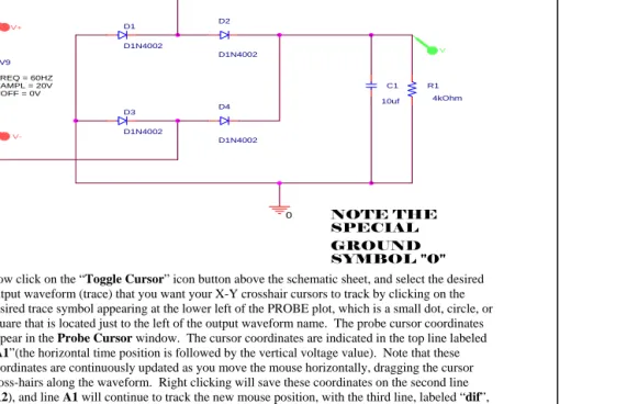
16.Now hit “P” to bring up the Place Part window again. This time, type “D” in the Part blank, in order to display the region of the parts list that contains the diode models, and choose the D1N4002 (1 A, 50 PIV power diode) part. Instantiate (place) this part 4 times on the schematic, and rotate the diodes into the standard bridge configuration (see Figure 1).
17.In similar fashion, place the resistor (R) and capacitor (C) as shown in Figure 1. Both of these components must have their component values entered (let R = 4KOhm and C = 10UF), since the default values shown are not the desired values. Double left click on these symbols, and enter the desired component values in the Property Editor; or double left click directly on the default value of each component, and enter the desired component value in the more compact “Display Properties” window. (This latter method is somewhat more convenient than the former. In fact, you could have entered the three VSIN parameters this way as well!)
18.To wire the parts together, click on Place – Wire, or simply hit the “W” key on the keyboard, or click on the Place Wire button icon (the third one from the top at the right of the screen). The mouse cursor changes from an arrow to a cross. Place the cross over a device terminal, then single click the left mouse button to connect a wire to this terminal, drag the wire to the terminal to which it is to be connected, and then single left click to connect the wire to this terminal. You may then repeat the procedure as many times as necessary, until all of the component terminals have been connected. A wire may be routed in a specific way by left clicking at intermediate points where you desire the wire to bend 90 degrees, thereby anchoring the wire to those intermediate points on the schematic grid. Notice that wires may cross without being connected to each other, just so you do not left click at the point where the wires cross!
19.To terminate wire entry, you may either right click and choose End Mode, or you may left click on the Selection (arrow) button icon, which is the topmost icon to the right of the schematic sheet. The cursor should change back from the cross to the selection arrow. The selection arrow may now be used to delete any misplaced wires, just as it was used above to delete or move schematic part symbols.
20.Before the schematic is complete, a ground reference symbol must be placed on one of the circuit nodes. Though many ground symbols are provided for drawing purposes, you must choose the one ground symbol whose name starts with the number “0”in order for the PSPICE simulation to work properly --- the “0” in the part name tells PSPICE that this is the ground node (Node 0). To bring up the ground symbols, hit the “G” key, or else click the GND icon button that appears to the right of the schematic sheet. In the Place Part Window that appears, the “0” ground may not initially be present. If it is not, click on the “Add Library” browse (if necessary) to the PSPICE directory, and select the “source” library. The “0” ground part should now be displayed. 21.Place the “0” ground symbol as shown in Fig. 1, and wire it to the indicated ground node. Of
course, multiple “0” ground symbols may be used to avoid having to tie all of the grounded nodes together with a wire.
22.We must tell PSPICE what output nodes are to be displayed in the PROBE plot. In this case, we are interested in plotting the voltage across the load resistor. Since one side of this resistor is grounded, we may use a “ended” probe (in much the same way that we would use a single-ended oscilloscope probe to view this voltage in the lab). Click on the single-single-ended voltage probe marker (circle V) icon at the top of the schematic sheet and deposit this probe to the top of the load resistor, as shown in Fig. 1. The other side of the voltage measurement is assumed to be the ground node.
23.Also of interest is the voltage across the VSIN source. Because neither side of this source is connected to the ground node, we must use a differential probe, just as we would have to use a pair of oscilloscope probes, to view the voltage across this source in the laboratory. Click on the differential voltage marker icon (circle + and circle -). Then deposit the (+) marker by single left clicking on the top terminal of the VSIN voltage source, and deposit the (–) marker by single left clicking a second time on the bottom terminal of the VSIN voltage source.
24.Labels may added to the schematic by clicking the ASCII entry icon labeled “A” (the bottom-most icon located to the right of the schematic sheet.)
25.Next we must tell Orcad how we want the transient PSPICE simulation to be carried out. This is done by creating a Simulation Profile by clicking on PSPICE – Create New Simulation Profile, or by clicking on the like-named icon at the top of the schematic sheet. Enter a name for this simulation profile (such as FW Rect), and hit the Enter key. A Simulation Settings window will appear. Select the “Time Domain (transient)” simulation type, and check the General Settings option. Change the Run To Time box to indicate how far in time we desire to run the transient analysis. Since in this simulation, our source is 60 Hz, and a 60 Hz sine wave repeats every 1/60 = 16.66 ms, we shall run our transient analysis out beyond 2 cycles = 34 ms. So enter 34MS into the Run To Time box, enter 0 into the “Start Saving Data After” box, and enter 50US into the Maximum Step Size box. (In general, the maximum step size should be about 1/1000 of the transient simulation run time.) Leave the Skip Initial Transient Bias Point Calculation box unchecked. Click OK.
Figure 1. Full-Wave Rectifier With C Filter – Drawn Using Orcad Lite
V
D4
D1N4002
V-NOTE THE SPECIAL D2
D1N4002
R1 4kOhm
0
GROUND SYMBOL "0" D1
D1N4002 V9
FREQ = 60HZ VAMPL = 20V VOFF = 0V
V+
D3 D1N4002
C1 10uf
27.Now click on the “Toggle Cursor” icon button above the schematic sheet, and select the desired output waveform (trace) that you want your X-Y crosshair cursors to track by clicking on the desired trace symbol appearing at the lower left of the PROBE plot, which is a small dot, circle, or square that is located just to the left of the output waveform name. The probe cursor coordinates appear in the Probe Cursor window. The cursor coordinates are indicated in the top line labeled “A1”(the horizontal time position is followed by the vertical voltage value). Note that these coordinates are continuously updated as you move the mouse horizontally, dragging the cursor cross-hairs along the waveform. Right clicking will save these coordinates on the second line (A2), and line A1 will continue to track the new mouse position, with the third line, labeled “dif”, registering the difference between the current cursor position A1 and the saved cursor position A2. The “dif” line permits easy measurement of output waveform slopes.
28.At any desired position of the cursor, you may permanently display the precise cursor coordinates right on the PROBE plot by clicking on the Mark Label button icon (located along the top, on the far right). Once the cursor crosshairs have been toggled off (by hitting the Toggle Cursor button a second time), you may use the mouse to drag the coordinate labels, and also the coordinate marking arrow, to a more readable position on the plot. Other cursor control icon buttons are available for automatically locating waveforms peaks and waveform troughs and positions of maximum slope --- these come in handy if we want to measure the ripple voltage amplitude of our full-wave rectifier circuit. In the PROBE plot of Fig. 2, I have used the appropriate buttons to automatically find the maximum (peak) and minimum (trough) output voltage excursions, and then I have used the Mark Label button to permanently label the coordinates of the peak and trough. These coordinates can be used to measure the simulated peak-to-peak output “ripple” voltage amplitude of 18.66 – 15.89 = 2.77 V.
29.Your plot may be labeled by clicking on the “ABC” text label button. Note that I have done this to label the plot “Full-Wave Rectifier with Capacitor Filter” in Fig. 2.
30.To print the schematic, first “select” the entire schematic, using your mouse to drag a rectangular selection box around the entire schematic diagram (highlighting it in violet-pink). To do this, position the mouse cursor in the upper left corner of the diagram, and then hold down the left
mouse button as you drag the cursor to the lower right corner of the schematic. Then release the left mouse button. Then select the “Scale to Paper Size” button, and click on File- Print - OK. 31.To copy and paste a schematic into an MSWORD document (such as a lab report), select the entire
schematic, and select Edit – Copy (Ctrl – C). Then in the Word document, position the cursor to the desired position and select Edit – Paste (Ctrl –V). Once the schematic appears in the WORD document, you may click on it to bring up the resizing bars. Also, if you right click on the schematic, then select Format Object – Layout – Tight, you will be able to drag the picture into the desired position.
32.The PROBE plot trace lines can be customized (color changed, assigned different dashed line patterns, or made thicker to stand out better) by right clicking on the desired trace and selecting Properties.
33.To print the PROBE plot, select the PROBE window and click on File – Print – OK. 34.To copy and paste a PROBE plot into an MSWORD document (such as a lab report), click on
Window – Copy to Clipboard, select the desired options (check the “Change White to Black” and the “Make Window and Plot Background Transparent” options), and then click OK. 35.To reopen an Orcad PSPICE simulation project at a later time, once it has been saved and you
have exited from PSPICE, you may use “My Computer” to browse to the project folder containing the project you wish to reopen, then click on the “.opj” Orcad Capture Project File Type icon in order to start Orcad PSPICE running that particular project. To display the schematic diagram for that project, click on the (+) symbol next to the “*.dsn” design file in the .opj project window to expand this entry. Then click on “Schematic 1” and finally click on “Page 1” to display the first page of the schematic.
Figure 2. Resulting Probe Plot for the Full-Wave Rectifier Circuit of Fig. 1
Time
0s 5ms 10ms 15ms 20ms 25ms 30ms 35ms
V(D2:2) V(D2:1,V1:-) -20V
-10V 0V 10V 20V
(29.158m,-19.991) (20.895m,19.980)
(29.363m,18.666)
(10.982m,15.893)
Full-Wave Rectifier with Capacitor Filter
R4
3k 668.8uA
R3
3k 668.8uA
V1 10Vdc
3.026mA
5.987V
R5 5k
1.529mA R2
2k 828.0uA
R6 4k
1.497mA
VW
0
VX
7.643V R1
1k 2.357mA
7.994V 10.00V
0V
VU R4
3k
0
R3
3k V1
10Vdc
R5 5k
R2 2k
I2
VU
R6 4k
VX R1
1k
I1
Open Circuit VW
I3
Example 2. DC (Bias Point) Analysis
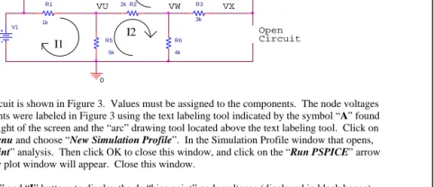
DC circuit analysis (finding the DC node voltages and element currents) in a circuit containing dc voltage and current sources and resistors can be performed by constructing a circuit diagram containing a number of resistors and one or more VDC constant voltage sources (battery symbol) or IDC constant current sources.
Figure 3. Example DC circuit to be analyzed
An example circuit is shown in Figure 3. Values must be assigned to the components. The node voltages and mesh currents were labeled in Figure 3 using the text labeling tool indicated by the symbol “A” found on the bottom right of the screen and the “arc” drawing tool located above the text labeling tool. Click on the PSPICE menu and choose “New Simulation Profile”. In the Simulation Profile window that opens, select “Bias Point” analysis. Then click OK to close this window, and click on the “Run PSPICE” arrow icon. An empty plot window will appear. Close this window.
[image:5.612.66.307.154.258.2]Click on the “V” and “I” buttons to display the dc “bias point” node voltages (displayed in black boxes) and element currents (displayed in red boxes) in the circuit, as shown in Figure 4. Note that the element currents are referenced entering the element terminal indicated by the dotted line. In some cases you may want to drag current label away from the element in order to see the dotted line more clearly, in order to know the side of the element that current is referenced as entering. Likewise, element voltages are referenced positive with respect to the terminal indicated by the dotted line. In some cases you will want to drag the voltage label away from the element in order to see the dotted line more clearly in order to know the side of the element at which the voltage is referenced positive.
Figure 4. Results of DC analysis after pressing the “V” and “I” buttons
The following MAPLE worksheet (Listing 1) verifies the result of the PSPICE simulation by performing both nodal analysis and mesh analysis to calculate the node voltages VU, VW, and VX in two different ways.
Listing 1. Maple Worksheet that predicts node voltages in the circuit of Fig. 3 using
both node voltage analysis and also mesh current analysis methods.
> restart;Example 1 Calculations
> r1:=1e3;r5:=5e3; r3:=3e3; r4:=3E3; r2:=2E3; r6:=4E3;
> neqn1:=(vu-10.)/r1+vu/r5+(vu-vw)/r2 = 0;
> neqn2:=(vw-vu)/r2+vw/r6+(vw-vx)/r3 = 0;
> neqn3:=(vx-vw)/r3+(vx-10.)/r4 = 0;
> solve({neqn1,neqn2,neqn3},{vu,vw,vx});
> mesheq1:=-10+(i1-i3)*r1+(i1-i2)*r5 = 0;
> mesheq2:=(i2-i1)*r5+(i2-i3)*r2+i2*r6 = 0;
> mesheq3:=(i3-i1)*r1+i3*r4+i3*r3+(i3-i2)*r2 = 0;
> solve({mesheq1,mesheq2,mesheq3},{i1,i2,i3});
Note the use of the assign statement below. It simply assigns the variables in the solve statement above to their corresponding solutions.
To prove this, I next display the newly assigned values of the variables i1, i2, and i3. > assign(%);
> vu := (i1-i2)*r5;
> vw:=i2*r6;
> vx:=10-i3*r4;
Note that the mesh equation results correspond to the node equation results, which in turn correspond to the PSPICE simulation results!
Example 3. Time Domain (Transient) Analysis
Consider the RC circuit shown in Figure 5. A pulse voltage source that is called “VPULSE” in the PSPICE parts menu is used in this example. VPULSE requires seven parameter values. In this example, VPULSE has been set up to change from V1 = 0 V up to V2 = 30 V after a delay time of TD = 0 seconds. The pulse rises in TR = 0 seconds and falls in TF = 0 seconds. It stays up at the V2 = 30 V level for PW = 1 second, and then falls back to the V1 = 0 V level for the rest of the period. It repeats this cycle every PER = 2 seconds. Note that two single-ended voltage probes have been placed at the input node (V1) and the output node (VC). These probes will cause the V1 and VC voltage waveforms to be displayed after the simulation has been run.
Figure 5. RC example circuit with pulse voltage source whose rising edge is used to
simulate a unit step input voltage, V1(t) = 30u(t) V.
0 R1
3k
VC
C1
10UF R4
6k
V V1
TD = 0
TF = 0 PW = 1sec PER = 2sec V1 = 0V
TR = 0 V2 = 30V
V
R3
6k R2
1k
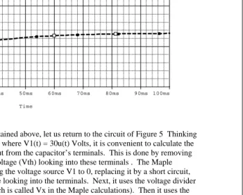
[image:6.612.437.728.128.268.2]The simulation profile must be set to the “Time Domain (Transient)” mode, with the “Run to” time set to a convenient stopping time, which you may have to discover by experiment (in this case, 0.1 seconds seems appropriate). The other boxes may be left blank. When the “Run PSPICE” arrow icon is pressed, and the simulation is complete, the probe plot shown in Figure 6 appears.
Figure 6. Resulting PROBE plot showing V1(t) and VC(t) node voltage waveforms
for just the rising edge portion of the VPULSE source, V1(t).
Time
0s 10ms 20ms 30ms 40ms 50ms 60ms 70ms 80ms 90ms 100ms V(R2:2) V(R1:1)
0V 10V 20V 30V
To verify the PSPICE simulation results obtained above, let us return to the circuit of Figure 5 Thinking of the V1(t) source as a step voltage source, where V1(t) = 30u(t) Volts, it is convenient to calculate the Thevenin Equivalent circuit seen looking out from the capacitor’s terminals. This is done by removing the capacitor and finding the open circuit voltage (Vth) looking into these terminals . The Maple worksheet of Listing 2 finds Rth by reducing the voltage source V1 to 0, replacing it by a short circuit, and then calculates the equivalent resistance looking into the terminals. Next, it uses the voltage divider equation to find the voltage across R2 (which is called Vx in the Maple calculations). Then it uses the voltage divider a second time to find the open circuit voltage across the terminals where the capacitor had been connected, which is the same as Vth. Thus, the capacitor sees a Thevenin Equivalent of Vth = 13.333u(t) volts in series with an Rth = 2 kohm resistor. Next, we may use the RC transient formula Vc(t) = Vf – (Vf – Vi)*exp(-t / tau), where Vf is the final voltage toward which the capacitor is charging (Vth), Vi is the initial voltage across the capacitor (0 V), and tau is Rth * C = 0.02 seconds. The resulting solution for the voltage across the capacitor is found to be
Vc(t) = 13.3333(1 – exp(-t/0.02)) Volts
The resulting MAPLE plot (Listing 2) matches the PSPICE Probe plot (Figure 6) precisely!
Listing 2. MAPLE Worksheet verifying simulation of the circuit of Fig. 5.
> Restart;> Rth:=(((R1*R3)/(R1+R3)+R2)*R4)/(((R1*R3)/(R1+R3)+R2)+R4);
> Rp:=((R2+R4)*R3)/((R2+R4)+R3);
> Vx:=30*u(t)*Rp/(Rp+R1);
> Vth:=Vx*(R4/(R2+R4));
> tau:=Rth*C1;
> Vc:=13.333 - (13.333 - 0)*exp(-t/(Rth*C1));
> plot(Vc,t=0..0.10);
Example 4. AC Sweep (Frequency response) Analysis
The circuit of Figure 7 is a “Double-Tuned Band Pass Filter” which passes sinusoids that fall within a narrow range of frequencies (called the passband), and does not pass sinusoids whose frequencies fall outside of this passband. We desire to PSPICE to simulate this circuit to plot the magnitude of the sinusoidal steady-state voltage gain, |Vout| / |Vin|, vs. frequency. The voltage source is a sinusoidal AC voltage source that is called “VAC” in the PSPICE parts menu. The amplitude of the sinusoidal voltage
Vout
C2
0.1uf
-V
-VX Vout
0
+
Vin 1VAC 0VDC
L1 10mh
1 2
C1 0.1uf R2
1k
L2 10mH
1 2 R1
1k
+
source, |Vin| has been set to 1 V, so that the plot of |Vout| vs. frequency will also indicate the voltage gain |Vout| / |Vin|.
Figure 7. Double-Tuned Band Pass Filter.
Notice that a voltage probe has been placed at the output of the filter so that the voltage gain will appear in the Probe Plot. In order to tell PSPICE to perform an AC sinusoidal steady-state frequency response simulation, the Simulation Profile must be set to “AC Sweep/Noise”. The AC Sweep Type was set to Linear, with a Start Frequency = 1 Hz (0 is not a permissible starting frequency), an End Frequency = 20,000 Hz, and Total Points = 100.
[image:7.612.42.407.75.464.2]The resulting Probe Plot is shown in Figure 8.
Figure 8. Probe Plot for the Double-Tuned Band Pass Filter of Figure 7.
Frequency
0Hz 2KHz 4KHz 6KHz 8KHz 10KHz 12KHz 14KHz 16KHz 18KHz20KHz V(C1:2)
0V 0.5V 1.0V
In order to make the resulting PROBE plot resemble a Bode frequency response plot (a plot of dB Gain vs. Log Freq), the Logarithmic radio button could have been checked, with Decade markings, as opposed to octave markings, selected.
Listing 3. MAPLE Analysis of the Double-Tuned Band Pass Filter
> > R1:=1E3;C1:=0.1E-6;L1:=10E-3;R2:=1E3;C2:=0.1E-6;L2:=10E-3;> neq1:=(Vx-1)/R1+Vx/(1/(I*2*Pi*f*C1))+Vx/(I*2*Pi*f*L1)+(Vx-Vout)/R2 = 0;
> neq2:=(Vout-Vx)/R2+Vout/(1/(I*2*Pi*f*C1))+Vout/(I*2*Pi*f*L2) = 0;
> solve({neq1,neq2},{Vout,Vx});
> assign(%);
> ResFreq := evalf(1/(2*Pi*sqrt(L1*C1)));
Example 5. Swept DC PSPICE Simulation
We often desire to obtain a dc voltage transfer curve (VTC) that relates a DC output voltage (Vout) to the swept DC input voltage (V1). Figure 9 shows the Orcad circuit of an asymmetrical diode voltage clipper circuit. To obtain the VTC of this circuit, place a voltage probe at the output voltage node.
Figure 9. Diode Clipper Circuit
R1
100Ohm
V2 -10V V1
1V
V Vout
V3 20V
D2 D1N4002
0
D1 D1N4002
R2
100kOhm
Now you must set up the Simulation Profile. In the Simulation Settings window’s Analysis Type box, choose the DC Sweep analysis type. Next, in the “Sweep Variable” section of the Simulation Settings window, you must identify one of the DC sources (in this example, V1) as the “Sweep Variable”. Even though V1 has been assigned a nominal voltage value (1 V), check the Voltage Source radio button, and in the Name box, enter the name of the desired DC source to be swept (V1). Then in the “Sweep Type” section of the Simulation Settings window, check the Linear radio button, and, supposing that we desire to sweep V1 from –30V to +30V, enter Start Value = -30V, End Value = +30V, and Increment = 0.1V. Then hit OK. Figure 10 shows the resulting VTC, we see that this circuit clips negative input voltage excursions at about –10.6 V, and positive input voltage excursions at about 20.6 V, as is easily predicted using elementary circuit theory.
Figure 10. Swept DC (VTC) Simulation of Diode Clipper Circuit
V_V1
-30V -20V -10V 0V 10V 20V 30V
V(D2:1) -20V
0V 20V 40V
(20.820,20.628)
(-10.810,-10.630)