Accepted Manuscript
Electron-terahertz interaction in dielectric-lined waveguide structures for electron manipulation
A.L. Healy, G. Burt, S.P. Jamison
PII: S0168-9002(18)30179-7
DOI: https://doi.org/10.1016/j.nima.2018.02.025
Reference: NIMA 60554
To appear in: Nuclear Inst. and Methods in Physics Research, A
Received date : 17 November 2017 Revised date : 25 January 2018 Accepted date : 5 February 2018
Please cite this article as: A.L. Healy, G. Burt, S.P. Jamison, Electron-terahertz interaction in dielectric-lined waveguide structures for electron manipulation,Nuclear Inst. and Methods in Physics Research, A(2018), https://doi.org/10.1016/j.nima.2018.02.025
Highlights
Reducing bandwidth of THz pulses maximises deflection
Corrugated waveguides are preferable to dielectric-lined waveguides for <10GHz bandwidth
pulses
Choice of electron injection time is important to maximise interaction with THz
Electron-Terahertz Interaction In Dielectric-Lined Waveguide Structures For Electron
Manipulation
A.L. Healya,b, G. Burta,b, S.P. Jamisonb,c
aDepartment of Engineering, Lancaster University, LA1 4YR, UK bThe Cockcroft Institute, Sci-Tech Daresbury, WA4 4AD, UK cAccelerator Science and Technology Centre, STFC, WA4 4AD, UK
Abstract
Terahertz-driven dielectric-lined waveguides (DLWs) have uses in electron manipulation; in particular deflection, acceleration, and focussing. A rectangular DLW has been optimised for deflection of 100 keV electrons using a THz pulse with a centre frequency 0.5 THz. Electron-THz interaction and the effect of electron bunch injection timing on maximising deflection is presented. DLWs
and corrugated waveguides are compared to discuss relative advantages and disadvantages.
Keywords: Terahertz, Dielectric, Electron manipulation
1. Introduction
1
Novel THz-driven structures are increasingly being consid-2
ered as alternatives to conventional radio frequency accelerat-3
ing structures due to potential for high accelerating gradients 4
[1, 2, 3]. Novel designs are also being explored for other uses 5
such as removing energy chirp, bunch deflection, and beam 6
diagnostics [4, 5, 6]. One promising design is the dielectric-7
lined waveguide (DLW). The use of cylindrical DLWs has been 8
demonstrated for acceleration, with an energy gain of 7 keV for 9
60 keV electron bunches [8]. The structure considered in this 10
work is a rectangular waveguide, with the longest sides each 11
lined with a layer of dielectric of equal thickness, as shown 12
in Figure 1. The addition of dielectric, which couples the 13
typical transverse electric and transverse magnetic modes to 14
generate hybrid modes, Longitudinal Section Electric/Magnetic
15
(LSM/LSE) [9], which for individual frequencies to propagate
16
with a phase velocity, vp, less than the speed of light,c. This
17
results in positive interaction of a monochromatic wave with 18
a propagating electron of velocity ve = vp, which is
indef-19
inite when there is no longitudinal acceleration. For deflec-20
tion and acceleration, modes LSM01 and LSM11 respectively
21
are excited. The polarization and spatial profile of the exter-22
nal field dictates the excited mode and therefore the effect of
23
the DLW on a particle bunch, in this case electrons. For the 24
purpose of this investigation the structure was considered for 25
deflection only but it can also support accelerating modes. In 26
this paper DLW design is discussed, and a general overview 27
of THz-electron interaction in waveguide structures is provided 28
with regards to interaction length. The analysis of interaction 29
length and dispersion is valid for all structures in which the dis-30
persion relation is modified such thatvp = vefor at least one
31
Email address:[email protected]()
1Work supported by the STFC core grant ST/K520133/1
frequency, providedveremains constant. Coupling and its
ef-32
fects are ignored in this analysis. The effect of THz pulse length
33
is demonstrated for the specific example of a DLW operating at 34
0.5 THz and designed to deflect 100 keV electrons, matching 35
the energy of an existing electron gun. Future structures will 36
be focussed on fully relativistic beams at the CLARA facility at 37
STFC Daresbury Laboratory [10]. A comparison of DLWs and 38
corrugated waveguides is presented with a focus on interaction 39
length. Transverse deflecting structures have uses in
diagnos-Figure 1: Cross-sectional view of the dielectric-lined waveguide, showing the LSM01mode profile. Left: cross-sectional side view, right: entrance view. The
waveguide is a rectangular metallic waveguide with two identical quartz slabs loaded on the top and bottom.
40
tics; a time-dependent deflection of a bunch is projected onto a 41
screen, converting longitudinal position to transverse position. 42
2. DLW design
43
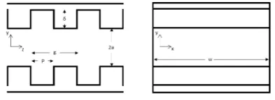
We consider a waveguide of lengthLwith dimensions given bya,b, and w, where ais the half vacuum aperture,b =a+ δ, whereδis the dielectric thickness, andwis the waveguide width. The presence of the dielectric modifies the waveguide dispersion relation from that of a hollow rectangular waveguide [11];
kb y,mntan
kb
y,mn(b−a)
=rkay,mncot
ka
y,mna
, (1)
form=1,3, . . ., corresponding to a maximal longitudinal axial
electric fieldEz,0. Form=0,2, . . ., corresponding toEz,0 =0,
Preprint submitted to Nuclear Instruments and Methods A January 25, 2018
*Manuscript
[image:3.595.330.531.459.526.2]the dispersion relation is given by
kby,mntan
kby,mn(b−a)
=−rkay,mntan
kay,mna
, (2)
where r is the relative permittivity of the dielectric. The
wavenumbers directed along the stratification are given by
ka y,mn=
r k2 0− mπ w 2
−βmn, (3)
kb y,mn=
r
rk20−mπ
w 2
−βmn, (4)
in the vacuum aperture and dielectric respectively. βmn is the
44
longitudinal wavenumber. Equations (1) and (2) must be solved 45
numerically to findβmnand thus the dispersion relation. The
46
choice of DLW geometry depends on the electron bunch di-47
mensions, electron energy and type of interaction required. The 48
vacuum aperture was limited to a minimum of 200 µm, dou-49
ble the transverse beam size of the planned interaction point. 50
Quartz was selected as the dielectric due its availability and 51
low loss tangent [12]. w, a, and δ were chosen by analysis
52
of the effects of each parameter on the interacting bandwidth
53
and axial voltage. It was found that matching bandwidth and 54
maximising field was not possible; a compromise between the 55
two was reached. Waveguide parameters were inserted into the 56
dispersion relation which was solved analytically. Properties 57
of the DLW such as field components were then analytically 58
obtained from the calculated wavenumbers [11], assuming the 59
input power of each frequency is constant. 60
3. Interaction length
61
The operating frequency fop is defined as that at which the
phase velocityvpis equal to the longitudinal electron velocity,
ve. A monochromatic THz field at this frequency will propagate
indefinitely with an electron without phase slippage. An elec-tron will slip out of phase with a frequency other than fopover
the length of the structure asvp ,ve. Provided phase slippage
is less than±π/2 respectively, the interaction will be entirely positive, giving theinteracting bandwidthconstraint
|β(ω)−βe(ω)|L≤π
2 , (5)
whereβ(ω)= ω/vp(ω) is the longitudinal wavenumber,βe =
ω/veandLis the structure length. Evaluating Equation (5) at
ω1 andω2, the frequencies at which phase slippage is ±π/2
respectively and subtracting
β(ω2)−β(ω1)−(ω2v−ω1)
e
!
Lint=π , (6)
giving an effective bandwidth of
∆f =ω2−ω1
2π =
1
2πve β(ω2)−β(ω1)+ π Lint,p
!
. (7)
This can be rearranged to get the interaction lengthLint,p for a
given input THz pulse bandwidth, assuming that all frequencies
are in phase at the start of the waveguide. Outside of this length, the edge frequencies interact negatively with the propagating electron. An alternative definition of the interaction length can be obtained by considering the slippage of the electron from the pulse envelope. For a transform-limited Gaussian pulse, which has the shortest pulse duration for a given optical spectrum, the time-bandwidth product isτ∆f ≤0.44. The interaction length, Lint,g, is calculated [13] using
∆f = 0.44
Lint,g
1
vg− 1
ve
, (8)
assumingvgis frequency independent. It must be emphasised
62
that both equations are approximations; Equation (7) only con-63
siders individual frequencies, not a real pulse, and Equation (8) 64
assumes no group velocity dispersion. 65
4. THz-electron interaction
66
The THz-electron interaction was simulated using the CST 67
Particle-in-Cell (PIC) solver [14]. Two THz pulses were inves-68
tigated; a single-cycle Gaussian with bandwidth 0-1 THz and 69
a ten-cycle pulse with bandwidth 0.3-0.7 THz, corresponding 70
to planned experimental parameters. A 73 ps bunch of on-71
axis probe particles with no initial transverse emittance was 72
launched to co-propagate with the THz pulse; only single par-73
ticle dynamics were considered. Each pulse was launched di-74
rectly into the LSM01 mode. Figure 2 shows the normalised
75
axialEyfield of the two pulses just after launch and after
prop-76
agating 10 mm into the waveguide. The input power of the 77
THz pulse across the input face of the waveguide is the same 78
in both cases. The single-cycle pulse was highly dispersed by 79
waveguide propagation and the maximum amplitude decreased 80
as a result, whereas the shape of the 10-cycle pulse remained 81
largely unchanged. The effect of the two THz pulses on
inter-82
acting electrons with different injection times is shown in
Fig-83
ure 3. The interaction with a ten-cycle pulse is shown in Figure 84
3b. An electron injected with the front of the pulse, such as that 85
tracked to ‘Peak 2’, slips out of the pulse asvg ,veand so has
86
a lower y-momentum gain than ‘Peak 1’, corresponding to the 87
electron with maximal gain. This was injected towards the end 88
of the THz pulse on a peak. Electrons on ‘Peak 1’ and ‘Peak 89
3’ are still interacting as they have not propagated completely 90
through the pulse by the end of the structure. Therefore a 10-91
cycle pulse would provide a greater maximum interaction given 92
a longer structure.In the case of a single-cycle pulse, electrons 93
injected just behind the trailing edge of the single-cycle pulse 94
are given the largest kick iny, corresponding to ‘Peak 1’ in Fig-95
ure 3a. Later electrons, such as those with a final energy cor-96
responding to ‘Peak 2’ and ‘Peak 3’ experience less of a kick. 97
The three particles selected for investigation leave the 10 mm 98
structure with maximised net deflection but experience a peri-99
odic variation in interaction as a result of pulse dispersion. The 100
periodicity is approximately 0.02 ns, with a positive interaction 101
over 0.01 ns, corresponding to a length of 1.6 mm. From Equa-102
tion (7), the interaction length should be≈700µm. The sim-103
ulated interaction is more than doubled for an electron injected 104
0 mm 10 mm
0.00 0.05 0.10 0.15 0.20
-0.4
-0.2
0.0 0.2 0.4 0.6 0.8 1.0
Time[ns}
Normalised
amplitude
[
V
/
m
]
(a)
0 mm 10 mm
0.00 0.05 0.10 0.15 0.20
-1.0 -0.5 0.0 0.5 1.0
Time[ns]
Normalised
amplitude
[
V
/
m
]
[image:5.595.64.535.71.227.2](b)
Figure 2: Dispersion of a THz pulse due to DLW. The amplitude ofEyfield on-axis is measured as a function of time. a) single-cycle THz pulse, b) ten-cycle THz pulse. The input power of the THz pulse across the input face of the waveguide is the same in both cases. And the amplitude is normalised to the input single-cycle pulse.
Peak 1 Peak 2 Peak 3
0.00 0.02 0.04 0.06 0.08 0.10
-0.004 -0.002
0.000 0.002 0.004 0.006
t[ns] py
[
βγ
]
(a)
Peak 1 Peak 2 Peak 3
0.00 0.02 0.04 0.06 0.08 0.10
-0.004
-0.002
0.000 0.002 0.004
t[ns] py
[
βγ
]
[image:5.595.61.536.263.417.2](b)
Figure 3: Grey: Momentum kick experienced by on-axis electrons due to interaction with a THz pulse as a function of injection time at the end of the 10 mm structure. Black, blue, red: following a single electron on a momentum peak from start to end of the waveguide. a) single-cycle THz pulse, b) ten-cycle THz pulse.
with the peak of the THz pulse. This suggests that our defini-105
tion of interaction length is an underestimate as the interaction 106
of the central frequencies in the bandwidth is not cancelled out 107
by the edge frequencies. It is therefore preferable to minimise 108
dispersion, which is achieved via the use of a narrowband THz 109
pulse, although practically this is at the expense of THz power 110
as narrowband sources are typically less efficient than
broad-111
band sources. 112
5. Comparison to corrugated waveguides
113
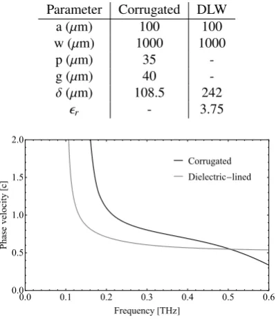
A corrugated rectangular metallic waveguide, such as shown in Figure 4, is a simple alternative to the DLW. It is similar to a conventional iris-loaded cavity in that longitudinal variation in the aperture serves to modify the dispersion relation from that of a metallic rectangular waveguide. The dispersion rela-tion and electromagnetic fields were calculated using CST Mi-crowave Studio (MWS). A comparison between the two struc-ture types was performed for a strucstruc-ture optimized to deflect 100 keV electrons, primarily by assessing the phase and group velocity and the transverse voltage,
Vy(ω)=
Z L
0
Ey(ω)+veBx(ω)
exp
"
−i β(ω)z−vω
ez
!#
dz,
(9)
Figure 4: Cross-sectional view of the corrugated waveguide. Left: side view, right: entrance view. The waveguide is a rectangular metallic waveguide with periodic corrugations on the top and bottom.
where only theydirection is considered as there is no axial field 114
acting inx. The electron velocity is included to account for the 115
variation ofvpwith frequency, asvp =ω/β(ω). The optimised
116
structure dimensions are shown in Table 1 for an operating fre-117
quency fop =0.5 THz and electron energy 100 keV. Figures 5
118
and 6 show that the DLW is less dispersive than the corrugated 119
waveguide as bothvpandvgvary less close to fop. In both cases
120
vg<vefor all frequencies and so the pulse envelope propagates
121
slower than the electron bunch, limiting the interaction length. 122
Using Equation (7), a corrugated structure of length 10 mm re-123
quires a input THz bandwidth less than 5.2 GHz for monotonic 124
interaction, whereas Equation (8) estimates 4.7 GHz, with the 125
discrepancy arising due to assumptions in both equations. For 126
[image:5.595.328.525.470.542.2]Table 1: Parameters of the optimised corrugated and dielectric-lined waveg-uides. Parameters are defined in Figure 4.
Parameter Corrugated DLW
a (µm) 100 100
w (µm) 1000 1000
p (µm) 35
-g (µm) 40
-δ(µm) 108.5 242
r - 3.75
Corrugated Dielectric-lined
0.0 0.1 0.2 0.3 0.4 0.5 0.6
0.0 0.5 1.0 1.5 2.0 Frequency[THz] Phase velocity [ c ]
Figure 5: Phase velocity of the corrugated waveguide and DLW as a function of frequency. The crossing point at 0.5 THz is whenvp=ve.
the DLW, Equations (7) and (8) give∆f of 70 GHz and 62 GHz 127
respectively. Figure 7 shows the transverse voltageVyin both
128
cases, calculated using data taken from CST for individual fre-129
quencies, assuming power of each frequency is constant, and 130
inserted into Equation (9). The corrugated waveguide has a 131
higherVyat the centre frequency than the DLW, butVyfor other
132
frequencies is lower and periodicity of variation is shorter. Fig-133
ure 8 shows Vy integrated over a given frequency range ∆ω,
134
Vint y =
Rω0−∆ω/2
ω0+∆ω/2 Vy(ω), assuming a constant spectral
distribu-135
tion and centred onω0. With increasing bandwidth, the power
136
of the pulse increases. This shows that the use of a DLW is 137
favourable except for bandwidths less than∼50 GHz. Despite 138
the larger maximumVyof the corrugated waveguide, integrated
139
voltage is smaller as a result of the largervp,vgvariation. The
140
bandwidth corresponding to maximumVywas 9.3 GHz for the
141
corrugated waveguide and 132 GHz for the DLW. The approxi-142
mations made in Equations (7, 8) are therefore not valid in this 143
analysis. 144
6. Conclusions
145
A DLW structure, designed to deflect 100 keV electrons, has 146
been investigated and compared with a corrugated waveguide. 147
The effect of THz pulse bandwidth on magnitude of transverse
148
deflection has been numerically investigated and it has been es-149
tablished that choice of THz pulse bandwidth is important to 150
maximise deflection. If bandwidth is too small, an electron will 151
not pass through the entire pulse and so will not experience 152
maximum possible deflection. A THz pulse with a large band-153
width is dispersed and the pulse peaks do not propagate with the 154
same velocity as the electron, resulting in variation of transverse 155
kick direction. The ideal pulse bandwidth results in an electron 156
Corrugated Dielectric-lined
0.0 0.1 0.2 0.3 0.4 0.5 0.6
0.0 0.1 0.2 0.3 0.4 0.5 0.6 Frequency[THz] Group velocity [ c ]
Figure 6: Group velocity of the corrugated waveguide and DLW as a function of frequency. Neither waveguide achievesvg =veat 0.5 THz, necessary for
indefinite interaction.
Dielectric-lined Corrugated
0.35 0.40 0.45 0.50 0.55 0.60 0.65
-0.2 0.0 0.2 0.4 0.6 0.8 1.0
Frequency[THz]
Transverse voltage [ A .U ]
Figure 7: Transverse voltageVyof the corrugated waveguide and DLW as a
function of frequency, normalised to DLW maximum. The power is the same for each input frequency.
passing through the entire pulse over the length of the structure, 157
starting at the trailing edge of the pulse and exiting the waveg-158
uide just ahead of the leading edge. For the corrugated waveg-159
uide considered here, the large dispersion leads to a requirement 160
of a 9.3 GHz pulse bandwidth compared to the 132 GHz band-161
width of the DLW over a 10 mm structure. The higher peak 162
field strengths achievable with short broadband THz pulses, to-163
gether with increased efficiency of non-linear generation, leads
164
to more favourable conditions for DLW structures. Future ex-165
perimental work will investigate this. Inclusion of group veloc-166
ity dispersion and higher-order effects will be included in future
167
work by time-domain analysis of THz-electron interaction, thus 168
investigating the effect of real THz pulses.
169
Dielectric-lined
Corrugated
0 50 100 150 200 250 300
0.0 0.2 0.4 0.6 0.8 1.0
Frequency[THz]
[image:6.595.64.264.101.332.2]Integrated transverse voltage [ A .U ]
Figure 8: Transverse voltageVyof the corrugated waveguide and DLW,
inte-grated over a given bandwidth and normalised to the DLW maximum value. The power spectrum over each bandwidth is constant.
[image:6.595.331.532.597.728.2][1] England, R.J. et al., ”Dielectric laser accelerators”,Reviews of Modern
170
Physics, 2014 (86) 171
[2] Hebling, J., et al., ”Optical manipulation of rela-172
tivistic electron beams using THz pulses”, preprint at 173
https://arxiv.org/ftp/arxiv/papers/1109/1109.6852, 2011 174
[3] Walsh, D.A. et al., ”Demonstration of sub-luminal propagation of single-175
cycle terahertz pulses for particle acceleration”,Nature Communications, 176
2017 (8) 177
[4] Fu, F. et al., ”Demonstration of nonlinear-energy-spread compensation in 178
relativistic electron bunches with corrugated structures”,Physical Review
179
Letters, 2015 (114) 180
[5] Pacey, T.H. et al., ”Phase space manipulation of sub-picosecond electron 181
bunches using dielectric wakefield structures”,Proceedings of IPAC2017, 182
2017 183
[6] Bettoni, S., et al, ”Temporal profile measurements of relativistic electron 184
bunch based on wakefield generation”,Physical Review Accelerators and
185
Beams, 2016 (19) 186
[7] Dexter, A.C. et al., ”CLIC crab cavity design optimisation for maximum 187
luminosity”,Nuclear Instruments and Methods in Physics Research A,
188
2011 (657)
189
[8] Nanni,E.A. et al., ”Terahertz-driven linear electron acceleration”,Nature
190
Communications, 2015 (6) 191
[9] Collin, R.E., ”Field Theory of Guided Waves”, Wiley-IEEE Press, 1960 192
[10] Clarke, J.A. et al., ”CLARA conceptual design report”,Journal of
Instru-193
mentation, 2014 (9) 194
[11] Xiao, L. et al., ”Field analysis of a dielectric-loaded rectangular waveg-195
uide accelerating structure”,Physical Review E, 2001 (65) 196
[12] Hejase, J.A., et al, ”Terahertz characterisation of dielectric substrates 197
for component design and nondestructive evaluation of packages”,IEEE
198
Transactions on Components, Packaging and Manufacturing Technology, 199
2011 (11) 200
[13] Healy, A.L. et al., ”Group velocity matching in dielectric-lined waveg-201
uides and its role in electron-terahertz interaction”, Proceedings of
202
IPAC’17, Copenhagen, Denmark, 2017 203
[14] <https://www.cst.com/ >
204
[15] Carbajo, S. et al., ”Efficient narrowband terahertz generation in cryogeni-205
cally cooled periodically poled lithium niobate”Optics Letters, 2015 (40) 206