Integrated Optical Components for
Quantum Key Distribution
Yasir Jamal Noori
Department of Physics
Lancaster University
This thesis is submitted in partial fulfilment of the requirements for the
degree of Doctor of Philosophy
i
Declaration
I declare that this thesis, unless stated otherwise, is the result of my own work which I carried out in
Lancaster University between September 2013 and August 2016. To the best of my knowledge and
belief, it contains no material previously published or produced by another party in fulfilment, partial
or otherwise, of any other degree or diploma at another university or institute of higher learning, except
where due acknowledgement and reference is made in the text. This thesis is not the same as any others
I have already submitted, or in the process of submitting, for any degree at any university or institution.
The word count on this thesis does not exceed the maximum limit of 80,000 words.
ii
Acknowledgements
I would first and foremost like to direct my sincere appreciation and gratitude to my supervisor, Robert
J Young, for his excellent supervision and invaluable support and guidance throughout the period of
my PhD. His great passion and motives for research has and continues to fuel that of mine. I would like
to thank him for giving me the opportunity to be part of his research project, many thanks for all the
fascinating projects he offered and for the freedom I was given during my work. Rob has helped
defining the researcher I am today and I do not doubt that without him, this project would not have been
possible.
I would like to thank my second supervisor Utz Roedig for supervising my work from the computer
science side and for being always ready to give me the support and guidance when I needed him. A lot
of gratitude to Phillip Speed for being first a great friend and secondly a very wise business partner,
who can always boost my energy to let me provide more for the sake of my research and future career.
I’ve been very lucky to have had the chance to work with a number of amazing people during my studies
in Lancaster University. The friendship I developed with Yameng, Jonny, Chris, Ramon, Ethem and
Matt have been very effective in reducing the pressure that I could have otherwise faced without them
from working hard during my PhD. I feel very happy to have been easily able to blend in well with
them despite the cultural and language barriers.
A lot of thanking goes to Andrew R J Marshall and Aiyeshah Alhodaib for growing the InAs nanowires,
Peter Hodgson for growing the GaSb quantum dots, Yuri Pashkin, Atif Aziz and Richard George for
giving me the trainings I needed in the Quantum Technology Centre and the invaluable experimental
support and discussions that have helped me with my work.
My parents Nada and Jamal, my siblings Dhafer and Rania and my love Dania, I could have never have
reached anywhere close to where I am now without your love, support and constant encouragements.
Thank you for teaching me to believe in myself and in my dreams. I have and will always try to make
you proud. I love you all.
To my current and previous house mates, Maysara, Kabeer, Mohammad, Sharih, Ahmed and Iznan, the
joyful time I spend with you every night after a long day of work has been very effective at clearing my
head from work matters and keeping my stress levels down.
Finally, I extend my gratitude to the faculty of Science and Technology for funding me throughout my
iii
List of publications
1. J. R. Orchard, C. Woodhead, J. Wu, M. Tang, R. Beanland, Y. J. Noori, H. Liu, R. J. Young, D. J. Mowbray, “Silicon-based single quantum dot emission in the telecoms C-band” ACS Photonics, 4, 1740-1746 (2017)
2. C. S. Woodhead, J. Roberts, Y. J. Noori, Y. Cao, R. Bernardo-Gavito, P. Tovee, A. Kozikov, K. Novoselov and R. J. Young, “Light extraction from 2D materials using liquid formed micro-lenses” IOP 2D Materials, 4, 015032 (2016)
3. Y. J. Noori, Y. Cao, J. Roberts, C. S. Woodhead, R. Bernardo-Gavito, P. Tovee and R. J. Young, “Photonic crystals for enhanced light extraction from 2D materials” ACS Photonics, 3, 2515-2520 (2016)
4. J. Roberts, I. E. Bagci, M. A. M. Zawawi, J. Sexton, N. Hulbert, Y. J. Noori, C. S. Woodhead, M. Missous, M. A. Migliorato, U. Roedig and R. J. Young, “Atomic-scale authentication with resonant tunnelling diodes” MRS Advances 1, 1625 (2016)
5. J. Roberts, I. E. Bagci, M. A. Zawawi, J.Sexton, N.Hulbert, Y. J. Noori, M. P. Young, C. S. Woodhead, M. Missous, M. A. Migilorato, U. Roedig and R. J. Young, “Using quantum confinement to uniquely identify devices” Nature Sci. Rep. 5, 16456 (2015)
6. M. P. Young, C. S. Woodhead, J. Roberts, Y. J. Noori, M. T. Noble, A. Krier, E. P. Smakman, P. M. Koenraad, M. Hayne and R. J. Young, “Photoluminescence studies of individual and few GaSb/GaAs quantum rings” AIP Advances 4, 117128 (2014)
7. R. Bernardo-Gavito, J. Roberts, J. Sexton, B. Astbury, H. Shokeir, T. McGrath, Y. J. Noori, C. S. Woodhead, M. Missous, U. Roedig, R. J. Young, “Extracting random numbers from quantum tunnelling through a single diode” arXiv:1706.07348 (Manuscript submitted to Nature Electronics, 2017)
8. Y. Cao, A. J. Robson, A. Alharbi, J. Roberts, C. S. Woodhead, Y. J. Noori, R. Bernardo-Gavito, D. Shahrjerdi, U. Roedig, V. I. Fal’ko, R. J. Young, “Optical identification using imperfections in 2D materials” arXiv:1706.07949 (Accepted for publishing in IOP 2D Materials, 2017)
9. Y. J. Noori, R. J. Young. “A photonic device” GB1706216.7 (18 July 2017)
iv
Abstract
The security of current public key cryptosystems, such as RSA, depends on the difficulty of computing
certain functions known as trapdoor functions. However, as computational resources become more
abundant with the fast development of super- and quantum computers, relying on such methods for
communication security becomes risky. Quantum key distribution (QKD), is a potential solution that
can allow theoretically secure key exchange for future communications. Chip-scale integration of this
solution for securing communication of embedded systems and hand held devices demands
miniaturizing the optical components that are used in typical QKD boxes, hence reducing its size and
cost. The aim of the work in this thesis is firstly investigating novel approaches to realising integrable
single photon sources and detectors for applications such as QKD, and secondly proposing a chip-scale
integrated QKD system with efficient and optimised optical components.
In the first part of the thesis, a model for coupling 2D material emitters to rod-type photonic cavities is
studied for room temperature single photon sources. Our investigated approach allows better coupling
between the emitter and the cavity modes than conventional methods, while increasing light collection
ratio. In the second part, site-controlled growth of semiconductor III-V nanowires on Si for
photodetection applications is achieved by fabricating the sites using electron-beam lithography and
wet etching. Studies were also carried out to investigate the effect of the wafer’s growth temperature on
the nanowire formation. Finally, a model was proposed for realising a chip-scale QKD system using
photonic crystals as a photonic circuit platform. The work involves increasing the Q-factor of the cavity
single photon source, increasing cavity waveguide coupling, reducing losses in beam splitters and
out-couplers. A final model of a chip-scale QKD system which involves the optimised components is
v
Table of Contents
Chapter 1 ... 1-1
Classical Key Sharing Schemes ... 1-1
Quantum Cryptography for Secure Key Sharing ... 1-3
Practical Challenges in QKD ... 1-6
Thesis Outline ... 1-8
Bibliography ... 1-11
Chapter 2 ... 2-1
Semiconductors and Quantum Dots ... 2-1
2.1.2. Self-Assembled Quantum Dots ... 2-3
2.1.3. Defects in 2D Materials ... 2-3
Photonic Crystals ... 2-4
2.2.1. Photonic Band Structure ... 2-4
2.2.2. Photonic Crystal Resonators and Waveguides ... 2-6
2.2.3. Purcell Enhancement ... 2-10
Single Photon Detectors ... 2-12
2.3.1. P-I-N Junctions ... 2-13
2.3.2. Avalanche Multiplication ... 2-14
Differential Phase QKD Protocols ... 2-15
Bibliography ... 2-19
Chapter 3 ... 3-1
Introduction ... 3-1
Fabrication Techniques ... 3-2
3.2.1. Electron-Beam Lithography ... 3-2
3.2.2. Thermal (Resistive) Evaporation ... 3-7
3.2.3. Lift-Off ... 3-7
3.2.4. Molecular Beam Epitaxy ... 3-9
3.2.5. Etching ... 3-9
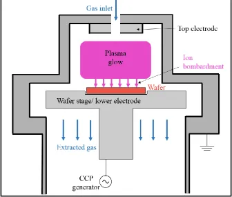
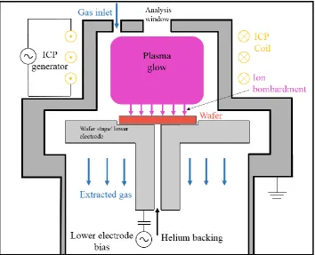
3.2.6. RIE and RIE-ICP ... 3-11
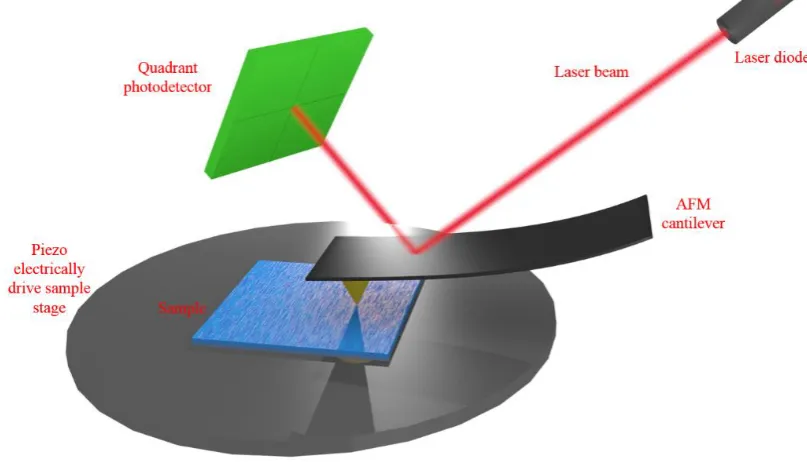
Scanning Probe Microscopy ... 3-14
Fabrication of Hole-Type Photonic Crystals... 3-16
Numerical Modelling With Finite Difference Time Domain... 3-22
Micro-Photoluminescence Spectroscopy ... 3-25
vi
Chapter 4 ... 4-1
Introduction ... 4-1
TMDC Monolayers as Quantum Light Emitters ... 4-2
Cavity Fabrication and Emitter Transfer ... 4-11
Conclusions ... 4-17
Bibliography ... 4-19
Chapter 5 ... 5-1
Introduction ... 5-1
Site-Controlled Nanowire Fabrication ... 5-6
InAs and GaAs Nanowire Growth ... 5-9
Conclusion ... 5-20
Bibliography ... 5-21
Chapter 6 ... 6-1
Introduction ... 6-1
6.1.1. Motivation ... 6-2
6.1.2. GaAs as an Optoelectronic Material for QKD ... 6-3
Components for QKD ... 6-5
6.2.1. Single Photon Cavity for QKD ... 6-5
6.2.2. Integrated Waveguides for QKD ... 6-7
6.2.3. Photon Out-Coupling for a QKD Chip ... 6-10
Numerical Optimisation of QKD Components ... 6-11
6.3.1. Optimising Cavity Confinement for Single Photon Emission ... 6-11
6.3.2. Optimising Waveguide-Cavity Coupling for Efficient Beam splitting ... 6-16
6.3.3. Y junction Photonic Crystal Beam splitters for Integrated QKD Systems ... 6-19
6.3.4. Optimised Light Out-Coupling Efficiency from a Photonic Crystal Waveguide ... 6-20
Assembling a Chip-Scale QKD System ... 6-23
Preliminary Experimental Results for Photonic Crystals Using GaSb QDs ... 6-23
Conclusions ... 6-26
Bibliography ... 6-28
Chapter 7 ... 7-1
Conclusions ... 7-1
Future Work ... 7-6
Chapter 1 – Introduction
1-1
Chapter 1
Introduction
Classical Key Sharing Schemes
Since the advent of the Internet, continuous development in its security has been a major challenge for
researchers and industrial organisations that specialise in this field. Today, the importance of the
Internet’s security is not solely based on its usage for social media or online shopping, but if it were to
be breached by attackers, human lives could be put in danger and many modern countries’ national
securities could become vulnerable. This has always been a driving motivation to further research and
develop the security of communication systems. An example of the serious importance of network and
Internet security is its involvement in online voting and crisis management. In the present day, the
internet is used extensively for national economy control and simultaneously for the resolution of
military tasks. These sensitive uses of the Internet make its security an essential goal that needs to be
achieved at all times.
Today, when valuable data such as credit card numbers are sent to an online store for a payment, public
key cryptography protocols such as Transport Layer Security (TLS) are used to authenticate the store’s
server1. After the authentication, TLS is used to negotiate a symmetric session key, which can later be
used for encrypting data, such as the credit card’s number, transferred between the two parties. This
process is also known as key exchange/distribution/negotiation/establishment. The exchanged key can
Chapter 1 – Introduction
1-2
entirely on the key and the encryption scheme. If a secure encryption scheme was used, in combination
with a secret key, the only way for an eavesdropper to have knowledge about the transmitted
information is through knowing the key used for encryption. Hence, firstly, the key exchange
mechanism used for sensitive applications should be ultimately secure to prevent eavesdroppers from
obtaining any information about the key. Secondly, the key should be used with a provably uncrackable
encryption technique such as the one-time pad. This will prevent an eavesdropper from obtaining any
information about the message if the key exchange and encryption are executed correctly.
Common existent techniques of key exchange between multiple parties depend on what's known by
mathematicians and cryptographers as trapdoor functions. RSA is a popular protocol that exploits
trapdoor functions to allow key exchange. The security of RSA for key exchange relies on the
assumption that it is computationally infeasible to factorise a large number into its prime factors. If an
eavesdropper, Eve, can listen to what is sent across a communication channel during an RSA protocol
between a sender, Alice, and a receiver, Bob, then she should be able to decrypt the cipher using just
Bob’s publicly revealed key, but only if she has enough computational power. If that was the case, Eve
would be able to decrypt the cipher and recover the symmetric key. In other words, current cryptography
systems that use RSA and complexity related schemes for key exchange are vulnerable if an attacker
were to have access to high computational resources, making one way functions reversible.
This security scheme, to some extent is a temporary solution. The constant development of super and
quantum computers can lead to faster and more efficient breaking of RSA schemes by eavesdroppers
who have access to such technology. Although the latter is not yet a reality, the basic principles have
been proven in laboratories and theoretically have been shown to be especially capable for computing
complex mathematical equations such as trapdoor functions2, 3. If such computation capabilities are
achieved, a future adversary could break the encryption of many communication channels that depend
on RSA for their security, introducing a retroactive vulnerability overnight. One of the theories that was
published and led to an increase in security development efforts was Shor’s algorithm for quantum
Chapter 1 – Introduction
1-3
time by using a quantum computer. This led to a great increase in research efforts in this field after
1994. Since then, researchers have been pushing the limits of data transfer rates and the maximum
achievable communication distances using quantum phenomena-based provably secure systems.
Quantum Cryptography for Secure Key Sharing
Provably secure systems use quantum mechanical principles for securing communication, this is
commonly known as quantum key distribution (QKD). QKD prevents an eavesdropper from listening
to the QKD channel without being discovered using the unbreakable fundamental laws of physics. This
sets upper bounds on the amount of knowledge that Eve can obtain about the transferred data between
Alice and Bob.
Like classical key distribution methods, QKD is also not immune against active man in the middle
attacks. Thus, prior to Alice and Bob using QKD as a key distribution protocol, they need to have an
authenticated quantum and classical channel. This ensures they do not succumb to an active man in the
middle attack. This means a seed key is needed prior to starting the QKD scheme, to be used by Alice
and Bob to authenticate each other. For this reason, QKD is often referred to as a key growing protocol.
The first QKD protocol, BB84, was proposed by Bennett and Brassard in 1984, and since then several
recognised security proofs have been reported to prove its security4, 5. The protocol begins with Alice
preparing her random digital key that she would like to share with Bob. Next, Alice and Bob agree on
different polarisation bases for bit encoding. For example, in the rectilinear basis, Alice and Bob can
use vertically and horizontally polarised photons to represent 0 and 1, respectively. On the other hand,
they represent 0 and 1 using photons polarised at 45 and 135 degrees in the diagonal basis. In sending
these bits, Alice uses a trusted random number generator (RNG) to make her choice for the basis she
uses for encoding each qubit on each photon pulse, before sending the pulses to Bob for measurements.
On receiving the qubits, Bob also performs his measurements using a random number generator to make
Chapter 1 – Introduction
1-4
Following the measurements stage, Alice and Bob publicly broadcast their chosen encoding basis and
measurement basis for every single qubit. A comparison session between the encoding and
measurement bases is then undertaken to filter the bits that will later form the key. Any bit where the
corresponding qubits had been encoded and measured with non-matching bases is dropped from the bit
sequence by Alice and Bob. This is because there is a probability of 50% that a qubit measured by Bob
with a non-matching basis will be opposite to Alice’s intended bit making the key bit Bob ends up with
differ from Alice’s. Therefore, Alice and Bob only keep the bits that were measured by matching bases.
Table 1 shows an example of a typical BB84 scenario carried out between Alice and Bob. Revealing of
information related to the basis choices through a public channel can reveal information about a
percentage of the key bit string but not the total bit string. Knowledge about the bit information leaked
to the eavesdropper in this process can be minimised in the privacy amplification stage.
Table 1: A typical BB84 scenario showing the random basis choices by Alice and Bob for bit encoding and measurement, and
the key both parties agreed on after they compare their basis choices. Black cells in the table correspond to ignored photons
where Alice and Bob used different basis.
Now assuming an eavesdropper, Eve, was trying to gain information by listening to the channel in
which the photons have been transmitted through. She will do this using what is known as the
intercept-resend attack4. In this attack, Eve intercepts the incoming photons and attempts to measure them with
two different polarizing splitters for the two bases Alice and Bob previously agreed on. When Eve
intercepts the stream she will have no knowledge about which of the two bases Alice has used for
encoding every bit, and will have to measure and send the photons using a random basis of her choice.
On average, only half of the measurement bases she chooses will match that of Alice’s choices. If Eve
selects a different basis from Alice to measure a qubit, she will force the photon polarization to her own
Chapter 1 – Introduction
1-5
superposition of horizontal and vertical polarisations), and Eve uses the rectilinear basis, her
measurement act will destroy the superposition and render the photon in either the horizontal or vertical
polarisation with equal probabilities. When Eve sends the photon she measured to Bob, he will also
randomly select a basis for his splitter to measure the bit value. If he selects a similar basis to Alice that
is different from Eve, there is a 50:50 chance that he will measure a different polarization which could
give the opposite bit from Alice. When Alice and Bob compare their results they will find that this
particular bit is flipped, which dictates the presence of an eavesdropper who attempted to measure the
transmitted photon and was unlucky enough to have selected the wrong measuring basis for that
particular bit. However, if Eve performs her measurement with the wrong basis but the result of Alice
and Bob’s bits agree, Eve will be lucky enough to get away without being detected.
Table 2: A typical BB84 scenario showing how the presence of an eavesdropper will result in bit flips when the basis used by
Eve for measurement don’t match that for Alice and Bob. This is exactly the case with the second bit in the bit sequence from
the table. This bit flips can be later be spotted by Alice and Bob when a portion of the final key is compared, indicating the
presence of an eavesdropper.
In order to be able to detect an eavesdropper, Alice and Bob will need to compare their bit results for
the photons that they both prepared and measured with matching bases. If the set of bits they compare
is large enough, then Eve’s probability in matching Alice and Bob’s bases for the whole set is very low.
If the bit sequence Alice and Bob compare match on both sides, then they can be certain that there is no
eavesdropper listening to the channel. After transferring the key bit sequence and completing the basis
Chapter 1 – Introduction
1-6
error is found between Alice’s and Bob’s bits strings then they can use the rest of the key (sifted key)
for subsequent symmetric data encryption or signing.
Bob has a 50% chance of measuring each received photon with the correct basis. The same probability
applies to Eve’s chance of choosing the correct basis. Detecting Eve takes place only when she chooses
the wrong basis while Bob choses the right basis, hence there is a 25% chance of this happening. If the
explained situation takes place, there is a 50% probability in Bob receiving a bit flip at his end.
Therefore, in the presence of Eve constantly intercepting and measuring photons without any
knowledge of the basis Alice or Bob use for sending and measuring, there is a theoretical probability of
12.5% of every bit being flipped due to her act and arrive inverted at Bob’s end. The presence of Eve
listening to the quantum channel will increase the Quantum Bit Error Rate (QBER) in the distributed
key, where QBER is the ratio of an error rate to the key rate. Practically, the presence of Eve listening
to the quantum channel is not the only factor that increases the QBER, factors such as environmental
conditions and non-ideal hardware can also contribute to the QBER. The different protocols available
in the literature can cope with different QBERs, however, for common BB84 coherent one way systems
this is in the order of 11%.
Practical Challenges in QKD
QKD was first demonstrated experimentally in 1989 where the results were published by Bennett,
Bessette et al. in 19926. Since then, QKD systems have routinely been realised in labs and commercially
sold by several companies7-10. However, there are many practical challenges that prevent widespread
adoption such as:
Distance – Since QKD operates at the single photon level, light absorption and scattering in
fibre-optics limit the achievable communication distance to a few hundred kilometres before
the use of repeaters is necessary. However, due to the no-cloning theorem in quantum physics,
repeaters used in classical communications cannot be used in a QKD channel. Quantum
repeaters are still far from being practical, mainly due to decoherence. An important missing
Chapter 1 – Introduction
1-7
Hence, the current method to share a key between two distant parties is to use one or multiple
trusted nodes14, 15, Charlie, who operates as a receiver with Alice and as a sender with Bob. The
drawbacks of light absorption and scattering does not reduce the achievable distance only, but
it also has a direct effect on the achievable key bit rate16.
Single photon sources – current commercial QKD products use attenuated coherent lasers light
as their single photon sources. However, the photon number characteristics for an attenuated
laser pulse exhibit a Poisson distribution, making the probability of emitting more than a single
photon per pulse finite; this gives Eve the chance to perform photon number splitting attacks17.
To limit the probability of emitting more than a single photon, the mean number of photons per
pulse is usually around 0.2 photons per pulse. This means, on average, less than one fifth of the
pulses are used to carry information, this limits the achievable key bit rate. Realising an on
demand single photon source is essential for increasing the bit rate of QKD without introducing
retroactive security concerns.
Single photon detectors – state of the art QKD boxes that operate at telecom wavelengths use
InGaAs infrared single photon detectors18. However, the limited quantum efficiency of these
detectors and their high dark count rate makes them a limiting factor to the practical achievable
key bit rate. Most of these issues are solved by cooling the systems to low temperatures,
however, for practicality purposes, approaches to realising efficient room temperature single
photon detectors, such as using nanowires are being investigated.
Bit rate – As discussed before, this obstacle is directly related to the achievable distance,
non-ideal single photon sources and single photon detectors. In addition, other reasons that might
affect the bit rate could be the use of inefficient error correction and privacy amplification
algorithms that might be lossy and slow to run with current available processing hardware.
Cost and size – the size and cost requirements of current commercial QKD boxes prevents the
technology from inhabiting any consumer grade electronics such as PCs, phones, embedded
Chapter 1 – Introduction
1-8
government organisations. This is due to the challenges faced in integrating the necessary
optical components of the system, including the single photon source, the waveguides, the
single photon detector and its cooling hardware, the processing electronics and the power
supplies.
The extensive work in the development of integrated optical devices has shown strong potential for
advancing the integration of quantum technologies such as quantum computing and QKD. The aim of
this thesis is to use currently available integrated photonics technologies to make advancements toward
tackling the single photon source and the single photon detector issues. The last part of the thesis, will
be aimed at proposing a model to directly solve the size and the cost issue for the whole QKD system
by designing an integrated photonic chip that involves all the optical components needed to realise a
QKD chip including the single photon source.
Thesis Outline
This thesis work concentrates on developing integrated optical components for quantum cryptography
applications and addresses many of the integration challenges from theoretical and experimental
perspectives. The long-term goal is to achieve practical and efficient fully integrated QKD systems that
includes integrated single photon sources and detectors operating at room temperature. Although the
aspect of this work is focused on quantum cryptography applications, the concepts and technologies
introduced can be used to enable many other application in quantum information processing that are
being developed in parallel, such as quantum computing
Chapter 2 of the thesis will start by providing a brief summary of quantum dots as single photon
sources. The necessary background for the main theory and principles of photonic crystals as the
suggested platform for integrated optical cavities and waveguides will follow. Next, a summary about
Purcell enhancement using optical cavities for increasing the spontaneous emission rate of single
photons will be given. The chapter will also involve the key physical concepts needed to understand the
Chapter 1 – Introduction
1-9
concerning nanowire single photon detectors. Finally, Differential Phase Shift (DPS) QKD will be
introduced as the protocol used in the suggested QKD chip that was discussed in chapter 6.
Chapter 3 will start with a summary of the experimental techniques and working principles of the tools
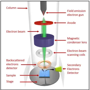
used in fabricating the optical components discussed in this thesis, such as electron-beam (e-beam)
lithography, dry and wet etching techniques such as inductively coupled plasma and reactive ion etching
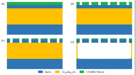
and micro-photoluminescence. In the following section the fabrication methods for hole-type photonic
crystals which involves a new e-beam resist with high temperature dry etching will be explained.
Chapter 4 will propose a new model for enhancing light emission from 2D materials and increasing
light-matter interaction through the use of rod-type photonic crystal cavities. Finite Difference Time
Domain simulation results of the cavity mode together with the enhancement obtained as the cavity
rods radius is changed is demonstrated. In addition, enhancements obtained as the 2D material is
allowed to dip inside the cavity is shown. Finally, a summary of the approach taken toward realising
the model experimentally with preliminary results will be discussed.
Chapter 5 will introduce a new scheme for realising photodetectors with site controlled III-V
semiconducting nanowires by epitaxial growth on Si. The introduction will briefly list the advantages
of nanowire based photodetectors over conventional planar photodiodes. The chapter will later present
results from fabricating the nanowire sites using state of the art e-beam lithography and CSAR as a
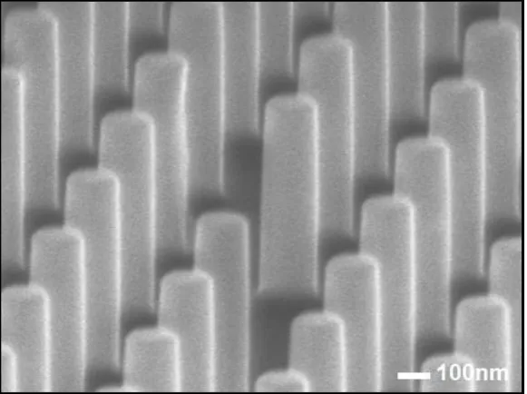
positive e-beam resist. Electron micrographs of the epitaxial growth results of InAs and GaAs
nanowires will be shown. The chapter will include investigation of the effect of growth temperature on
the successful formation of nanowires and their achieved lengths. Image analysis of electron
micrographs will be carried out and a discussion will follow to analyse the achieved nanowires lengths
for photodetection applications.
Chapter 6 will introduce current state of the art integrated QKD systems. An alternative approach that
harnesses quantum dot technology for single photon emission using GaAs as a host optoelectronic
material will be suggested. Comparisons will be made between the different approaches to realising
Chapter 1 – Introduction
1-10
preliminary experimental results will be presented before putting the proposal for the fully integrated
QKD chip.
Chapter 7 will summarise the results achieved in this thesis including the challenges and the limitations
faced throughout the research period. The chapter will discuss future plans that are currently being (or
will be) investigated to take the research of 2D material based rod-type photonic crystals single photon
Chapter 1 – Introduction
1-11
Bibliography
1 T. Polk, K. McKay, S. Chokhani. Guidelines for the selection, the configuration, and use of transport
layer security (TLS) implementations. NIST special publication 800-52 (2014)
2 P. W. Shor. Algorithms for quantum computations: discrete logarithms and factoring. Proc. 35nd
Annual Symposium on Foundations of Computer Science, IEEE Computer Society Press, 124-134 (1994)
3 D. Goodin. How the NSA can break trillions of encrypted web and VPN connections. ARS Technical
UK. https://arstechnica.co.uk/security/2015/10/how-the-nsa-can-break-trillions-of-encrypted-web-and-vpn-connections/ (accessed 10/10/2016)
4 P. W. Shor, J. Preskill. Simple proof of security of the BB84 quantum key distribution protocol. Phys.
Rev. Lett., 85, 441-444 (2000)
5 R. Renner, N. Gisin, B. Kraus. Information-theoretic security proof for quantum-key-distribution
protocols. Phys. Rev. A., 72, 012332 (2005)
6 C. H. Bennett, F. Bessette, G. Brassard, L. Salvail, J. Smolin. Experimental quantum cryptography. J.
Cryptology, 5, 3-28 (1992)
7 B. Korzh, C. C. W. Lim, R. Houlmann, N. Gisin, M. J. Li, D. Nolan, B. Sanguinetti, R. Thew, H.
Zbinden. Provable secure and practical quantum key distribution over 307 km of optical fibre. Nature Photon., 9, 163-168 (2015)
8 P. Jouguet, S. Kunz-Jacques, A. Leverrier, P. Grangier, E. Diamanti, Experimental demonstration of
long-distance continuous-variable quantum key distribution. Nature Photon., 7, 378-381 (2013)
9 Toshiba Cambridge Research laboratory. Toshiba QKD system.
http://www.toshiba.eu/eu/Cambridge-Research-Laboratory/Quantum-Information-Group/Quantum-Key-Distribution/Toshiba-QKD-system/ (last accessed 12/12/2016)
10 ID Quantique limited. An overview of QKD.
http://www.idquantique.com/quantum-safe-crypto/qkd-overview/ (last accessed 12/12/2016)
11 P. Kok, C. P. Williams, J. P. Dowling. Construction of a quantum repeater with linear optics. Phys.
Rev. A, 68, 022301 (2003)
12 K. Azuma, K. Tamaki, H. Lo. All-photonic quantum repeaters. Nature Commun. 6, 6787 (2015)
13 W. J. Munro, J. Azuma, K. Tamaki, K. Nemoto. Inside quantum repeaters. IEEE Journal of Selected
Topics in Quantum Electronics, 21, 6400813 (2015)
14 M. Sasaki, M. Fujiwara, H. Ishizuka, et al.. Field test of quantum key distribution in the Tokyo QKD
network. Optics Express, 19, 10387 (2011)
15 C. Elliott. Building the quantum network. New Journal of Physics, 4, 46.1-12 (2002)
16 E. Diamanti, H. Lo, B. Qi, Z. Yuan. Practical challenges in quantum key distribution. NPJ Quantum
Chapter 1 – Introduction
1-12
17 G. Brassard, N. Lutkenhaus, T. Mor, B. C. Sanders. Limitations on practical quantum cryptography.
Phys. Rev. Lett., 85, 1330-1333 (2000)
18 J. Zhang, M. A. Itzler, H. Zbinden, J. Pan. Advances in InGaAs/InP single-photon detector systems
Chapter 2 – Background and Theory
2-1
Chapter 2
Background and Theory
In this thesis, optoelectronic components for integrated quantum information devices are studied,
specifically for uses in quantum communications. The operation principles of these components utilise
the fundamental physical properties of semiconductors, quantum confinement and photonic crystals
(PhCs). This chapter will provide the necessary background materials and theory needed for
understanding these properties and how they are utilised to realise useful optoelectronic devices.
Semiconductors and Quantum Dots
2.1.1.
Basics
Semiconductor materials have their conductivity lie between that of insulators and conductors at room
temperatures. An attractive aspect of semiconductors is that the conductivity in these materials can be
engineered to suit different purposes1. Due to the periodicity of the crystal lattice structure of
semiconductor materials, an electron wave-function travelling through the lattice interacts with a
periodic electric potential. This periodicity results in discrete energies where the electron wave-function
is allowed to exist whilst providing other energies that the electrons are forbidden to have. The forbidden
and allowed energy ranges can be calculated by solving the Schrödinger equation for an electron
wave-function in the periodic lattice potential, where the solutions are known as Bloch waves2. These
solutions can be described visually as the electronic band structure for the lattice3. At both ends of the
Chapter 2 – Background and Theory
2-2
bands. For intrinsic semiconductors, the valence band is the highest range of electron energies that the
electrons can have at absolute zero temperature. On the other hand, the conduction band is the lowest
range of vacant electronic states. It will be shown later in this chapter that photonic band structures can
also be found for a photon wave-function travelling through a periodic structure of materials of different
dielectric constants.
Quantum dots (QDs) are formed in semiconductors by altering the system’s band structure such that
exciton confining potential wells are made4. This can be achieved by three dimensionally modifying
the physical structure of the system on a length scale smaller than the electron’s de Broglie wavelength.
If the confinement is large enough, an electrons’ and/or holes’ wave-function can be confined in all
dimensions. An electron in the QD material can be excited from the valence band to the conduction
band by absorbing a photon, leaving behind a hole, where the electron and the hole can bind together
due to attractive columbic forces forming an exciton. When the electron relaxes back to the valence
band, by combining with the hole, a single photon is emitted. This makes QD systems ideal for single
photon source applications such as quantum key distribution (QKD)5.
The energy of a photon emitted by a quantum dot is the sum of the bandgap energy of the quantum dot
material, the confinement energy and the exciton Coulomb energy, as shown in equation 2.1.
𝐸 = 𝐸𝑏𝑎𝑛𝑑𝑔𝑎𝑝+ 𝐸𝑐𝑜𝑛𝑓𝑖𝑛𝑒𝑚𝑒𝑛𝑡+ 𝐸𝐶𝑜𝑢𝑙𝑜𝑚𝑏 (2.1)
The confinement energy of an electron wave-function is directly dependent on the bandgap difference
between the host material and the QD material, and on the QD size. This can be calculated using the
particle in a box approximation. Coulombic attraction between the negatively charged electron and the
positively charged hole can influence the total photonic energy of the quantum dot. This attraction is
directly proportional to Rydberg’s energy and inversely proportional to the square of the dielectric
Chapter 2 – Background and Theory
2-3
Figure 2.1: Illustration of the self-organised growth of semiconductor QDs. A QD material is deposited on the substrate using
epitaxial methods. The lattice constant difference between the QD material and the substrate causes the QD layer to cluster
into QDs as its thickness is increased.
Conventionally, there are different forms of QD systems, for example, colloidal QDs6, Josephson
junction QDs7, however, the two forms that are of interest in this work are self-assembled QDs8 and
zero-dimensional defects in 2D materials9.
2.1.2.
Self-Assembled Quantum Dots
Self-assembled QDs are made by growing a thin semiconductor material very slowly, using Molecular
Beam Epitaxy (MBE) or Chemical Vapour Deposition (CVD), on top of another semiconductor
material of differing lattice constant10,11. After growing a few monolayers, the strain caused by the lattice
mismatch between the two semiconducting materials causes the uniform layer structure to collapse and
form three-dimensional islands as shown in Figure 2.1. This is known as the Stranski-Krastanov growth
technique12. The QDs are usually capped with a thick layer of the original material to enhance their
formation due to strain and protect them.
Different materials have been used to create self-assembled QDs such as GaSb/GaAs13, InAs/GaAs14,
InN/GaN QDs15.
2.1.3.
Defects in 2D Materials
2D materials are crystalline materials that are comprised of a single or a few layer atoms. Since the
discovery of graphene, 2D monolayer materials with unique optical properties, such as transition metal
Chapter 2 – Background and Theory
2-4
(MoS2) and tungsten diselenide (WSe2). These were found to exhibit similar optical properties to
semiconductor materials such as GaAs. Many TMDC monolayers, such as the ones previously
mentioned, have a direct bandgap and their optical emission wavelength lies in the visible range making
them good light absorbers/emitters. In addition, TMDC monolayers benefit from the unique optical
properties of quantum wells due to their two-dimensional nature giving excitons discrete energy states.
The simplest and most abundant type of QDs in semiconductor TMDCs are vacancies, while the less
commonly found type are dopants in the lattice16. The introduction of defects such as atomic vacancies
can be done by fluctuating the growth conditions of CVD grown TMDC monolayers. Dopants in the
lattice can be introduced through ion/electron irradiation, high temperature annealing and plasma
processing. Similar to QDs in bulk semiconductor materials such as GaAs, QDs in 2D materials have
been reported to be capable of emitting single photons9, making them a potential source of single
photons for quantum information applications.
Figure 2.2: (a) A schematic illustration of the atomic structure of a typical, (a) pure, (b) defective and (c) impure MoS2
monolayer flakes.
Photonic Crystals
2.2.1.
Photonic Band Structure
In the first part of this chapter, the basics of the electronic band structure in semiconductor crystal
materials was summarised. In this section, an overview of the photonic band structure in PhCs will be
introduced. Interestingly, the theory of the electronic wave-functions in a semiconductor crystal and
photonic wave-functions in PhC are very similar17. A PhC consist of a periodic optical structure of
different materials with different dielectric constants. PhCs can be found in nature in different places,
an example of this is the colourful pattern on an insect’s eye as shown in Figure 2.3.
(b)
Chapter 2 – Background and Theory
2-5
Figure 2.3: *An image of a female Tabanus horse fly showing the colourful pattern on the fly’s eye which results from the
diffraction of white light into different colours (a). An electron micrograph image of a fly’s eye showing the periodic pattern
that causes the colourful appearance of the eye (b). *Royalty free from: http://www.earthporm.com/11-incredible-eye-macros/
Figure 2.4: Illustrations of a 1D (a) and a 3D (b) PhC. The blocks with different colours, yellow, grey and cyan represent
materials with supposedly different dielectric constants.
Figure 2.5: Examples of 2D PhCs showing (a) a hexagonal array hole-type and (b) a square array rod-type lattice. The grey
materials is usually made of different dielectric constants in comparison to the surrounding material. Both of those types will
be explored and used for making photonic devices in this thesis, see chapters 4 and 6.
The periodicity in the photonic structure can be in one, two or three spatial dimensions, Figure 2.4
shows examples of a one and three-dimensional PhC, whilst Figure 2.5 shows examples of
Chapter 2 – Background and Theory
2-6
The different properties of PhCs including the periodic lattice constant of the lattice, the shape and size
of the periodic materials and the different dielectric constants of the materials allows the propagation
of light with certain wavelengths and prohibits the propagation of other wavelengths. The range of
wavelengths that are prohibited from propagating through the lattice is known as the photonic bandgap
and is caused by the destructive interference of the light’s wave-function due to reflection at the
alternating layers. This is analogous to the concept of an electronic bandgap that prohibits the
propagation of electronic wave-functions with certain energies. To illustrate this idea, Figure 2.6 shows
the transmission spectrum obtained as a light wave travels through a square PhC structure made of high
dielectric rods in air, and is collected by a flux region at the opposite side of the source18.
Figure 2.6: An example of a simulation setup of a wave emitted from a plane wave source and propagating through a PhC
towards a detector on the other side. (b) The transmission spectrum obtained from the detector showing a wide bandgap range
from 0.250 to 0.425 with photonic edge states on both sides of the band gap.
The Poynting vector is the rate of energy transfer per unit area of an electromagnetic field19. In the
Finite Difference Time Domain (FDTD) simulation in Figure 2.6, the power spectrum transferred
through a flux region for a field frequency ω is calculated via the integral of the Poynting vector over
the flux region, and subsequently accumulated over n-time steps. The process is repeated for every
frequency to construct the flux spectrum.
2.2.2.
Photonic Crystal Resonators and Waveguides
If a defect in the PhC lattice is introduced, a photonic cavity can be created in the structure. Normally,
Chapter 2 – Background and Theory
2-7
creating defects is by changing the size and/or the dielectric constant of one or more of the lattice cells.
In the example shown in Figure 2.7 (a), removing one of the rods creates a monopole defect cavity.
Introducing a defect can cause a localised state to form within the bandgap of the dispersion spectrum
of the crystal. This means when a light wave travels through the lattice, somewhere within the bandgap
transmission curve, a state can be found corresponding to the cavity mode, as illustrated in Figure 2.7
(b).
In the one-dimensional Bragg mirror approximation, a photonic cavity in a material with refractive
index, n (𝑛 = 1 in the illustration of Figure 2.7), has a mode when the cavity length 𝐿𝑐𝑎𝑣 is equal to an
integer multiple, 𝑚, of the intra-cavity half wavelength, λ, and is given by:
𝐿𝑐𝑎𝑣=𝑚𝜆2𝑛 (2.2)
The resonance occurs when there is a constructive interference caused by reflections of the wave due
to the photonic bandgap. This constructive interference produces a sharp cavity mode within the
bandgap region.
Figure 2.7: An example of a simulation setup of a wave emitted from a plane wave source and propagating through a PhC
structure towards a detector with a removed hole forming a cavity. (b) The transmission spectrum obtained from the detector
showing an opened cavity mode state within the band gap. The inset shows the Ey field profile of such a cavity.
The defect within a 2D PhC can be designed to confine a desired cavity mode wavelength within the
Chapter 2 – Background and Theory
2-8
internal reflection rather than Bragg reflection. Krauss et al. were the first people to show
experimentally a 2D PhC cavity mode that harnesses total internal reflection for light confinement20.
The confinement strength of any cavity is determined primarily by the factor of the cavity. The
Q-factor of a cavity is defined mainly by two parameters related to the cavity mode, these are the mode’s
frequency (or wavelength), 𝜔, and the lifetime of a photon confined inside the cavity, 𝜏. The lifetime
of a photon inside the cavity can be rationally thought of as the duration a photon can stay within the
cavity before it is scattered or absorbed. Ideal cavities have an infinite lifetime, i.e. the photons can be
trapped inside them without escaping. In practice however, the lifetime of a cavity is finite. The inverse
of the lifetime is the cavity decay rate, 𝜅:
𝜅 =𝜏1
𝑐𝑎𝑣 (2.3)
The Q-factor can then be defined as:
𝑄 =𝜔𝜅 (2.4)
The most common PhC cavity design comprises one or more air-holes removed from a PhC hole lattice
fabricated on a high dielectric constant material such as GaAs or Si. The most common of these are the
H1 and the L3 cavities that are made of one and three removed holes, respectively. Scanning Electron
Microscopy (SEM) images of the H1 and L3 PhCs are shown inFigure 2.8. Another common cavity
design is based on the removal of one rod of a high dielectric constant periodic rod structure surrounded
by air. SEM images of such a structure is shown in Figure 2.9. The latter cavity design will be the main
type used in chapter 4, whilst the former will be mainly used in chapter 6.
The PhC cavities discussed before are defects within the photonic lattice and can be considered as a
localised disruption to the periodicity that act as optical resonators capable of confining electromagnetic
modes of discrete wavelengths located within the photonic bandgap wavelength range. A PhC
waveguide can be considered as a series of specially coupled point defects. Coupling between these
Chapter 2 – Background and Theory
[image:28.595.153.444.299.516.2]2-9
Figure 2.8: (a) An example of an H1 hole-type PhC cavity. (b) An example of an L3 hole-type PhC cavity. The two figures
show one and three removed holes of the lattice forming H1 and L3 cavities, respectively.
Figure 2.9: An example of a hexagonal lattice H1 rod-type PhC cavity, showing one missing rod from the hexagonal rods
lattice to form a rod-type photonic cavity.
is confined in all directions but is allowed to travel along the series of defects. In a similar fashion to
PhC cavities, PhC waveguides can utilise total internal reflection to confine light in the third dimension
whilst being confined due to the photonic bandgap in the other two dimensions.
A single mode waveguide can be created by removing a row of holes in a hole-type PhC, such that there
exists only one guided mode wavelength within the bandgap of the lattice. This makes PhC waveguides
Chapter 2 – Background and Theory
2-10
due to its selectivity to couple to a discrete set of wavelengths21. A row of missing holes is called a W1
type waveguide and will be the main type considered in this thesis, see Figure 2.10.
Figure 2.10: SEM image of a typical W1 PhC waveguide designed for coupling to GaSb QDs with emission wavelengths of
~1250 nm. The waveguide is formed by creating a line defect in the lattice by simply omitting a line of holes to create a
propagating mode in the photonic bandgap system.
W1 waveguides are important since they can cause slow light effects22. Slow light is a term used to
describe light travelling through a medium with a group velocity that is much lower than the speed of
light in that medium. Slow light has many important applications in quantum information. This is
because by slowing light as it travels through a medium, stronger light-matter interactions can take
place, providing many opportunities for applications in optical buffering and quantum memories23,24. In
chapter 6, slow light is suggested to be used in phase modulators, hence shortening the needed
waveguide length for creating π-phase modulation compared to conventional phase modulators.
2.2.3.
Purcell Enhancement
The advantage in using a photonic cavity system to couple to a single photon emitter such as a QD is to
increase the spontaneous emission rate of single photons from the QD25. This rate of single photon
emission is directly related to the bit rate achievable when the system is used in a QKD chip. By placing
a QD inside a photonic cavity, the electric field of the cavity mode can interact with the QD’s ground
and excited state. Chapter 3 will show how a cavity is fabricated around a QD for this type of experiment
Chapter 2 – Background and Theory
2-11
The enhancement in the spontaneous emission rate of an emitter such as a QD coupled to a cavity
resonator is known as Purcell enhancement26. When an emitter decays in a cavity, the cavity confines
the photon spatially in a small region and enhances the electric field locally. The Purcell factor is
maximised when the QD that is in resonance with the cavity mode and its dipole is aligned with the
maximum of the cavity mode’s electric field. When this is the case, the Purcell factor can be written as
follows:
𝐹 =4𝜋32𝑄𝑉(𝑛𝜆)3 (2.4)
where V is the mode volume. This means that the Purcell effect is directly related to the Q-factor of the
cavity. Increasing the Q-factor whilst keeping other parameters constant transfers the cavity-QD
coupling from the weak coupling regime to the strong coupling regime where the cavity and the QD
have similar life times27. However, strong coupling is not required for the case of a QD coupled to a
micro-cavity for single photon source applications. The mode volume, on the other hand, is related to
the cavity mode’s wavelength divided by the refractive index of the cavity. Small mode volumes
enhance the interaction strength between the cavity mode’s electromagnetic field and the quantum
emitter. For example, H1 and L3 cavities have been shown to have mode volumes in the order of (𝑛𝜆) 3
,
where n is the refractive index of the semiconductor material in which the mode is confined in, making
them useful for single photon emission applications17. There are a number of tools that can be used to
find these parameters. An example of one of these tools that was mainly used in this thesis is discussed
Chapter 2 – Background and Theory
2-12
Single Photon Detectors
Single photon detectors (SPDs) are one of the main components that determine the speed and efficiency
of a QKD system28. An ideal SPD is expected to click every time it receives a photon, at an arbitrary
speed29,30. Practical SPDs that are incorporated in QKD systems are far from ideal. For example, the
quantum efficiency, which is the percentage of photons incident on the device’s photoreactive surface
and produce charge carriers, may be less than 100%. The dark count, which is the rate the detector
outputs pulses in the absence of any incident photon, and the dead time, which is the time in which a
detector is not capable of detecting a photon after a photon detection event, are both usually non-zero
in practice. The dead time also reduces the “photon number resolution”, which is the ability to
distinguish the number of photons in an incident pulse. The time jitter is also an important factor, it can
be defined as the time delay variations between the input of the optical signal and the output of the
electrical signal. This in practice may also be non-zero.
There are different physical methods that allow the realisation of SPD devices. The first uses
superconducting nanowires that are typically 5 nm thin, 100 nm in width and a few hundreds of microns
in length patterned in a grid like structure31-33. During operation, the wire is cooled below its
superconducting critical temperature and a DC bias current that is close to but less than its
superconducting critical current is applied. When a photon is absorbed by the nanowire grid, it breaks
electron Cooper pairs and reduces the local critical current below that of the bias current, causing an
increase in resistance at the region of the incident photon. This perturbation in resistance causes a
change in the bias current, typically measurable by sensitive electronic instruments. Superconducting
nanowire SPDs are known to have high quantum efficiency and relatively small dark counts, in
comparison to avalanche photodetectors (APDs) that will be described later. However, the limiting
factor that prevents this technology from being incorporated in commercial products in the future, is
their operation temperature which is typically required to be only a few degrees above absolute zero.
A more interesting technique in realising SPDs is by exploiting the avalanche effect when a P-I-N
Chapter 2 – Background and Theory
2-13
In the next section, a brief overview of P-I-N junctions together with the working principles of APDs
will be given as background material for chapter 5 which involves using nanowire P-I-N junctions for
photodetection.
2.3.1.
P-I-N Junctions
In section 2.1.1, the basics of semiconductor materials were introduced. It was introduced that
semiconductors have been widely used in electronic devices due to the ability to engineer their
conductivity for different applications. Changing the conductivity can be done by doping the
semiconductors with atoms to introduce negative (n-doping) and positive (p-doping) charge carriers,
electrons and holes. In the n- and p-doped regions, the carrier concentrations are a few orders of
magnitude higher than the concentration of carriers in the intrinsic region. Sandwiching an intrinsic
semiconductor region between an n-doped and a p-doped region makes a p-i-n junction. This structure
has many applications in high power electronics and is suitable for fast switches, attenuators and
photodetectors. The latter is the main use for p-i-n junctions in this thesis. Between the p-i-n junction,
there exists a layer even larger than the intrinsic region, known as the depletion region. This is formed
by charge carriers combining and annihilating one another through diffusion from the p- and the
n-doped regions. This diffusion becomes limited by the electric field created by positive and negative ions
left behind in the n and p regions, respectively.
Under forward bias, the p-type region is connected to the positive terminal of a power source and the
n-type is connected to the negative terminal. Electrons and holes from the n-type and the p-type regions
are forced towards the intrinsic region due to the potential difference of the source. Some charge carriers
recombine at the intrinsic region and others continue to flow through the opposite side of the junction
creating an electric current.
When a p-i-n junction is reverse biased, the depletion region widens and ordinarily the junction does
not conduct, except for a small leakage current. If a photon of sufficient energy is absorbed by the
Chapter 2 – Background and Theory
2-14
region, as shown in Figure 2.11. The applied reverse bias field pulls the electrons and holes, out of the
region, toward the source’s terminal, causing a current flow34.
Figure 2.11: (Left) p-i-n junction under reverse bias, showing the regions of majority electron and hole carriers, an incident
photon on the intrinsic region and the created electron-hole pair. (Right) Band diagram for the corresponding p-i-n junction
with the created electron-hole pair due to an incident photon on the intrinsic region. The excited electron and hole carriers are
attracted toward the n and p-regions respectively due to reverse bias, causing a current spike which can be amplified and
measured by sensitive electronics.
2.3.2.
Avalanche Multiplication
Avalanche multiplication is a phenomenon that can occur in semiconductor and insulating materials
where an electric current multiplication allows high currents to be generated in an otherwise insulating
materials27. In p-i-n junctions, the phenomena occurs when, following the absorption of a photon,
carriers are accelerated from the depletion region by the electric field of an applied reverse bias. If the
charge carriers have enough kinetic energy, collisions with other bound electrons can excite them across
the bandgap and create other free electron-hole pairs (secondary carriers). These secondary carriers
accelerate due to the applied bias and gain enough energy to create even more carriers in a cascaded
process. Hence a single photon can create a sudden increase in current at the junction. The current
created by the multiplicative process of carriers due to the absorption of a single photon makes
Chapter 2 – Background and Theory
2-15
Differential Phase QKD Protocols
The QKD scheme described in chapter 1, encodes quantum information on photon polarisations using
two non-orthogonal bases. An alternative encoding approach uses the phase difference between
successive photon pulses interfering at a beam splitter at the end of a Mach-Zehnder interferometer.
This method of encoding information is known as Differential Phase Shift (DPS) QKD35.
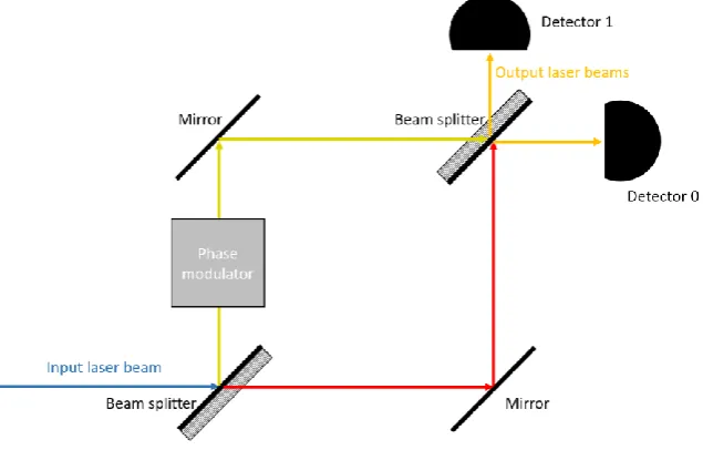
One of the key components in a DPS-QKD systems is a Mach-Zehnder interferometer. To illustrate the
operation principles of DPS-QKD, it is important to explain how a Mach-Zehnder interferometer work
for large photon number pulses. In this type of interferometers, the input laser beam is split in a 50:50
beam splitter, resulting in two beams, one can be called the modulated beam (marked yellow) and the
[image:34.595.141.459.360.563.2]other can be called the reference beam (marked red), as shown in Figure 2.12.
Figure 2.12: A block diagram of a typical DPS-QKD system with two pulses, coloured red and yellow, taking the different
path in the Mach-Zehnder interferometers. The laser is input from the bottom left as shown by the blue arrow and split by a
beam splitter. One arm contains a phase modulator which causes phase shifting one arm relative to the other. Constructive and
destructive phase shifting can be recorded by detectors 0 and 1 respectively.
Let’s define 𝑙1 and 𝑙2 as the total path length for the modulated and reference beams respectively. When
the light passes through a glass beam splitter it exhibits a phase shift equivalent to 2𝜋𝑡/𝜆, where 𝑡 is
Chapter 2 – Background and Theory
2-16
first beam splitter, a 𝜋 phase shift from the top mirror, a 2𝜋𝑡/𝜆 from the last beam splitter, and the path
length of 2𝜋𝑙1/𝜆, before reaching detector 0 . This gives a total of
2𝜋 + 2𝜋 (𝑙1+ 𝑡
𝜆 )
The reference beam takes a phase shift of 2𝜋𝑡/𝜆 as it goes through the first beam splitter, a 𝜋 phase
shift as it gets reflected by the bottom mirror and another 𝜋 phase shift as it gets reflected by the second
beam splitter toward detector 0. Hence the phase difference between the two beams 𝜙, which is caused
by the phase modulator is:
2𝜋 + 2𝜋 (𝑙1+ 𝑡
𝜆 ) − 2𝜋 − 2𝜋 (
𝑙2+ 𝑡
𝜆 ) = 𝜙
2𝜋 (𝑙1− 𝑙2
𝜆 ) = 𝜙
In a similar fashion, the phase difference between the two arms for detector 1 is:
2𝜋 + 2𝜋 (𝑙1+ 2𝑡
𝜆 ) − 𝜋 − 2𝜋 (
𝑙2+ 2𝑡
𝜆 ) = 𝜙
𝜋 + 2𝜋 (𝑙1− 𝑙2
𝜆 ) = 𝜋 + 𝜙
Hence, it is clear to note that when the phase modulator causes a zero phase shift, there is a constructive
interference on the path to detector 0, and a destructive interference to detector 1. By varying 𝜙, this
condition can be changed, hence changing the probability of arrival at either detector.
A simplified example of a DPS-QKD system is shown inFigure 2., where Alice generates a train of
single photon pulses and passes it through a Mach-Zehnder interferometer. In the interferometer, Alice
splits the signal through a beam splitter, and applies a random phase modulation of 0, π2, 3π2, or π on one
arm and recombines the two arms at the junction of a second beam splitter. She later sends the signal to
Bob through a quantum channel such as a fibre optic or free space. At Bob’s side, he performs a similar
Chapter 2 – Background and Theory
2-17
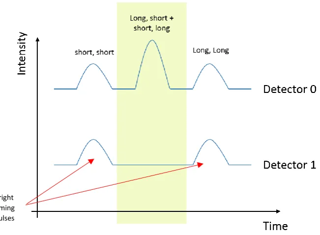
or π2 phase-shift through one arm and recombines the two arms in a beam splitter. There are three
detection time slots at which Bob can measure. The first is when two consecutive pulses take the long
paths on Alice’s and Bob’s interferometers. The second is when the two pulses both take the short paths
of the interferometers. Both of these events aren’t of use in this protocol. The only used events are when
a pulse takes the long and short arm of Alice and Bob sides while the other takes the short and long
arms of Alice and Bob respectively, as shown in Figure 2.. If the interferometers on both sides are
matched, as when Alice and Bob use a similar basis, a 0 or π phase shift takes place between two
successive photon pulses, causing trigger events in either detector 0 or 1, as shown in Figure 2.. In a
real implementation, each single photon pulse is accompanied by one proceeding bright pulse for timing
purposes. The bright photon pulse will appear as two pulses on Bob’s detectors as it goes through the
two long and two short paths in Alice and Bob sides.
Figure 2.13: A block diagram of a typical DPS-QKD system with two pulses, coloured red and yellow, taking the different
path in the Mach-Zehnder interferometers.
After receiving the qubits, Bob announces publicly the time slots at which a photon was detected by
one of his detectors, but does not reveal which detector detected it. From Alice’s modulation data, she
can know which detector in Bob’s end recorded the event. By designating detection events recorded by
detector 0 and 1 as key bit values 0 and 1, respectively, they can share an identical bit string.
In an ideal system where there are no errors in the detection events, the sifted key created is
unconditionally secure. However, in practice, as discussed in chapter 1, all QKD systems have a
baseline error rate, hence error correction and privacy amplification procedures are essential in a
Chapter 2 – Background and Theory
[image:37.595.129.455.70.309.2]2-18
Figure 2.14: An example of a click event observed on detector 0 due to a 0 degrees phase shift representing a 0 bit. This occurs
when two consecutive pulses take opposite and alternate arms on Alice and Bob’s ends. The figure also shows timing pulses
measured by the detector.
After error correction, when the error threshold is low enough to allow carrying on with the protocol,
to nullify any information that may have been obtained by an eavesdropper, Eve, privacy amplification
is performed36. This allows making Eve’s information of the final shared key extremely small. In
privacy amplification, Alice and Bob apply hash algorithms that uses the error free shared key as an
input and outputs a new shorter key.