roughness effects in AlGaN/GaN intersubband devices
GRIER, Andrew, VALAVANIS, Alex, EDMUNDS, Colin, SHAO, J, COOPER, J.
D., GARDNER, G, MANFRA, M. J., MALIS, Oana, INDJIN, Dragan, IKONIC,
Zoran and HARRISON, Paul <http://orcid.org/0000-0001-6117-0896>
Available from Sheffield Hallam University Research Archive (SHURA) at:
http://shura.shu.ac.uk/11085/
This document is the author deposited version. You are advised to consult the
publisher's version if you wish to cite from it.
Published version
GRIER, Andrew, VALAVANIS, Alex, EDMUNDS, Colin, SHAO, J, COOPER, J. D.,
GARDNER, G, MANFRA, M. J., MALIS, Oana, INDJIN, Dragan, IKONIC, Zoran and
HARRISON, Paul (2015). Coherent vertical electron transport and interface
roughness effects in AlGaN/GaN intersubband devices. Journal of Applied Physics,
118 (224308), 224308-1-224308-9.
Copyright and re-use policy
See
http://shura.shu.ac.uk/information.html
Sheffield Hallam University Research Archive
Coherent vertical electron transport and interface roughness effects in
AlGaN/GaN intersubband devices
A. Grier,1 ,a)A. Valavanis,1
C. Edmunds,2
J. Shao,2
J. D. Cooper,1
G. Gardner,3, 4
M. J. Manfra,2, 3, 4, 5
O. Malis,2
D. Indjin,1
Z. Ikoni´c,1
and P. Harrison6
1)Institute of Microwaves and Photonics, School of Electronic and Electrical Engineering, University of Leeds, Leeds,
LS2 9JT, United Kingdom
2)Department of Physics, Purdue University, West Lafayette, Indiana 47907,
USA
3)Birck Nanotechnology Center, West Lafayette, Indiana 47907, USA
4)School of Materials Engineering, Purdue University, West Lafayette, Indiana 47907,
USA
5)School of Electrical and Computer Engineering, Purdue University, West Lafayette, Indiana 47907,
USA
6)Materials and Engineering Research Institute, Sheffield Hallam University, Sheffield S1 1WB,
United Kingdom
(Dated: 17 September 2015)
We investigate electron transport in epitaxially-grown nitride-based resonant tunneling diodes (RTDs) and superlattice sequential tunneling devices. A density-matrix model is developed, and shown to reproduce the experimentally measured features of the current–voltage curves, with its dephasing terms calculated from semi-classical scattering rates. Lifetime broadening effects are shown to have a significant influence in the experimental data. Additionally, it is shown that the interface roughness geometry has a large effect on current magnitude, peak-to-valley ratios and misalignment features; in some cases eliminating negative differential resistance entirely in RTDs. Sequential tunneling device characteristics are dominated by a parasitic current that is most likely to be caused by dislocations, however excellent agreement between the simulated and experimentally measured tunneling current magnitude and alignment bias is demonstrated. This analysis of the effects of scattering lifetimes, contact doping and growth quality on electron transport highlights critical optimization parameters for the development of III–nitride unipolar electronic and optoelectronic devices.
I. INTRODUCTION
Intersubband optoelectronic devices such as quan-tum cascade lasers (QCLs) and quanquan-tum-well infrared photodetectors (QWIPs) have predominantly been fab-ricated using lattice-matched AlGaAs/GaAs or In-GaAs/InAlAs heterostructures. Although a wide range of high-quality devices have been realized, these conven-tional materials present a number of intrinsic limitations. For example, terahertz-frequency (THz) QCLs1 are the most powerful electrically-driven compact sources of co-herent radiation in the 1–5 THz band, with numerous potential sensing and imaging applications in astronomy, pharmaceutical and security scenarios.2Peak THz emis-sion powers in excess of 1 W3 are now available. How-ever, the commercial impact of THz QCLs has been limited by the requirement for cryogenic cooling (cur-rently <200 K4). Emission frequencies are also limited to < 5 THz,5 principally by Reststrahlen absorption ef-fects, owing to the relatively small 36 meV longitudinal-optic (LO) phonon energy in GaAs, and this limits the range of potential spectroscopy applications of existing THz QCLs.
The AlGaN/GaN material system has been proposed as a highly-promising alternative to conventional III–
a)Electronic mail: [email protected]
absorption at both near-infrared30–32 and THz33 wave-lengths as well as mid-IR34 and THz35 electrolumines-cence have also been demonstrated, indicating that high-quality opto-electronic devices may soon be realized.
Sequential tunnelling devices rely on repeated tun-nelling and scattering of carriers through up to several hundred periods of a structure. It was first demonstrated in nitride devices by Sudradjatet al.36with 20–30 three-well periods of an Al0.15Ga0.85N/GaN structure at low
temperature with good agreement between the experi-mental and predicted subband-alignment voltages. Fol-lowing this, a thinner structure with 10 periods of a single well and AlN barriers was grown and compared with an-alytical expressions25 for current, however it was found that domain formation dominates the I–V characteris-tics, preventing investigation into the roles of scattering on transport. To date, there has been no detailed the-oretical study and comparison of devices which require scattering and tunnelling between several states per pe-riod, however several exist for HEMT structures.37,38
Several approaches exist for the modeling of RTD current–voltage characteristics including the transfer matrix,10 Wigner functions39–41 and non-equilibrium Green’s function (NEGF) methods.11 To date, nitride RTDs have been studied with the transfer matrix ap-proach42which assumes purely ballistic (coherent) trans-port through the double barrier structure, and also by the NEGF approach43 which is computationally inten-sive but describes scattering in the presence of coherent transport. Even fewer theoretical results are available for sequential tunneling transport due to its recent experi-mental realization.
In this work, we aim to unify transport modeling for RTDs and sequential tunneling devices by developing a modified form of the density matrix (DM) approach that uses relaxation terms calculated from all relevant scatter-ing mechanisms. The DM approach has been well studied and shown to have good I–V and output power agree-ment with experiagree-mental AlGaAs/GaAs QCLs.44By com-paring output from the model with high quality nitride experimental devices, we show the relative importance of coherent and incoherent transport mechanisms and the effect they have on critical characteristics such as the cur-rent peak-to-valley ratio, magnitude of curcur-rent and high temperature behavior.
II. RESONANT TUNNELLING DIODES
A. Device fabrication and characterization
Electrons in an RTD travel from a highly-doped emit-ter region into a double barrier structure with resonant quantized subbands and then on to a collector region. By applying a bias to the device, the quantized states move in and out of alignment with a distribution of car-riers in the emitter, causing NDR features in theirI–V
characteristics.
70 80 90 100 110 120 130 140 150 160 Position (nm)
-200 -100 0 100 200 300
Energy (meV)
E W
[image:3.595.322.539.74.225.2]C
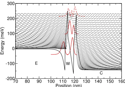
FIG. 1. Bandstructure and wavefunction plot of the Al0.18Ga0.82N 49 ˚A RTD at 0.136 V. The localized
wavefunc-tions are obtained using a ‘tight-binding’ scheme with the de-vice split into emitter (E), well (W) and collector (C) regions. The tight-binding Hamiltonian for the well section of the de-vice is achieved by replacing the extended bandstructure in the emitter/contact with a potential equivalent to the maxi-mum potential value of the barriers. The quantized emitter state and well confined states are shown in red.
Al0.18Ga0.82N/GaN RTDs with 49 ˚A wells (barriers
24 ˚A) were grown using plasma-assisted molecular beam epitaxy (MBE) on high-quality free-standing n++ GaN substrates, which were grown using hydride vapor phase epitaxy (HVPE) (dislocation density <5×106cm−2) and supplied by Kyma Technologies.19,20 Low Al com-position was used to suppress relaxation effects of the strained AlGaN barrier layers during growth/processing and also to minimize electrical breakdown through inter-action of the applied bias with polarization discontinu-ities. The emitter and collector regions consisted of GaN with silicon doping at a level of 1×1019cm−3 separated by 20 ˚A spacer layers from the well structure. After pro-cessing into 4×4µm mesas, the chips were then mounted on copper blocks and wirebonded to gold contact pads before measurement in a liquid nitrogen-flow cryostat.
B. Density-matrix model
In our DM model, the device is split into three sec-tions (the emitter, well, and collector) and it is assumed that the barriers are sufficiently thick or tall enough to limit transport to quantum tunneling only. This is ap-propriate since incoherent scattering will dominate trans-port within each section independently. We use the self-consistent Schr¨odinger–Poisson solver nextnano345
3
this system we solve the Liouville equation:
∂ρ ∂t =−
i ¯
h[H, ρ]− ρ
τ (1)
which describes the evolution of the density terms in time. Localized wavefunctions are obtained in each of the three sections of the device, using an effective mass Schr¨odinger solver46 that accounts for non-parabolicity effects. These wavefunctions represent a ‘tight-binding’ scheme where other sections of the device are replaced with barrier material. The resulting electron probability densities are shown in Fig. 1. These are then used as ba-sis states for coherent transport through the device. The density matrix is expressed in block form as:
ρ=
ρEE ρEW ρEC
ρWE ρWW ρWC
ρCE ρCW ρCC
(2)
where E, W and C refer to emitter, well and collector states respectively. Combinations of these labels such as EW, etc. (when not used as subscripts) simply refer to any interaction involving states in the two specified periods and are used to describe the coupling strengths and dephasing times in addition to the coherence terms here. Each of the element-blocks within Eq. (2) are sub-matrices, which represent the coherences of all pairs of states either within a given region (e.g.,ρEE) or between two different regions (e.g.,ρEW). In each of these blocks the density terms are unknown values to be calculated and refer to the ensemble average of the weightings for the basis states ρij = hcic∗ji. The physical
interpreta-tion of the diagonal (i =j) elements is the probability of an electron being found in state i, and therefore the
ith subband populations can be determined by knowing the total carrier density. The off-diagonal elements rep-resent the degree of polarization between statesiandj, which is interpreted as the coherence between the states.
ρECand its Hermitian adjoint are set to zero to indicate non-interaction between these sections. The emitter and collector reservoirs are set large enough to approximate a continuum of states such as those shown in Fig. 1. The size of the system is therefore (NE+NW+NC)2whereN is the number of states for each section. The Hamiltonian for the unperturbed system is:
H =
HEE HEW 0
HWE HWW HWC 0 HCW HCC
(3)
where the diagonal elements consist of the basis state en-ergies. The off-diagonal elements within the intra-region blocks (EE, WW and CC) are zero since no optical in-teraction is assumed. The inter-region blocks (EW, WE, WC and CW) describe the coupling between states and consist of the coupling strength (Rabi oscillation) terms calculated as47:
¯
hΩij ≈
q
hi|Hext−Hleft|ji ×
q
hi|Hext−Hright|ji (4)
where Hext and Hleft,right refer to the Hamiltonians (po-tentials) of the extended structure and of the ‘tight-binding’ sections, respectively. Several approaches are possible for the approximation of a tight-binding ap-proach for resonant tunnelling diodes; these are not as intuitive as the case for QCL or sequential tunnelling structures as the majority of the contact regions are flat with most potential drop occurring over the well struc-ture. Figure 1 shows how sections other than that being considered (emitter, well or collector) are replaced with a potential corresponding to the maximum value of the potential in the device. These are replaced so that the internal electric fields are still accounted for e.g. the po-tential substitution for the emitter region is performed after the first barrier.
If two energy levels of neighboring sections couple co-herently, electron wave packets can propagate (tunnel) through the barrier from one energy level to another. The coherent transport depends on the strength of the coupling, the detuning from resonance, and the lifetime of the coherence.
Electron wave packets within each section of the device lose phase coherence due mainly to intrasubband elastic scattering, and several methods have been proposed for the approximation of dephasing times. We use an ap-proach similar to that in Refs. 48 and 49 with the contri-butions from inter- and intrasubband scattering rates for the emitter and collector reservoirs. These calculations are performed for scattering due to LO phonons, acous-tic phonons, interface roughness and ionized impurities. Dephasing due to intrasubband events in the well region are neglected as these are highly dependent on the well state populations which is not known in advance. By in-cluding intersubband scattering here, carriers can tunnel from the emitter to the excited state of the well, and pro-ceed to scatter and tunnel to the collector from the well ground state.
The intrasubband electron–electron scattering rate was calculated to be approximately Wii = 1×10¹³s−1 at
77 K and this was applied to all subbands to account for dephasing by this mechanism. Formally, the relaxation terms should obey the Lindblad master equation to en-sure that the density matrix is positive definite. QCL simulations with a DM approach described here have re-ported negative populations at some in-plane wave vec-tors k.50 However, Fermi–Dirac averaged results retain positive populations and this was also observed in this work. To determine lifetimes, the total sheet-density of electrons (equal to the density of ionized impurities) was assumed to be distributed thermally across the contin-uum of states, with each subband electron temperature (Te) equal to the lattice temperature (Tlatt). The average
scattering lifetimesτij were then obtained by averaging
over the in–plane wave vector of the initial state to in-clude final state blocking as:
1
τij =
R
Wif(ki)fFD
i (ki)[1−ffFD(kf)]ki dki
where i and f refer to the initial and final wavevector states for the scattering transition, fFD
i is the Fermi–
Dirac distribution for the ith state, N is the 2D sheet density, E is the total energy of the initial state and ¯hω
is the transition energy (accounting for phonon interac-tions where applicable). Averaging in this way avoids the unbounded number of density matrices possible for the in–plane wavevector. Dephasing rates are then cal-culated from these states as48,49:
1
τ||i,j
= 1 2τi +
1 2τj +
1
τii +
1
τjj −
2
√τ
ifr,ii×τifr,jj (6)
where τi is the state lifetime calculated as 1/τi =
P
j1/τij and τii and τifr,ii are the total and interface
roughness intrasubband scattering lifetimes respectively. The scattering rates and dephasing times associated with all scattering rates except for interface roughness can be calculated a priori. However, interface roughness scat-tering rates exhibit a sample-specific dependence on the quality of epitaxial growth.
We use an interface-roughness (IFR) scattering model51 in which the roughness follows a Gaussian po-tential with r.m.s. height ∆ and correlation length Λ. The scattering of carriers between states with an initial wavevectorki is given by:
Wif(ki) =πmc
¯
h3 ∆
2Λ2β(k
i)
X
I
V0Ψ∗f(zI)Ψi(zI)
2 (7)
whereIis an index indicating each AlGaN/GaN interface and V0 is the step in conduction band potential at the interface and
β(ki) = e−(k 2
i+kα2)Λ2/4I
0
kikαΛ2
2
Θ(kα2)[1−Pf(kα)]
(8) whereI0(·) is the regular modified cylindrical Bessel func-tion of zeroth order, ki and kα are the initial and final
electron wavevectors respectively, andPf is the
occupa-tion factor of the final wavevector. Θ(·) is the Heaviside step function, which is used to ensure that transitions are energetically permissible. Eq. (7) indicates that the scattering rate (and therefore dephasing time) will de-pend on the parameters ∆ and Λ which are determined by the growth quality. The effect of varying these pa-rameters is discussed in the results section. These rates are then used in the relaxation matrix:
ρ τ =
−ρ11 τ1 +
N
P
i6=1
ρii
τi1 · · ·
ρ1N τ||,1N
..
. . .. ...
ρN1
τ||,N1 · · · − ρNN
τN +
N
P
i6=N
ρii
τiN (9)
which is the final term in Eq. (1). These relaxation ma-trix elements determine the duration of coherence be-tween states, and therefore the magnitude of current and
state broadening. For significant electron wave propa-gation between regions, the Rabi oscillation frequencies (coupling strength) must be faster than these dephasing terms.
C. Steady state solution and current
The Tsu–Esaki formalism for current assumes a Fermi– Dirac distribution of carriers in the reservoir regions with Fermi energies pinned to contacts on each side of the de-vice to determine the magnitude of current. However, since the subband quasi-Fermi energy was set before the calculation of scattering rates, the solution for the diago-nalρelements naturally resembles a Fermi–Dirac distri-bution in each reservoir. Eq. (1) is solved with ∂ρ∂t = 0 to find the steady-state emitter and well state populations and coherences using the Armadillo/LAPACK C++ lin-ear algebra libraries.52,53To make the system inhomoge-neous, trace conditions for the reservoirs were set so that
P
iρii = 1. Physical quantities such as current density
for this device can be extracted from the solved density matrix asj= Tr(ρJ), with
J =ei
¯
h[H,z] (10)
where e is unit charge and z consists of the dipole ma-trix element termszi,j = hΨi|z|Ψji. It is worth noting
that second-order density matrix approaches have shown better agreement with experimental QCLs54 due to the asymmetrical form of tunneling into wavevectors above the Γ point around resonance; this was neglected here for simplicity and to demonstrate the general approach. Nevertheless, we show in Section II D that our first-order model achieves good agreement with experimental re-sults.
D. Results
Experimental I–V characteristics at 77 K are shown in Fig. 2. The experimental device shows a resonant peak at 0.165 V with a plateau-like feature between 0.17–0.18 V. Previous experimental measurements of Al-GaAs RTDs have also observed plateau features in their
5
0.1 0.12 0.14 0.16 0.18 0.2 0.22 0.24 0.26
Voltage (V) 100
200 300 400 500 600 700 800
Current (
µ
A)
77 K 300 K
FIG. 2. Experimental I–V characteristics for the Al0.18Ga0.82N RTD with a 49 ˚A well and mesa size of 4×4µm
2
at 77 K. The positive polarity refers to positive bias applied to the top of the mesa and corresponds to electron injection from the left side in Fig. 1.
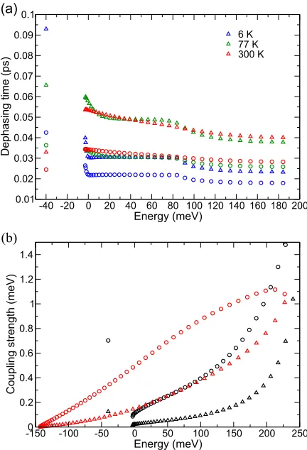
Fig. 3(a) shows the calculated dephasing times over a range of temperatures between states in the emitter reservoir and the ground and first excited states of the quantized well atV = 0.136 V where the simulations pre-dicted a peak current. The slight discrepancy with the experimentally measured 0.165 V resonance is attributed to contact resistance effects, as explained later in this section. Dephasing times were found to vary signifi-cantly with temperature, decreasing from 94 fs at 6 K to 33 fs at 300 K between the quantized emitter state (at
E = −40 meV) and the ground state in the well. This is due to a significant increase in intrasubband scatter-ing caused mainly by interface roughness and impurity scattering. Dephasing time decreases at higher energies in the emitter reservoir due to the absence of final-state blocking (as they are weakly populated) leading to a faster scattering rate. This absence of final-state block-ing causes the dephasblock-ing time for continuum states at 6 K to be lower than that at higher temperatures. Addition-ally, the smaller population of the first excited state in the well contributes to a reduction in the dephasing time for tunnelling in and out of this state. Initial coupling strengths given by Eq. (4) were found to yield currents larger than the experimentally measured values, and a scaling factor of 25% was used to account for this overesti-mation. This is a predictable error since the anti-crossing energy will be overestimated by the tight-binding Hamil-tonian. Extraction-coupling strengths were calculated to be larger than emitter-coupling strengths and therefore play a less significant role in determining the vertical elec-tron transport in these devices. Fig. 3(b) shows the calcu-lated coupling strengths for both EW and CW blocks of the Hamiltonian versus energy. These show that the cou-pling strength between the quantized emitter state and
FIG. 3. Calculated dephasing times (a) and coupling strengths (b) for the quantized emitter states for electrons tunnelling from the emitter states into the ground (triangles) and first excited state (circles) of the RTD well at 0.136 V. A low temperature approximation is used, such that electrons are assumed to initially occupy only states at the bottom of each quantised emitter subband.
well states is large due to its localization at the inter-face. Coupling strengths between the first excited state in the well and the continuum reservoir states is higher due to the reduced confinement of the triangular barrier potential at these higher energies.
[image:6.595.322.538.70.387.2] [image:6.595.65.276.76.225.2]0 50
100 150
200 250
300 350
400 0 0.5 1
1.5 2
2.5 3
3.5 4
0.5 1
1.5 2
2.5 3
PVR
Correlation length (Å)
[image:7.595.323.537.76.228.2]Roughness height (A °) PVR
FIG. 4. Peak to valley ratio versus correlation length (Λ) and roughness height (∆) interface roughness parameters used in dephasing calculation at 77 K.
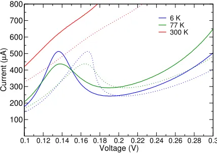
band elastic events are of greatest importance. These re-sult in a small change in electron wavevector, and there-fore the exponent term in Eq. (8) remains significant at large values of Λ. Fig. 5 shows the calculatedI–V curve from 0.10–0.30 V using interface-roughness parameters ∆=2.8 ˚A and Λ=100 ˚A. Excellent agreement is obtained with the experimentally measured location of the current peak as well as the magnitude of the PVR. These rough-ness parameters are typical for AlGaAs/GaAs structures such as QCLs61 suggesting that interface quality is very high in these MBE grown structures.
The broadening due to dephasing gives improved agreement for the PVR compared with the transfer ma-trix method which assumes purely ballistic transport.42 A dephasing time of 0.065 ps at 77 K for the ground-to-ground state tunnelling process results in a full-width at half-maximum (FWHM) broadening of around 10 meV and this increases to ∼16 meV for higher energy sub-bands. Increasing current due to alignment of the first excited state in the well is underestimated by the model (current at the 0.165 V peak is achieved again at 0.29 V in the simulation, rather than 0.25 V observed experimen-tally) and this is likely due to overestimating the relevant confinement of the excited state in the well compared to the ground state. Our model elucidates that the experi-mental current peak atV=0.165 V arises from the align-ment with the quantized emitter state rather than the continuum above the emitter band edge where a com-bination of lower population, dephasing time and cou-pling strength is insufficient to induce an NDR feature. A previous study19 of nitride RTDs has also observed alignment features prior to a significant NDR feature and we infer from our model that these can be attributed to alignment with the emitter band-edge in cases where the alignment energies are sufficiently separated. The depth and variance in spatial position of the quantized emit-ter state is highly sensitive to maemit-terial parameemit-ters which could vary significantly between structures such as
con-0.1 con-0.12 con-0.14 con-0.16 con-0.18 0.2 0.22 0.24 0.26 0.28 0.3 Voltage (V)
100 200 300 400 500 600 700 800
Current (
µ
A)
[image:7.595.57.275.76.211.2]6 K 77 K 300 K
FIG. 5. Simulated current with (dashed) and without (solid) an external series resistance applied to the data.
tact doping, spacer thickness and barrier alloy fraction. It is noteworthy that the position of the NDR is close to that calculated theoretically but lies 29 mV above it. This suggests the presence of a contact resistance, Rs, in series with the device that shifts the physical NDR to higher voltages. To estimate the magnitude of the series resistance, we find theRSas62:
Rs=
(V∗−V)
IA(V)
(11)
whereV is the simulated voltage drop across the RTD at resonance,V∗ is the resonant experimental voltage
(in-cluding contacts) and IA is the resonant current. The
resulting shifted calculatedI–V curves with a 60 Ω con-tact resistance are shown in Fig. 5; this value is simi-lar to those in Ref. 62. Alternatively, agreement can be achieved by assuming a constant voltage drop due to con-tacts. However, it is likely a combination of these effects is present.
7
E. Limitations of the model
The model presented in this section has been shown to faithfully replicate the disappearance of an NDR feature at high temperatures. Additionally, it allows the effect of changing interface roughness parameters to be calculated conveniently with semi-classical scattering rate calcula-tions. However the continuum of states used to approxi-mate the emitter and collector reservoirs places an upper limit on the dephasing times where output characteristics will appear physically correct. This is due to the require-ment for dephasing to be short enough to broaden the current contribution sufficiently when out of alignment and remove local spikes during instances of exact align-ment. The ‘continuum’ state separations are sensitive to the well width used to approximate them, and con-vergence checks performed indicate that lengths greater than 70 nm are sufficient. With contact lengths varied between 70 nm, 100 nm (the length used in these simula-tions) and 200 nm the change in current and PVR values are negligible.
The model does not account for dynamic changes in state populations that will affect the electric field. This is due to the use ofnextnano3 before the density matrix calculation and therefore we neglect the effect of pro-cesses such as dynamic well charge build up. However this is also the approach used in Refs.42 and20 and does not affect conclusions regarding the effect of tempera-ture and IFR parameters on the PVR. Finally, the cou-pling strength between the well and reservoirs required scaling indicating that this may not be a predictive ap-proach. This is attributed to the large flat potential lying far above the bandedge that will provide significant non-zero contributions in Eq. 4 immediately beyond where the extended bandstructure is replaced. This coupling strength calculation will also lead to unphysical results if weakly bound states with large overlaps between sections are included (such as with the second excited well state if present). This is expected this type of density matrix approach since it is assumed that all transport is due to tunnelling only and requires the ‘tight-binding’ condition to be fulfilled. Therefore the applicability of this model to devices with very thin layers may be limited however a full investigation into the RTD structures where this regime holds is beyond the scope of this article.
III. SEQUENTIAL TUNNELING DEVICES
In this section we compare the theoretical and ex-perimental characteristics of a periodic triple-well struc-ture similar to that in Ref. 24 with a period thick-ness of 178 nm in which interface and domain forma-tion effects are not expected to dominate. Ten periods of the structure were grown on a GaN substrate using MBE. The epitaxial layer thicknesses in each period are
23/47/10/23/26/49˚A where the Al0.15Ga0.85N barriers
are in bold, the GaN wells are in regular text, and the
100 120 140 160 180 200 220
Position (nm) -400
-300 -200 -100 0 100 200
Energy (meV)
Contact doping 2x1018 cm-3
Contact doping 4x1018 cm-3
0 5 10 15 20 25 30 35
-400 -200 0 200 400
Energy (meV) 1
2
3
4
(a)
(b)
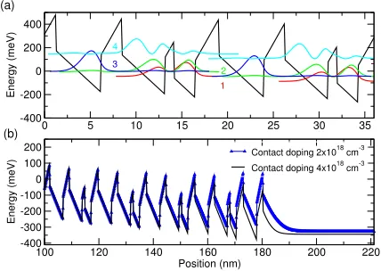
FIG. 6. (a) Bandstructure and wavefunction plot of the se-quential tunneling device under an 18.6 kV/cm bias assuming a linear voltage drop. (b) Trailing few periods of the structure and contact region calculated withnextnano3.
underlined well is n-doped with Si at 1×1017cm−3 to give a sheet density of 5×1010cm−2 per period. Con-tact layers were n++doped at 2×1018cm−3. The calcu-lated bandstructure of the device at 18.6 kV/cm is shown in Fig. 6(a), assuming a linear voltage drop across the device. The entire structure is also modeled with the
nextnano3 solver45 to check for voltage non-uniformity due to interface accumulation and depletion regions. This is shown in Fig. 6(b), which verifies that the voltage drop is linear across most of the device.
A. Theoretical model
Eq. (1) is solved in the same way as in Section II, for density matrix terms, which now represent the localized subbands for three sequential periods of the structure63:
ρ=
ρCC ρCU ρCD
ρUC ρUU 0
ρDC 0 ρDD
(12)
[image:8.595.322.536.73.225.2]0 20 40 60 80
Current (
µ
A) 6 K
77 K
0 50 100
Energy (meV)
1 Upstream 2 Downstream 3 Downstream
10 15 20 25 30 35 40 45 50
Field (kV/cm) 0
50 100 150
Current (
µ
A) DM w/e-e
DM
0.2 0.4 0.6 0.8
Bias (V)
0 10 20 30 40 50
Diff. resistance (k
Ω
)
(a)
(b)
(c)
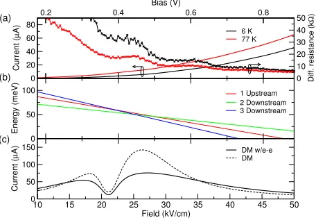
FIG. 7. (a) Experimental current and differential resistance. The positive polarity refers to positive bias applied to the top of the mesa and corresponds to electron injection from the left side in Fig. 6. (b) Calculated subband alignment ener-gies at 77 K. (c) Current calculated with the density matrix formalism with and without additional e-e dephasing at 77 K.
to those used for RTD simulations were used as both de-vices were grown in similar conditions. Additionally, the effect of electron–electron interactions is investigated by calculating current both with and without an additional dephasing rate, as was included in Section II.
B. Results
The experimental and calculated current are shown in Fig. 7(a) as a function of the applied electric field, along with the subband energy variation. Two strong alignment features are apparent in the simulated current. From our theoretical model it is deduced that these arise from the ground state of the 49 ˚A well coming into res-onance with the upstream states and downstream states at different biases. This behavior is less readily apparent in the experimental data, since the sequential tunnelling features are obscured by a large parasitic current, which is likely due to traps and other current paths associated with defects such as screw dislocations.64 However, the alignment features are clearly visible as plateaus in the differential resistance and there is excellent agreement between the experimental and simulated alignment volt-ages, indicating that effects of electric field domain for-mation are negligible on overall current. The I–V fea-tures are reproducible and do not show any evidence of hysteresis within the error of the measurements.
Fig. 6(b) shows that by doubling the contact doping,
nextnano3 predicts that residual bending near the end of the device can be suppressed by increased screening due to the ionized dopants. While interface charge effects do not have a significant effect on sequential tunnelling in
0 1 2 3 4 5 6 7 8
E0.5 (kV0.5/cm0.5) 0.01
0.1 1 10
J/E (A/kVcm)
[image:9.595.57.285.67.224.2]6 K 77 K
FIG. 8. Experimental sequential tunnelling current divided by electric field vs square root of electric field at 6 K and 77 K along with straight line fits.
the majority of the device, careful control of the doping and spacer layers is necessary for the most efficient overall electron transport and simulations suggest that contact doping should generally be as high as possible.
The effect of electron–electron scattering is to reduce and broaden the vertical electron transport as shown in Fig. 7(c) and this must be taken into account in superlat-tice doping considerations for optimized structures. Sim-ulations of the device at 6 K resulted in negligible I–V
differences compared with simulations at 77 K. This was unexpected since the experimental data shows a shift to lower resistance at higher temperatures. This discrep-ancy can be explained by the low lattice temperatures at which phonon scattering is insignificant, thus causing simulations to be similar at both temperatures. The ex-perimental decrease in resistance is then consistent with recent studies on the thermal activation of charge traps65 and resembles features of Frenkel–Poole tunnelling.37
[image:9.595.325.534.74.228.2]per-9
formed to minimize strain with balanced substrates.67,68
IV. CONCLUSIONS
In summary, we have studied the vertical electron transport in different types of AlGaN/GaN heterostruc-tures both theoretically and experimentally. Excellent agreement has been obtained between measured current– voltage characteristics and values calculated by the den-sity matrix formalism. This is a general approach, which can also be applied to QCL devices engineered to give optical gain, and is therefore a useful design and opti-mization tool. Fitted interface roughness values indicate high interface quality however sequential tunnelling de-vices were observed to have a significant parallel para-sitic current, likely due to defects. Our results indicate the feasibility of quantum devices such as QCLs provided defect density is reduced further and interface roughness is kept low.
ACKNOWLEDGMENTS
The authors are grateful to EPSRC (UK) for a DTG award and to the University of Leeds FIRC 2011 grant. Experimental work was supported by the NSF Award No. ECCS-1001431 and from the Defense Advanced Re-search Project Agency (DARPA) under Contract No. D11PC20027.
1R. K¨ohler, A. Tredicucci, F. Beltram, H. E. Beere, E. H. Linfield,
A. G. Davies, D. A. Ritchie, R. C. Iotti, and F. Rossi, Nature 417, 156 (2002).
2B. S. Williams, Nat. Photonics1, 517 (2007).
3L. Li, L. Chen, J. Zhu, J. Freeman, P. Dean, A. Valavanis,
A. Davies, and E. Linfield, Electron. Lett50, 309 (2014).
4S. Fathololoumi, E. Dupont, C. Chan, Z. Wasilewski, S.
Lafram-boise, D. Ban, A. M´aty´as, C. Jirauschek, Q. Hu, and H. C. Liu, Opt. Express20, 3866 (2012).
5A. W. M. Lee, Q. Qin, S. Kumar, B. S. Williams, Q. Hu, and
J. L. Reno, Appl. Phys. Lett.89, 141125 (2006).
6V. D. Jovanovi´c, D. Indjin, Z. Ikoni´c, and P. Harrison, Appl.
Phys. Lett.84, 2995 (2004).
7H. Yasuda, T. Kubis, I. Hosako, and K. Hirakawa, J. Appl. Phys.
111, 083105 (2012).
8W. Freeman and G. Karunasiri, Appl. Phys. Lett.102, 152111
(2013).
9B. Levine, J. Appl. Phys.74, R1 (1993).
10R. Tsu and L. Esaki, Appl. Phys. Lett.22, 562 (1973).
11R. C. Bowen, G. Klimeck, R. K. Lake, W. R. Frensley, and
T. Moise, J. Appl. Phys.81, 3207 (1997).
12B. R. Bennett, R. Magno, J. B. Boos, W. Kruppa, and M. G.
Ancona, Solid-State Electron.49, 1875 (2005).
13S. Golka, C. Pfl¨ugl, W. Schrenk, G. Strasser, C. Skierbiszewski,
M. Siekacz, I. Grzegory, and S. Porowski, Appl. Phys. Lett.88, 172106 (2006).
14E. Baumann, F. R. Giorgetta, D. Hofstetter, H. Wu, W. J. Schaff,
L. F. Eastman, and L. Kirste, Appl. Phys. Lett. 86, 032110 (2005).
15C. Bayram, Z. Vashaei, and M. Razeghi, Appl. Phys. Lett.96,
042103 (2010).
16Z. Vashaei, C. Bayram, and M. Razeghi, J. Appl. Phys.107,
083505 (2010).
17C. Bayram, Z. Vashaei, and M. Razeghi, Appl. Phys. Lett.97,
181109 (2010).
18Y. Shao, S. D. Carnevale, A. T. M. G. Sarwar, R. C. Myers, and
W. Lu, J. Vac. Sci. Technol., B31, (2013).
19D. Li, L. Tang, C. Edmunds, J. Shao, G. Gardner, M. J. Manfra,
and O. Malis, Appl. Phys. Lett.100, (2012).
20D. Li, J. Shao, L. Tang, C. Edmunds, G. Gardner, M. J. Manfra,
and O. Malis, Semicond. Sci. Technol.28, 074024 (2013).
21M. Boucherit, A. Soltani, E. Monroy, M. Rousseau, D. Deresmes,
M. Berthe, C. Durand, and J.-C. De Jaeger, Appl. Phys. Lett. 99, 182109 (2011).
22A. Kikuchi, R. Bannai, K. Kishino, C.-M. Lee, and J.-I. Chyi,
Appl. Phys. Lett.81, 1729 (2002).
23L. Yang, H. He, W. Mao, and Y. Hao, Appl. Phys. Lett. 99,
153501 (2011).
24F. F. Sudradjat, W. Zhang, K. Driscoll, Y. Liao, A.
Bhat-tacharyya, C. Thomidis, L. Zhou, D. J. Smith, T. D. Moustakas, and R. Paiella, Phys. Status Solidi C9, 588 (2012).
25S. Sakr, Y. Kotsar, M. Tchernycheva, E. Warde, N. Isac, E.
Mon-roy, and F. H. Julien, Appl. Phys. Express5, 052203 (2012).
26R. Songmuang, G. Katsaros, E. Monroy, P. Spathis, C. Bougerol,
M. Mongillo, and S. D. Franceschi, Nano Lett.10, 3545 (2010).
27L. Rigutti, G. Jacopin, A. D. L. Bugallo, M. Tchernycheva,
E. Warde, F. H. Julien, R. Songmuang, E. Galopin, L. Largeau, and J.-C. Harmand, Nanotechnology21, 425206 (2010).
28E. Li, Z. Cui, M. Liu, and X. Wang, Integr. Ferroelectr. 137,
134 (2012).
29S. D. Carnevale, C. Marginean, P. J. Phillips, T. F. Kent, A. T.
M. G. Sarwar, M. J. Mills, and R. C. Myers, Appl. Phys. Lett. 100, 142115 (2012).
30C. Gmachl, H. M. Ng, S.-N. George Chu, and A. Y. Cho, Appl.
Phys. Lett.77(2000).
31M. Tchernycheva, L. Nevou, L. Doyennette, F. H. Julien,
E. Warde, F. Guillot, E. Monroy, E. Bellet-Amalric, T. Rem-mele, and M. Albrecht, Phys. Rev. B73, 125347 (2006).
32C. Edmunds, L. Tang, M. Cervantes, M. Shirazi-HD, J. Shao,
A. Grier, A. Valavanis, J. D. Cooper, D. Li, G. Gardner, D. N. Zakharov, Z. Ikoni´c, D. Indjin, P. Harrison, M. J. Manfra, and O. Malis, Phys. Rev. B88, 235306 (2013).
33H. Machhadani, Y. Kotsar, S. Sakr, M. Tchernycheva,
R. Colombelli, J. Mangeney, E. Bellet-Amalric, E. Sarigiannidou, E. Monroy, and F. H. Julien, Appl. Phys. Lett. 97, 191101 (2010).
34D. Hofstetter, D. P. Bour, and L. Kirste, Appl. Phys. Lett.104,
241107 (2014).
35W. Terashima and H. Hirayama, Phys. Status Solidi C8, 2302
(2011).
36F. Sudradjat, W. Zhang, K. Driscoll, Y. Liao, A. Bhattacharyya,
C. Thomidis, L. Zhou, D. J. Smith, T. D. Moustakas, and R. Paiella, J. Appl. Phys.108, 103704 (2010).
37O. Mitrofanov and M. Manfra, J. Appl. Phys.95, 6414 (2004).
38D. N. Nath, Z. C. Yang, C.-Y. Lee, P. S. Park, Y.-R. Wu, and
S. Rajan, Appl. Phys. Lett.103, 022102 (2013).
39B. A. Biegel and J. D. Plummer, Phys. Rev. B54, 8070 (1996).
40F. Rossi, P. Poli, and C. Jacoboni, Semicond. Sci. Technol.7,
1017 (1992).
41K. L. Jensen and F. A. Buot, Phys. Rev. Lett.66, 1078 (1991).
42S. Sakr, E. Warde, M. Tchernycheva, and F. H. Julien, J. Appl.
Phys.109, 023717 (2011).
43M. Boucherit, A. Soltani, M. Rousseau, J.-L. Farvacque, and
J.-C. DeJaeger, J. Appl. Phys.112, 114305 (2012).
44G. Beji, Z. Ikoni´c, C. A. Evans, D. Indjin, and P. Harrison, J.
Appl. Phys.109, 013111 (2011).
45S. Birner, T. Zibold, T. Andlauer, T. Kubis, M. Sabathil, A.
Trel-lakis, and P. Vogl, IEEE Trans. Electron Devices 54, 2137 (2007).
46J. D. Cooper, A. Valavanis, Z. Ikoni´c, P. Harrison, and J. E.
Cunningham, J. Appl. Phys.108, 113109 (2010).
47A. Yariv, C. Lindsey, and U. Sivan, J. Appl. Phys. 58, 3669
48M. A. Talukder and C. R. Menyuk, New J. Phys. 13, 083027
(2011).
49H. Callebaut and Q. Hu, J. Appl. Phys.98, 104505 (2005).
50C. Weber, A. Wacker, and A. Knorr, Phys. Rev. B79, 165322
(2009).
51A. Valavanis, Z. Ikoni, and R. W. Kelsall, Phys. Rev. B77,
075312 (2008).
52C. Sanderson, “Armadillo: An open source C++ linear algebra
library for fast prototyping and computationally intensive exper-iments,” Tech. Rep. (NICTA, Australia, 2010).
53E. Anderson, Z. Bai, J. Dongarra, A. Greenbaum, A.
McKen-ney, J. Du Croz, S. Hammerling, J. Demmel, C. Bischof, and D. Sorensen, inProceedings of the 1990 ACM/IEEE Conference
on Supercomputing, Supercomputing ’90 (IEEE Computer
Soci-ety Press, Los Alamitos, CA, USA, 1990) pp. 2–11.
54R. Terazzi, T. Gresch, A. Wittmann, and J. Faist, Phys. Rev. B
78, 155328 (2008).
55A. Fediai and V. Moskaliuk, inElectronics and Nanotechnology
(ELNANO), 2013 IEEE XXXIII International Scientific
Con-ference, Ukraine(2013) pp. 107–111.
56I. Abramov, N. Kolomeitseva, and I. Romanova, Russ.
Microlec-tron.41, 314 (2012).
57P. Zhao, H. L. Cui, D. Woolard, K. L. Jensen, and F. A. Buot,
J. Appl. Phys.87, 1337 (2000).
58A. Sakurai and Y. Tanimura, J. Phys. Soc. Jpn. 82, 033707
(2013), 1302.1076.
59J. B. Khurgin, Y. Dikmelik, P. Q. Liu, A. J. Hoffman, M. D.
Escarra, K. J. Franz, and C. F. Gmachl, Appl. Phys. Lett.94, 091101 (2009).
60C. W. I. Chan, Q. Hu, and J. L. Reno, Appl. Phys. Lett.103,
151117 (2013).
61E. Dupont, S. Fathololoumi, Z. R. Wasilewski, G. Aers, S. R.
Laframboise, M. Lindskog, S. G. Razavipour, A. Wacker, D. Ban, and H. C. Liu, J. Appl. Phys.111, 073111 (2012).
62Y. Hou, W.-P. Wang, N. Li, W. Lu, and Y. Fu, J. Appl. Phys.
104, 074508 (2008).
63T. V. Dinh, A. Valavanis, L. J. M. Lever, Z. Ikoni´c, and R. W.
Kelsall, Phys. Rev. B85, 235427 (2012).
64S. J. Pearton, J. C. Zolper, R. J. Shul, and F. Ren, J. Appl.
Phys.86, 1 (1999).
65S. Sakr, E. Warde, M. Tchernycheva, L. Rigutti, N. Isac, and
F. H. Julien, Appl. Phys. Lett.99, 142103 (2011).
66A. M. Katzenmeyer, F. Lonard, A. A. Talin, P.-S. Wong, and
D. L. Huffaker, Nano Lett. 10, 4935 (2010), pMID: 21053980, http://dx.doi.org/10.1021/nl102958g.
67K. Berland, T. G. Andersson, and P. Hyldgaard, Phys. Rev. B
84, 245313 (2011).
68V. Jovanovi´c, Z. Ikoni´c, D. Indjin, P. Harrison, V. Milanovi´c,