Abstract—In this paper, an analytical investigation of a new
graphene-based sensor called Dielectric Modulated Graphene Field Effect Transistor (DMG-FET), for high-performance biomolecule sensing applications, is developed and confirmed with numerical simulations. Transport drift-diffusion-based approach is used to develop the analytical models in order to study the DMG-FET behavior. The sensitivity of the proposed design is compared with that of conventional FET-based sensors. It has been shown that the proposed sensor has better electrical and scaling performance in comparison with the conventional design. This result makes the proposed design as a promising candidate to serve as a highly sensitive low-power and reliable graphene-based sensing applications. For that reason, the dielectric- modulated Graphene FET (DMGFET) provides a practical approach towards biomolecular detection that could be extended to other applications.
Index Terms— biomolecule sensing, dielectric, grapheme,
sensitivity.
I. INTRODUCTION
ecently, the Ion Sensitive FETs (ISFETs) sensors attract much attention in reliable and high performance applications for engineering and medical applications due to their reliability, low power consumption, non-destructive read-out of chemical and electrical information, high molecule detection range, and compatibility to standard CMOS technology [1-3]. However, with the progression of microelectronic industry and the increasing of the sensor performances, control of parasitic parameters and improvement of the sensor reliability against the biological and chemical variation of the neutral molecules are the biggest challenges in future embedded electronic systems for sensing and monitoring applications. Therefore, new design and materials should be developed in order to overcome these challenges. In this context, the use of Graphene-based material to design and fabricate these sensors may be considered as alternative for high performance and reliable monitoring applications. The importance of Graphene-based material is rising in microelectronic industry. This is mainly due to the low manufacturing costs of planar graphene and its excellent F. Djeffal is with the Laboratory of Advanced Electronic, Department of Electronics, LEPCM, University of Batna, 05000, Algeria (e-mail: [email protected], [email protected]).
K. Tamersit is with the Laboratory of Advanced Electronic, Department of Electronics, University of Batna, 05000, Algeria (e-mail: [email protected]).
M. Meguellati is with the Laboratory of Advanced Electronic, Department of Electronics, University of Batna, 05000, Algeria (e-mail: m_meguellati @yahoo.fr).
electronic properties. Recently, several investigations have been proposed to analyze the Graphene-based devices and to make us better understanding of its physics behavior [4-6].
Dielectric modulated field effect transistors (DMFETs) are rising as a significant device for microelectronic applications due to its high saturation velocity, high carrier mobility and excellent charge transport [7-9]. Several works have investigated these devices [7-9]. However, these works have only been focused on studding the experimental aspects of these devices for silicon-based materials, where the analytical analysis, design methodologies and sensitivity behavior have not been taken into account, thus limiting the models and structures used by designers. Therefore, new analytical, materials and design approaches which capture and improve the sensitivity behavior, for high-performance biomolecule sensing applications, should be developed in order to build a complete graphene-based bimolecular sensor compact model and improved design for medical and engineering applications [11,12].
In this work, an analytical investigation of a new graphene-based sensor, for high-performance biomolecular sensing applications, is developed and confirmed by experimental validation. The sensitivity of the proposed design is compared with that of conventional Silicon (Si) FET-based sensors. It has been shown that the proposed sensor has better electrical and scaling performance in comparison with the conventional (Si) FET-based sensor.
II. ANALYTICALANALYSIS
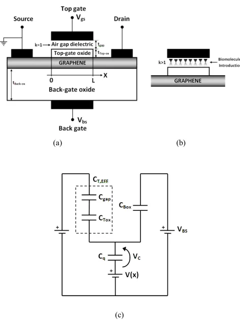
The present investigation suggests a new design called Dielectric Modulated Graphene Field Effect Transistor (DMG-FET) for high-performance biomolecule sensing applications, where the Dielectric region is introduced between the gate and the top-gate oxide. In Figure.1 (a and b), we show the cross sections of the proposed DMG-FET design. As it is shown in this figure, the detection is performed by the presence of air gap dielectric between the top gate and top-gate oxide.
Using an equivalent circuit analogy, a DMG-FET device can be represented by the Figure. 1c.
From the equivalent capacitive circuit, CT,EFF and CBox are the effective top gate capacitance (CTox in series with Cgap) and the bottom oxide capacitance respectively.
where:
) t t
/(
CT,EFF Top-oxgap gap Top-oxTop-ox gap
Cq represents the quantum capacitance of graphene. C
q kV
C
Analytical Analysis of a New Graphene-based
Sensor for High-performance Biomolecule
Sensing Applications
F. Djeffal, Member, IAENG, K. Tamersit, and M. Meguellati, Member, IAENG
(a) (b)
[image:2.595.51.287.58.375.2](c)
Figure 1. (a) cross section view of the double gate GFET transistor with air gap dielectric for the biodetection before the biomolecule binding. (b) Cavity after biomolecules introduction. (c) Equivalent capacitive circuit of
the graphene-based biotransistor.
where: k (2q / )(q/( vF)2)
2
and vF(106m/s)
is the Fermi velocity. The expression of Cq is convincing under the conditionqVC kBT .
The potential V(x)is the voltage drop in the graphene channel, which is equals to zero at the source end (x0)
and equals to the drain–source voltage Vds at the drain end
) L x
( .
The overall net mobile sheet charge density in the graphene channel is defined [11] as
C q C q(p n) (1/2)CV
Q
where q Box EFF , T Box q Box EFF , T EFF , T GS C C 2 1 C C C )) x ( V VBS ( C 2 1 C C C )) x ( V V ( ) x ( V
with VGS VgsVgs0and VBS VbsVbs0are the top and back gate–source voltage overdrives, respectively.
velocity in the channel. This later can be expressed as,
) vsat / E 1 /( E
v where vsatis the saturation velocity, E and µ represent the applied electric field and carrier mobility in the channel, respectively.
After some mathematical manipulations, the subthreshold current derived for our design can be expressed [13] as
ds ds V 0 sat V 0 C DS dV v 1 L dV W q I
where L represents the channel length. The subthreshold current derived for our design leads to:
CD CS CD CS V V C C C sat V V C C C C DS dV dV dV ) V ( v 1 L dV dV dV ) V ( W q I
where VCis obtained from the expression of the channel potential, VC(x). This latter can be written as:
k C ) V VBS ( C C qN V VGS k 2 ) C C ( ) C C ( V Box EFF , T EFF , T f 2 Box EFF , T Box EFF , T C
where k is a constant, which takes a positive or negative
sign, when
) 0 ( 0 C ) V VBS ( C C qN V
VGS T,EFF Box
EFF , T f , respectively.
Also, both the channel potential at the source and drain sides VCSand VCD are determined by VC(V0)and
) V V (
VC ds , respectively. Moreover, the expression of
) x (
VC leads to:
1 kV sgn(V )/(C C )
dV /
dV C C C T,EFF Box , and
0 2
C C
C(V ) kV /(2q)
From this latter, we can calculate the final subthreshold drain current model as,
(sgn(V )V sgn(V )V )
) C C ( 8 k ) V V ( 6 k V q L W
I CS CS4
4 CD CD Box EFF , T 2 3 CS 3 CD ds 0 eff
DS
0,0 -0,5 -1,0 -1,5 -2,0 0,0
-0,2 -0,4 -0,6 -0,8 -1,0 -1,2 -1,4
.
+ +
+ + +
+
.
.
.
.
.
.
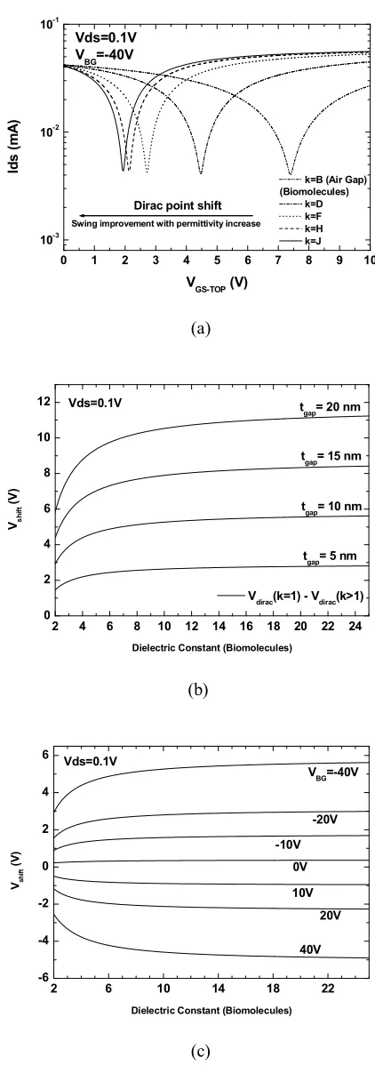
Analytical model (Symbols) Experimental results [15]
I
d
s
(
m
A
)
Vds-ext (V)
.
+
Vgs = - 1.25 V - 0.75 V
+0.75 V
+0.25 V - 0.25 V
[image:3.595.315.526.62.661.2]
Figure 2. Output characteristics obtained from the analytical model compared with experimental results.
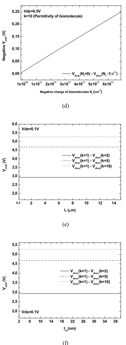
Figure.3 plots the proposed sensor behavior as function of different geometrical and electrical parameters. The impact of different parameters on the sensor sensitivity is also presented in this figure. Figure.3a shows the impact of the variation of the dielectric constant on the output I-V characteristics, where the shift of the Dirac-point in the negative direction is well observed. This shift is due to the increasing of the dielectric constant, which is mainly depends on the nature and the variation of biomolecular concentration. it is to note the that the main parameter which affects the shift in the Dirac-point is the top capacitance (CEFF). Figure.3b shows the variation of Vshift as function of dielectric constant for different nano-gap (cavity) values. It is shown that the increasing of the cavity width leads to an increasing in the sensitivity. Figure.3c plots the variation of Vshift as function of dielectric constant for different applied gate voltage values. It is clearly shown that Vshift is mainly depends on the applied gate voltage values, where its value increases when the applied voltage is increased. Therefore, high applied gate voltage is needed in order to obtain high sensor performances. Figure.3d shows the shift of the Dirac-point as function of negative biomolecule charges Nf located in the cavity region. For the proposed design, the output response of the sensor is linear with absorbed biomolecules concentration. It is clearly observed that DMG-FET has higher sensitivity. This means that DMG-FET has better electrical and scaling performances. From Figures 3a and 3b, we can observe that the sensor sensitivity cannot be affected by the channel length and the oxide thickness. It is to note that the same phenomenon can be observed for the impact of top-oxide dielectric constant.
0 1 2 3 4 5 6 7 8 9 10
10-3
10-2
10-1
Vds=0.1V V
BG=-40V
Id
s
(
m
A
)
VGS-TOP (V)
k=B (Air Gap) (Biomolecules)
k=D k=F k=H k=J
Swing improvement with permittivity increase Dirac point shift
(a)
2 4 6 8 10 12 14 16 18 20 22 24
0 2 4 6 8 10
12 Vds=0.1V
tgap= 5 nm
tgap= 10 nm
tgap= 15 nm
Vs
h
if
t
(
V
)
Dielectric Constant (Biomolecules)
Vdirac(k=1) - Vdirac(k>1)
tgap= 20 nm
(b)
2 6 10 14 18 22
-6 -4 -2 0 2 4 6
40V 20V 10V 0V -10V
Vs
h
if
t
(
V
)
Dielectric Constant (Biomolecules)
VBG=-40V
-20V Vds=0.1V
[image:3.595.60.275.70.225.2]1x10¹⁰ 1x10¹¹ 2x10¹¹ 3x10¹¹ 4x10¹¹ 5x10¹¹ 6x10¹¹ 0,00
0,05 0,10 0,15 0,20
0,25 Vds=0.5V
k=10 (Permitivity of biomolecule)
N
e
g
a
ti
v
e
Vs
h
if
t
(
V
)
Negative charge of biomolecules N
f(cm -2
) V
dirac(Nf=0) - Vdirac(Nf -1
)
(d)
2 4 6 8 10 12 14
2,0 2,5 3,0 3,5 4,0 4,5 5,0 5,5 6,0
Vds=0.1V
V
dirac(k=1) - Vdirac(k=2)
Vdirac(k=1) - Vdirac(k=5) Vdirac(k=1) - Vdirac(k=10)
Vs
h
if
t
(
V
)
L (m)
0.2
(e)
2 6 10 14 18 22 26 30 34 38
2,0 2,5 3,0 3,5 4,0 4,5 5,0 5,5
Vds=0.1V
Vdirac(k=1) - Vdirac(k=2) Vdirac(k=1) - Vdirac(k=5) Vdirac(k=1) - Vdirac(k=10)
Vsh
if
t
(
V)
tox(nm)
(f)
of the biomolecules concentration (Nf) can be carried out by using a simple Read-out Circuit (RC), in which the threshold voltage is measured at a single point of the transfer characteristics, applying a specified current (in the order of ten μA) to the sensor. Due to the simplicity of the Read-out Circuit, the RC configuration is suitable for practical low power applications
IV. CONCLUSION
In this paper, an analytical investigation of a new graphene-based sensor called Dielectric Modulated Graphene Field Effect Transistor (DMG-FET), for high-performance biomolecule sensing applications, is proposed. An analytical analysis comprising biomolecules concentration effect, drain current, threshold voltage shift and sensitivity behavior for DMG-FET has been developed. The sensitivity of the proposed has been investigated, and the impacts of variation in geometrical and electrical parameters have also studied. It is found that the sensitivity of the device can be increased by increasing the cavity thickness and the applied gate voltage. This result can be explained by the excellent sensitivity of the graphene against the variation of the top-electrostatic capacitance. The obtained results make DMG-FET a promising candidate for submicron, sensitive, low power, and reliable graphene-based biosensor.
REFERENCES
[1] F. Djeffal, D. Arar, M.A. Abdi, R. Mahamdi and A. Errachid, “A multigate design to improve the electrical performance for deep submicron ISFET-based sensors,” Sensor Letters, Vol. 9, pp. 2309-2311, 2011.
[2] B. Gu, T.J. Park, J.-H. Ahn, X.-J. Huang, S.Y. Lee, and Y.-K. Choi, “Nanogap field-effect transistor biosensors for electrical detection of avian influenza,” Small, vol. 5, pp. 2407-2412, 2009.
[3] S. Kim, J.-H. Ahn, T.J. Park, S.Y. Lee, and Y.-K. Choi, “A biomolecular detection method based on charge pumping in a nanogap embedded field-effect-transistor biosensor,” Appl. Phys. Lett., vol. 94, pp. 243903-1 - 243903-3, 2009.
[4] R. Narang, K.V.S. Reddy, M. Saxena, R.S. Gupta, and M. Gupta, “A dielectric-modulated tunnel-FET-based biosensor for label-free detection: Analytical modeling study and sensitivity analysis,” IEEE Trans. Electron Devices, vol. 59, pp. 2809-2817, 2012.
[5] J. G. Champlain, “A first principles theoretical examination of graphene based field effect transistors,” J. Appl. Phys., vol. 109, pp. 084515-1 - 084515-19, 2011.
[6] S. Kim, D. Baek, J.-Y. Kim, S.-J. Choi, M.-L. Seol, and Y.-K. Choi, “A transistor-based biosensor for the extraction of physical properties from biomolecules,” Applied Physics Letters, vol. 101, pp. 073703-1 - 073703-4, 2012.
[7] J.M. Choi, J.W. Han, S.J. Choi, and Y. K. Choi, “Analytical modeling of a nanogap-embedded FET for application as a biosensor,” IEEE Trans. Electron Devices, vol. 57, no. 12, pp. 3477–3484, Dec. 2010. [8] D. Jimenez and O. Moldovan, “Explicit drain-current model of
[image:4.595.57.274.66.656.2][12]K. Tamersit, F. Djeffal, D. Arar and M. Meguellati, Analytical Investigation of Subthreshold Swing to Study the Scaling Capability of Graphene Field- effect Transistors, accepted, World Congress On Engineering 2013, WCE 2013, July 3 -5, 2013, London, U.K. [13]C.-H. Kim, C. Jung, H.G. Park, and Y.-K. Choi, “Novel dielectric
modulated field-effect transistor for label-free DNA detection,” Biochip J., vol. 2, no. 2, pp. 127–134, Jun. 2008.
[14]X. Chen, Z. Guo, G.-M. Yang, J. Li, M.-Q. Li, J.-H. Liu, and X.-J. Huang, “Electrical nanogap devices for biosensing,” Mater. Today, vol. 13, no. 11, pp. 28–41, Nov. 2010.