Abstract -- A FPGA Implementation of a bilateral filter for image processing is given which does spatial averaging without smoothing edges. Kernel based processing is possible, which means that processing of the entire filter window at one pixel clock cycle. It is also supported by the arrangement of the input data into groups and applied a single clock cycle for a group of pixels. Based on these features, a technique called Error Tolerant Adder (ETA) is implemented in Bilateral Filter to minimize Power Delay Product (PDP). ETA provides high accuracy and achieves both power consumption and average case performance.Furthermore, ETA to eliminate the carry propagation path and improve the speed.The ETA can be expanded to a proposed addition arithmetic in which the conventional adder is divided into two parts. In Bilateral Filter a kernel of different size can be implemented using ETA whichachieves good performance.
Index Terms -- Bilateral filter, ETA, Image processing, noise reduction, PDP.
I. INTRODUCTION
BILATERAL FILTER has a feature of noise reduction, in addition to improve the visual quality and allows improving the compressibility of the image. Bilateral filter [1] consists of two types. First one is non linear component, second one is linear component. If both the types are adjusted to reduce the noise via selective averaging and the amount of blurring via low pass filter. The bilateral filter is applied for noise reduction for local tone mapping method [2], which maps high dynamic range image to low dynamic range image. The bilateral filter can be used to medical image processing [3] and non-destructive testing. The detailed description of a paper, bilateral filter based on Register Transfer Level (RTL). The advantages of bilateral filter,
1) The input data are divided into equal groups to assigned individual pipelines.
2) To increase the internal clock frequency based on Data flow
3) Reduce the external memory storage.
Various technique have been developed for reducing the power consumption of VLSI designs, including voltage scaling, switched capacitance reduction, power down techniques, dynamic voltage frequency scaling[4]-[7]. ETAto provide high accuracy and achieves both power consumption and average case performance. The concept of ETA defined in two categories, the first one category it contains defects that
Manuscript received March, 2015
S.Anitha,PGStudent, Kalasalingam Institute of Technology. Email id: [email protected]
V.Muneeswaran, PGStudent, Kalasalingam Institute of Technology.
J.Jayaseeli Pratheepa, PGStudent, Kalasalingam Institute of Technology.
B.Hema, Assistant Professor, Kalasalingam Institute of Technology. Email id: [email protected].
cause internal and external errors, [8]-[10] the second category, that system incorporates this circuit produce an acceptable results
In previous Works, many high quality interpolation based methods have been [11] proposed. Image scaling algorithm, cost of hardware and memory also reduced. For real time applications, less complexity image scaling processor algorithms are needed for VLSI implementations [12] – [13].
II.BILATERAL FILTER
Bilateral filter[1] is an edge preserving and noise reducing smoothing filter for images. The intensity value at each pixel of an image is replaced by a weighted average of intensity value from nearbypixel.
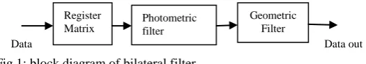
Fig 1: block diagram of bilateral filter
Bilateral filter is a combination of linearand non linear component. The bilateral filter is subdivided into three parts. Three parts are register matrix, photometric filter, geometric filter. Fig.1 presents three parts and their order in the concept. First the image is converted into pixel value. The pixel value is given into the register matrix. It reads the data line by line and arranged for further processing in Register matrix. The second part isthe photometricfilter, which weights the input data according to the intensity of the processed pixels. The filtering process completed by the geometric filter, and the final output marked by “Data_out”.
(a) Register matrix:
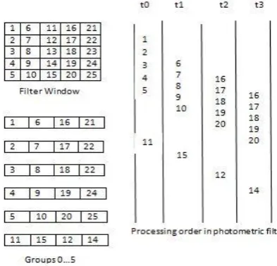
In register matrix fig.2 kernel based design concept is applied. As the pixel value is shifted from one stage
to next stage simultaneously.It processes all 25 pixels in one pixel cycle in order to keep reading of the input lines into the register matrix. The output of the register matrix is sorted into six groups for one cycle, fed into the photometric filter component with the quadruple clock frequency synchronously. Quadruplication means four pixels per clock signal.
(b) Photometric filter:
After the register matrix process completed, the six grouped image data are applied to the photometric filter component fig.3. In photometric filter look up table created by using photometric coefficients. The photometric coefficients calculated by using this formula,
S(ø(m0),ø(m)=exp((-0.5)( ІІø(m0)-ø(m) ІІ/σ ph)2
To avoid the calculation of the expensive exponential, all possible values of the function precalculated and stored in the LUT [14]. The difference of the gray values calculated and directly interpreted as the address of the corresponding weight coefficient in the LUT.
Analysis of low PDP using ETA in bilateral filter
S.Anitha, V.Muneeswaran, J.Jayaseeli Pratheepa , B.Hema
Register
Matrix Photometric filter
Geometric Filter Data
in
Fig 2: Register matrix of the kernel-based Design
If the gray value difference is greater than the limit, the weight coefficients set to zero otherwise corresponding coefficients readout the LUT.
(c) Geometric filter:
Separabilty and symmetry property can be used for geometric filter component. Because of the separabilty, the geometric filter is split into vertical and horizontal parts. The geometric coefficients can be calculated by using this formula,
C (m0, m) =exp ((-0.5) (ІІm0-mІІ /σ c) 2
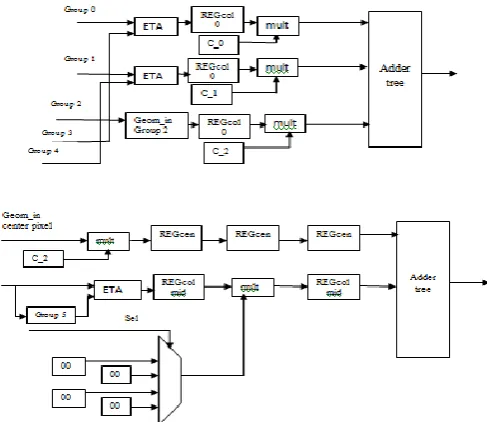
The coefficients of the geometric component are labelled “C_0, C_1, and C_2”. Due to the symmetry of the weight coefficients of the geometric component, the order of multiplication and addition is swapped in both the filter parts.
Fig 3: block diagram of photometric filter
C.1 Vertical component part:
The output of photometric filter is coefficients, mid_pix; pixel weights are given to the geometric filter. The groups 0,1,3,4,5 and mid_pix 2 are processed as shown fig 5. The geometrically symmetrical pixels are accumulated at first and then multiplied by geometric weight ccoefficients. In this method the binary adder can be replaced by SPST adder.
Fig4: Processing order in photometric filter
Fig 5: vertical part of the geometric filter Component
Fig 6: Horizontal part of the geometric filter Component
C.2 Horizontal component part:
After processing in the vertical dimension, the filter window is reduced to one row, and its elements are computed at one internal clock event each. In order to able to reuse the symmetrical design, the values of the filtered columns 0, 1, 2, 3, 4 are stored in the shift registers scoring to the order of their reception.
Fig7: block diagram of ETA
III.ERROR-TOLERANT ADDER
In this paper some common definitions can be used.
Overall error (OE) : It is represented by | Rc-Re|, Rc denotes thecorrect result and Re denotes the result obtained by adder. Accuracy (ACC) : In this technique, the accuracy of an adder is used to indicate how “correct” the output of an adder is for a particular input.
Minimum Acceptable Accuracy : In this method used to adjust the threshold value. The result obtained whose accuracy is higher than the minimum acceptable accuracy is called acceptable result.
Need for ETA:
Increasingly huge data sets and the need for instant response require the adder to be large and fast. The traditional RCA and CLA no longer suitable for large adder because of this
low speed performance. So ETA sacrificing some accuracy, the ETA can attain great improvement in both the power consumption and speed performance.
Fig8: example for spurious computations IV. PROPOSED ETA\\\\\\
The conventional adder circuit, the delay is mainly attributed to the carry propagation chain along the critical path, from the LSB to MSB. In this adder the glitches are caused by carry propagation path [15]-[16]. To eliminate the carry propagation path the new adder can be proposed. First the input operands divide into two types. 1. Accurate part, 2.Inaccurate part. The accurate part consists of several higher order bits and the in accurate part consists of remaining lower order bits. The accurate part considers normal addition operation can be performed. Inaccurate part consider some conditions can be followed, I) if both the inputs are 0 or different normal addition operation performed. ii) Both the inputs are 1 all proceeding bits are set to be 1. The inaccurate part consists of carry free addition block and the control block. The control block is used to generate the control signals, to determine the working mode of the carry – free addition block. Overall architecture of carry-free addition block. The carry free addition block is made up of 20 modified XOR gates, and each of which is used to generate the sum bit. By eliminating the carry propagation path in the inaccurate part and performing the addition in two separate parts simultaneously, the overall delay time greatly reduced, so is the power consumption.
Fig 9: ETA using Geometric Filter
1 0 1 1 0 0 1 1 1 0 0 1 1 0 1 0 0 1 1 0 1 0 0 1 0 0 0 1 0 0 1 1
1 0 0 0 1 1 1 0 0 1 0 0 1 1 1 1 1
Fig8 : Proposed addition arithmetic
Accurate part Inaccurate part
.
Fig10: overall architecture of carry free addition block and control block
V.SIMULATION RESULTS
The test image eye shown in FIG. Is an 8-b gray scale image with size of 85 *85 pixelsHence, in the following, GVmax = 255 are used. The bilateral filter was implemented in VHDL and simulated with modelsim. The PDP was simulated using Xilinx. A test image was filtered by Matlab implementations as well as the Modelsim simulation, and the filtered images were compared. The total delay of the output pixels of our architecture with a kernel size of 5*5 pixels applied to an image of 85*85 pixels is 7225 cycles.
Input image
Modelsim output image
In register matrix 5 *5 kernel size pixels are being processed. Finally, the output of the register matrix is sorted into 5 groups and center pixel value is seperately obtained.
The output of the register matrix is given to tha photometric filter. In photomtric filter Look Up Table can be created and the photometric coefficients are got. By multiplying the photometric coefficient and group value we can get a weighted coefficients.
The output of photometric filter is given to the geometric filter. In this filter, vertical part and horizontal part
Mat lab output image
process is done seperately. The vertical part component carried out weighted coefficients and horizontal component part carried out photometric coefficients.
Each 5 *5 pixels to calculate the power, area, delay, which compare normal binary adder and ETA adder.
Table1: power consumption of proposed SPST
VI. CONCLUSION
In this paper, the ETA technique was proposed to minimize area, power and delay. ETA adder, which provides better performance improvement with a slight accuracy loss. The bilateral filter architecture assures a constant processing delay, independent of the filter window size. The total consumed power for this technique is 101 mW which is 40.58% power reduction when compared to binary adder technique.
References
[1]C. Tomasi and P. Manduchi, “Bilateral filtering for gray and color images,” in Proc. IEEE ICCV, 1998, pp. 839–846.
[2] J. Won Lee, R.-H. Park, and S. Chang, “Noise reduction and adaptivecontrast enhancement for localtone mapping,” IEEE
Trans. Consum.Electron., vol.58, no. 2, pp. 578–586, May 2012.
[3] J. Giraldo, Z. Kelm, L. Yu, J. Fletcher, B. Erickson, and C. McCollough,“Comparative study of two image space noise reduction methods for computedtomography: Bilateral filter and nonlocal means,” in Proc. ConfIEEE EMBS, 2009, pp. 3529–3532. [4] A. Bellaouar and M. I. Elmasry, Low-Power Digital VLSI
Design"Circuits and Systems. Norwell, MA: Kluwer, 1995.
[5] A. P. Chandrakasan and R. W. Brodersen, “Minimizing power consumption in digital CMOS circuits,” Proc. IEEE, vol. 83, no. 4, pp. 498–523, Apr. 1995.
[6] K. K. Parhi, “Approaches to low-power implementations of DSP systems,”IEEE Trans. Circuits Syst. I, Fundam. Theory
Appl., vol. 48, no.pp. 1214–1224, Oct. 2001.
[7] K. Choi, R. Soma, and M. Pedram, “Dynamic voltage and frequencyscaling based on workload decomposition,” in Proc.
IEEE Int. Symp.LowPower Electron.Des., 2004, pp. 174–179.
[8] K. V. Palem, “Energy aware computing through probabilisticswitching: A study of limits,” IEEE Trans. Comput., vol. 54, no. 9, pp.1123–1137, Sep. 2005.
[9] S. Cheemalavagu, P. Korkmaz, and K. V. Palem, “Ultra low energy computing via probabilistic algorithms and devices: CMOS device primitives and the energy probability relationship,” in Proc.
2004 Int.Conf. Solid State Devices and Materials, Tokyo, Japan,