University of New Orleans University of New Orleans
ScholarWorks@UNO
ScholarWorks@UNO
University of New Orleans Theses and
Dissertations Dissertations and Theses
5-18-2007
Embedded Multilayer Thin Film Stacks as Polarizing Beam
Embedded Multilayer Thin Film Stacks as Polarizing Beam
Splitters and Wave Retarders Operating under Condition of
Splitters and Wave Retarders Operating under Condition of
Frustrated Total Internal Reflection
Frustrated Total Internal Reflection
Perla Siva Reddy
University of New Orleans
Follow this and additional works at: https://scholarworks.uno.edu/td
Recommended Citation Recommended Citation
Reddy, Perla Siva, "Embedded Multilayer Thin Film Stacks as Polarizing Beam Splitters and Wave Retarders Operating under Condition of Frustrated Total Internal Reflection" (2007). University of New Orleans Theses and Dissertations. 1079.
https://scholarworks.uno.edu/td/1079
This Dissertation is protected by copyright and/or related rights. It has been brought to you by ScholarWorks@UNO with permission from the rights-holder(s). You are free to use this Dissertation in any way that is permitted by the copyright and related rights legislation that applies to your use. For other uses you need to obtain permission from the rights-holder(s) directly, unless additional rights are indicated by a Creative Commons license in the record and/ or on the work itself.
Embedded Multilayer Thin Film Stacks as Polarizing Beam Splitters and Wave Retarders Operating under Condition of Frustrated Total Internal Reflection
A Dissertation
Submitted to the Graduate Faculty of the University of New Orleans in partial fulfillment of the requirements for the degree of
Doctor of Philosophy in
Engineering and Applied Science Electrical Engineering
by
Siva Reddy Perla
B. Tech. Jawaharlal Nehru Technological University, 2001 M. S. University of New Orleans, 2003
ACKNOWLEDGEMENTS
TABLE OF CONTENTS
List of Tables ... iv
List of Figures ...v
Abstract... vi
1. Introduction...1
2. Review of literature...2
2.1. Polarizing beam splitters...2
2.2. Wave retarders ...3
3. Design procedure ...4
3.1. Centro-symmetric multilayer stacks ...4
3.1.1. Polarizing beam splitters...6
3.1.2. Complete transmission QWR and HWR devices ...8
3.1.3. 50%-50% beam splitters ...10
3.2. Periodic multilayer stacks ...12
4. Results...16
4.1. Centro-symmetric multilayers as PBS...16
4.1.1. Angular sensitivity...19
4.1.2. Spectral sensitivity...22
4.2. Centro-symmetric multilayers as transmission wave retarders ...25
4.2.1. QWR using SiO2-Si multilayer embedded in GaP prism ...25
4.2.2. HWR using SiO2-Si multilayer embedded in Si prism...29
4.3. Centro-symmetric multilayers as 50%-50% beam splitters...31
4.3.1. 50%-50% beam splitters with Δr= 0o and Δt= 0o...34
4.3.2. 50%-50% beam splitters with Δr= 0o and Δt= 180 o...36
4.3.3. 50%-50% beam splitters with Δr= 180o and Δt= 0o...37
4.3.4. 50%-50% beam splitters with Δr= 180o and Δt= 180o...39
4.3.5. 50%-50% beam splitters with Δr= ±90o and Δt= ±90o...40
4.4. Periodic multilayers as polarizers and PBSs...41
4.4.1. PBS using BaF2-PbTe multilayer embedded in ZnS prism ...42
4.4.2. Angular sensitivity...48
4.4.3. Spectral sensitivity...58
5. Summary and Conclusions ...69
References...70
List of Tables
Table 1: List of various 50%-50% beam splitters...12
Table 2: Normalized and metric thicknesses for centro-symmetric PBS ...19
Table 3: Discrete polarizing angles in Panel A1 of Fig. 8 ...21
Table 4: Discrete polarizing wavelengths of Fig. 10 ...24
Table 5: Normalized and metric thicknesses for transmission QWR and HWR...27
Table 6: 50%-50% beam splitters cube designs ...32
Table 7: Normalized and metric thicknesses for 50%-50% beam splitters ...34
Table 8: Normalized and metric thicknesses for periodic multilayer PBS...48
Table 9: Discrete polarizing angles in Figs. 26-31 ...55
List of Figures
Figure 1: Centro-symmetric multilayer PBS ...6
Figure 2: Centro-symmetric multilayer transmission retarder...8
Figure 3: Centro-symmetric multilayer 50%-50% beam splitter...10
Figure 4: Periodic multilayer PBS ...12
Figure 5: Z2 vs Z1 plots for 3-, 7- and 11-layer designs ...16
Figure 6: Z2 vs Z1 plots for 15-layer design ...17
Figure 7: Z2 vs Z1 plots for 19-layer design ...18
Figure 8: ERr, ERt vs φ0 for 3-, 7-, 11-, 15- and19-layer designs...20
Figure 9: |Rp|2, |Rs|2 vs φ0 for 3-, 7-, 11-, 15- and19-layer designs...22
Figure 10: ERr, ERt vs λ for 3-, 7-, 11-, 15- and19-layer designs...23
Figure 11: |Rp|2, |Rs|2 vs λ for 3-, 7-, 11-, 15- and19-layer designs ...25
Figure 12: Spectral and angular response for transmission QWR...26
Figure 13: Thickness error sensitivity for transmission QWR ...28
Figure 14: Spectral and angular response for transmission HWR...29
Figure 15: Thickness error sensitivity for transmission HWR ...31
Figure 16: Spectral and angular response for 50%-50% BS; Δr= 0o and Δt= 0o...35
Figure 17: Spectral and angular response for 50%-50% BS; Δr= 0o and Δt= 180o...37
Figure 18: Spectral and angular response for 50%-50% BS; Δr= 180o and = 0 t Δ o...39
Figure 19: Spectral and angular response for 50%-50% BS; Δr= 180o and Δt= 180o....41
Figure 20: Z2 vs Z1 plots for 4-, 6- and 8-layer designs ...42
Figure 21: Z2 vs Z1 plots for 10-layer design ...43
Figure 22: Z2 vs Z1 plots for 12-layer design ...44
Figure 23: Z2 vs Z1 plots for 14-layer design ...45
Figure 24: Z2 vs Z1 plots for 16-layer design ...46
Figure 25: Z2 vs Z1 plots for 18-layer design ...47
Figure 26: |Rp|2, |Rs|2 vs φ0 for 4-, 6- and 8-layer designs ...49
Figure 27: |Rp|2, |Rs|2 vs φ0 for 10-layer design ...50
Figure 28: |Rp|2, |Rs|2 vs φ0 for 12-layer design ...51
Figure 29: |Rp|2, |Rs|2 vs φ0 for 14-layer design ...52
Figure 30: |Rp|2, |Rs|2 vs φ0 for 16-layer design ...53
Figure 31: |Rp|2, |Rs|2 vs φ0 for 18-layer design ...54
Figure 32: |Rp|2, |Rs|2 vs λ for 4-, 6- and 8-layer designs ...59
Figure 33: |Rp|2, |Rs|2 vs λ for 10-layer design ...60
Figure 34: |Rp|2, |Rs|2 vs λ for 12-layer design ...61
Figure 35: |Rp|2, |Rs|2 vs λ for 14-layer design ...62
Figure 36: |Rp|2, |Rs|2 vs λ for 16-layer design ...63
Abstract
The polarization properties of embedded centro-symmetric and periodic multilayer stacks under conditions of frustrated total internal reflection (FTIR) are considered. The centro-symmetric multilayer stack consists of a high-index center layer sandwiched between two identical low-index films and high-index – low-index bilayers repeated on both sides of the central trilayer maintaining the symmetry of the entire stack. The periodic multilayer consists of periodically repeated low-index – high-index bilayers. Each multilayer stack is embedded in a high-index prism.
Embedded centro-symmetric multilayer stacks are designed to function as efficient polarizers or polarizing beam splitters (PBSs) under conditions of FTIR over an extended range of incidence angles. For a given set of refractive indices, all possible solutions for the thicknesses of the layers that suppress the reflection of p-polarized light at a specified angle, and the associated reflectance of the system for the orthogonal s polarization, are determined. The angular and spectral sensitivities of polarizing multilayer stacks employing 3, 7, 11, 15 and 19 layers of BaF2 and PbTe thin films embedded in a ZnS prism, operating at λ = 10.6 μm, are
presented.
Embedded centro-symmetric multilayer stacks are also designed to function as complete-transmission quarter-wave or half-wave retardation (QWR or HWR) devices under conditions of FTIR. QWR and HWR designs at λ =1.55 μm are presented that employ 11 and 7 layers of Si and SiO2 thin films embedded in GaP and Si cube prisms, respectively. The angular and spectral
Embedded periodic multilayer stacks are designed to function as polarizers and PBSs at discrete multiple angles of incidence and wavelengths under condition of FTIR. For a given set of refractive indices, all possible solutions for the thicknesses of the layers that suppress the reflection of p-polarized light at a specified angle, and the associated reflectance of the system for the orthogonal s polarization, are determined. The angular and spectral sensitivities of polarizing multilayer stacks employing 4, 6, 8, 10, 12, 14, 16 and 18 layers of BaF2 and PbTe
1. Introduction
Polarizers or polarizing beam splitters (PBS) and phase retarders are widely used in many applications in optics. An ideal linear polarizer is a device that transforms any state of polarization of light at its input to a linear state at its output. In polarizers either the transmitted or reflected light is used, whereas in PBS both the transmitted and reflected beams are utilized and both gain importance. Phase retarders are optical components that modify the state of polarization of light by introducing a specific differential phase shift between two orthogonal linear polarizations, without significantly affecting their relative amplitudes. QWR and HWR devices are of particular interest because incident linearly polarized light at an appropriate azimuth experiences π/2 or π phase shifts and emerges as circularly polarized light or linearly polarized light at a negative azimuth, respectively. The physical mechanisms by which polarizing action can be achieved are 1) thin film interference, and 2) other mechanisms like birefringence, dichroism, reflection, etc. A thin-film structure with alternate high- and low-index films, all one-quarter-wave thick, is widely used as a PBS. At oblique incidence selective polarization-dependent interference phenomenon takes place in these films. The low-index layers enhance the reflection of one linear polarization while the high-index layers act as phase adjusters. Thus high efficiency PBS and phase retarders are achieved using optical interference coatings.
2. Review of Literature
2.1 Polarizing Beam Splitters
Thin film polarizers and polarizing beam splitters (PBS) are widely known1-8 and are based on the destructive interference of light for one linear polarization (p or s) and the nearly fully constructive interference for the orthogonal polarization. The most important performance characteristics of a polarizer or a PBS are its spectral range, angular range, extinction ratios, and the transmittance or reflectance for the desired polarization. Considerable progress has recently been made in the design of broadband, wide-angle, polarizers and PBS. Mouchart9et al. showed that it is possible to broaden the angular field of MacNeille polarizers10,11 at the expense of
reducing the spectral bandwidth. Li and Dobrowolski12 proposed a new method for the design of broadband and wide-angle visible PBS’s based on the use of more than two materials. In a recent paper13 (which is a major reference for this work) Li and Dobrowolski reviewed the earlier literature of polarizers and proposed a new high-performance PBS that employs FTIR and reflects the p polarization and transmits the s polarization. (In the conventional MacNeille design,9,10 that operates at Brewster’s angle the p polarization is transmitted and the s
2.2 Wave Retarders
Quarter-wave and half-wave retarders (QWR and HWR) are widely used for the control and analysis of polarized light with numerous applications.16,17 The desired differential phase shift between two orthogonal linear polarizations is commonly obtained when light is transmitted through a natural crystalline or form-birefringent plate, or in total internal reflection in the presence or absence of thin films.18-22 External reflection retarders that use transparent single or multilayer thin films on a high-reflectance substrate have also been introduced.23-28
Previously, transparent multilayer thin films deposited on a transparent substrate were designed to function as quarter-wave plates in transmission at oblique incidence in air.29 Quarter-wave differential phase shift can also be obtained in transmission through a tilted bilayer membrane with unequal throughput for the p and s polarizations at a high angle of incidence.30 FTIR beam splitters that function as dual QWR in reflection and transmission using an embedded single layer or symmetric trilayer have also been reported recently.31,32
3. Design Procedure
3.1 Centro-symmetric multilayer stacks
The centro-symmetric multilayer stack, Figs. 1, 2 and 3, consists of a high-index center layer of refractive index n2 sandwiched between two identical low-index films of refractive index
n1 and high-index – low-index (n2 – n1) bilayers repeated on both sides of the central trilayer
maintaining the symmetry of the entire stack which is itself embedded in a high-index prism of refractive index n0. All media are considered to be transparent, optically isotropic, and are
separated by parallel-plane boundaries. We assume that n0 > n1, n2 ≥ n0 and that light is incident
from medium 0 at an angle φo which is greater than the critical angle [φc01 = arcsin(n1/n0)] of the
01 interface, so that frustrated total internal reflection takes place.
Consider a monochromatic light beam traveling in an ambient medium (high-index prism) of refractive index n0 and incident on an embedded centro-symmetric multilayer structure
at an angle of incidence φ0 with respect to the normal to the interfaces as shown in Figs. 1, 2 and
3. The complex-amplitude transmission and reflection coefficients andTν Rν (ν = p,s) of the
multilayer stack for the p and s polarizations at an internal angle of incidence φ0 are determined by the scattering matrix method16. A general expression for the complex-amplitude reflection coefficient (Rν) for an m-layer centro-symmetric multilayer stack embedded in a high-index
prism, as shown in Figs. 1, 2 and 3, can be expressed as:
. ,
, ... ...
0 1
2 1 2
0 1
2 1 2
s p
b X
b X b
a X
a X a
R n
n n n
n n n n
=
+ + +
+ + +
= −
− − −
ν
In Eq. (1) n = (m-1)/2, and an, an-1,… a0; bn, bn-1, … b0 are functions of the Fresnel interface
reflection coefficients r01ν, r12ν, and X1. X1 and X2 are complex exponential functions of film
thickness given by
),Xi =exp(−jπZi cosφi (2)
where Zi is the thickness of the ith film normalized to the quarter-wave thickness at normal
incidence, i.e,
λi i
i
n d
Z = 4 (3)
In Eq. (2) φi is the angle of refraction in the ith layer, and in Eq. (3) ni, di are the refractive index
and metric thickness of the ith layer, respectively, and λ is the vacuum wavelength of light.
The Fresnel complex-amplitude reflection coefficients of the ij interface for the p and s
polarizations are given by16:
j i i j
j i i j ijp
n n
n n
r
φ φ
φ φ
cos cos
cos cos
+ −
= , .
cos cos
cos cos
j j i i
j j i i ijs
n n
n n
r
φ φ
φ φ
+ −
= (4)
When the refractive indices and angle of incidence are such that n1/n0< , FTIR takes
place at the 01 interface at and the light field becomes evanescent in medium 1 (the low-index
film). In this case, is pure imaginary, and X
0 sinφ
0 φ
1
also choose n2≥ n0, the angle of refraction φ2 in the high-index layers is real, which makes X2 a
pure phase factor, so that |X2| = 1.
3.1.1 Centro-symmetric multilayer stacks as PBS
φ
οn
0n
0p
s
n 2 , d 2 n 1 , d 1
n 1 , d 1 . . .
. . n 2 , d 2 n 1 , d 1
. n 2 , d 2 n 1 , d 1
p
s
To suppress the ν polarization on reflection, we set Rν =0in Eq. (1) which gives
= 0 (5)
0 1
2 1
2 a X ... a
X
a n
n n
n + − − + +
Depending on the order n of the polynomial in Eq. (5) multiple roots for X2 are obtained for
designs with number of layers m > 3, corresponding to multiple solutions sets (X1, X2) that
suppress the ν polarization.
When the refractive indices and angle of incidence are such that n1/n0< , FTIR takes
place at the 01 interface at and the light field becomes evanescent in medium 1 (the low-index
film). In this case, is pure imaginary, and X
0 sinφ
0 φ
1
cosφ 1 is real in the range 0 ≤ X1 ≤ 1. Because we
also choose n2≥ n0, the angle of refraction φ2 in the high-index layers is real, which makes X2 a
pure phase factor, so that |X2| = 1. For each real value of X1in the range 0 ≤ X1 1, we find
that |X
≤
2| = 1 for each root of Eq. (5). Therefore, there are infinite number of solution sets (X1, X2)
that satisfy Eq. (5), so that Rν = 0. The corresponding solution sets of normalized film
thicknesses (Z1, Z2) are determined subsequently using Eq. (2).
An acceptable design must have a high reflectance | |2
' ν
ν R
R = for the unsuppressed
orthogonal polarizationν'. In general, this reflectance increases as the normalized thickness Z
1
(of the low-index layers that support the evanescent field) and the angle of incidence are
increased.
0 φ
3.1.2 Centro-symmetric multilayer stacks as complete transmission QWR and HWR devices
φ
οn
0n
0p
s
p
s
E
450
p
s
E
450
-(OR) LCP
E
n 2 , d 2 n 1 , d 1 n 1 , d 1
. . .
. . n 2 , d 2 n 1 , d 1
. n 2 , d 2 n 1 , d 1 LPL
The complex-amplitude transmission and reflection coefficients Tν andRν (ν = p,s) of
the multilayer stack for the p and s polarizations at an internal angle of incidence φ0 are determined by the scattering matrix method16. To achieve QWR and HWR with essentially complete transmission for the p and s polarizations, the following equations
, 0 = ± s p jT
T (QWR) (6)
Tp+Ts =0,(HWR) (7)
are solved (by numerical iteration) subject to the constraint that
. 0 2 2
≈
= s
p R
R (8)
For an all-transparent structure, the condition
, , , 1 2 2
s p T
Rν + ν = ν = (9)
3.1.3 Centro-symmetric multilayer stacks as 50%-50% beam splitters (BS)
φ
οn
0n
0p
s
p
s
E
450
n 2 , d 2 n 1 , d 1 n 1 , d 1
. . .
. . n 2 , d 2 n 1 , d 1
. n 2 , d 2 n 1 , d 1 LPL
p
s
E
450
LPL
p
s
E
450
-(OR)
LCP
E
(OR) RCP
E
(OR)
LCP
E
(OR) RCP
E
p
s
E
450
LPL
p
s
E
450
-(OR)
(OR)
50%
50%
Figure 3 Embedded multilayer thin-film 50%-50% beam splitter operating under conditions of FTIR. p and s are the linear polarizations parallel and perpendicular to the plane of incidence, respectively, and φ0 is the angle of incidence. This 50%-50% beam splitter transforms incident linearly polarized light (LPL) at 45o azimuth into
circularly polarized light (CPL) of opposite or same handedness, or linearly polarized light at +45o or -45oazimuth in
To achieve the list of retarders listed in Table 1 with equal throughput (50%-50%) for the
p and s polarizations, the following equations:
, 0 = s
p R
R m (PIBS, HWR) (10)
, 0 = ± s p jR
R (QWR) (11)
are solved (by numerical iteration) subject to the following constraints:
5 . 0 2 2 2 2
≈ = =
= s p s
p R T T
R (12)
and
= 0/180 (PIBS/HWR) and
r
Δ Δt= 0/180 (PIBS/HWR) (13)
(or)
r
Δ = 90/270 (QWR) and ± Δt= ± 90/270 (QWR) (14)
When the refractive indices and angle of incidence are such that n1/n0< , FTIR takes place
at the 01 interface at and the light field becomes evanescent in medium 1 (the low-index film).
In this case, is pure imaginary, and X
0 sinφ
0 φ
1
cosφ 1 is real in the range 0 # X1 # 1. Because we also
choose n2 ≥ n0, the angle of refraction φ2 in the middle layer is real, which makes X2 a pure
phase factor, so that |X2| = 1. For each real value of X1 in the range 0 # X1 # 1, we look for
solutions (X1, X2) that satisfy Eqs. (10) or (11) subject to the constraints in Eqs. (12) and (13) or
Eqs. (12) and (14), respectively, such that |X2| = 1. Depending on the order n of the numerator
sets of normalized film thicknesses (Z1, Z2) are determined subsequently using Eq. (3). For the
results presented in Section 4.3, the solution set (X1, X2) that satisfied Eqs. (10) or (11) with the
best numerical accuracy was chosen. Table 1. List of various 50%-50% beam splitters
Δr = (Δrp - Δrs) Δt = (Δtp - Δts)
0 0
0 180o
180o 0
180o 180o
±90o/270o ±90o/270o
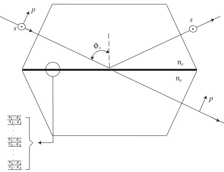
3.2 Periodic multilayer stacks
φ
οn
0n
0p
s
p
s
n 2 , d 2 n 1 , d 1
. . .
. . n 2 , d 2 n1 , d 1
.
n 2 , d 2 n 1 , d 1
The multilayer PBS, Fig. 4, consists of periodically repeated low-index (n1) – high-index
(n2) bilayers embedded in a high-index prism of refractive index n0. All media are considered to
be transparent, optically isotropic, and separated by parallel-plane boundaries. We assume that n0
> n1, n2 ≥ n0 and that light is incident from medium 0 at an angle of φ0 which is greater than the
critical angle [φc01 = arcsin(n1/n0)] of the 01 interface, so that frustrated total internal reflection
takes place.
Consider a monochromatic light beam traveling in an ambient medium (high-index prism) of refractive index n0 and incident on an embedded periodic multilayer structure at an
angle of incidence φ0 with respect to the normal to the interfaces, as shown in Fig. 4. The
complex-amplitude transmission and reflection coefficients andTν Rν (ν = p,s) of the multilayer
stack for the p and s polarizations at an internal angle of incidence φ0 are determined by the scattering matrix method16. A general expression for the complex-amplitude reflection coefficient (Rν) for an m-layer periodic multilayer stack with a bilayer as a period embedded in a
high-index prism, as shown in Fig. 4, can be expressed as:
. ,
, ... ...
0 1
2 1 2
0 1
2 1 2
s p
b X
b X b
a X
a X a
R n
n n n
n n n n
=
+ + +
+ + +
= −
− − −
ν
ν (15)
In Eq. (15) n = m/2, and an, an-1,… a0; bn, bn-1, … b0 are functions of the Fresnel interface
reflection and transmission coefficients r01ν, r12ν,r20νand X1. X1 and X2 are complex exponential
),Xi =exp(−jπZi cosφi (16) where Zi is the thickness of the ith film normalized to the quarter-wave thickness at normal
incidence, i.e,
. 4
λi i
i
n d
Z = (17)
In Eq. (16) φi is the angle of refraction in the ith layer, and in Eq. (17) ni, di are the refractive
index and metric thickness of the ith layer, respectively, and λ is the vacuum wavelength of light. The Fresnel complex-amplitude reflection and transmission coefficients of the ij interface for the
p and s polarizations are given by16:
j i i j j i i j ijp n n n n r φ φ φ φ cos cos cos cos + − = , j j i i j j i i ijs n n n n r φ φ φ φ cos cos cos cos + −
= (18)
j i i j i i ijp n n n t φ φ φ cos cos cos 2 + = , . cos cos cos 2 j j i i i i ijs n n n t φ φ φ +
= (19)
To suppress the ν polarization on reflection, we set Rν =0in Eq. (15) which gives
= 0. (20)
0 1
2 1
2 a X ... a
X
a n
n n
n + + +
− −
Depending on the order n of the polynomial in Eq. (20) multiple roots for X2 are obtained for
designs with number of layers m > 2, corresponding to multiple solutions sets (X1, X2) that
When the refractive indices and angle of incidence are such that n1/n0< , FTIR takes
place at the 01 interface at and the light field becomes evanescent in medium 1 (the low-index
film). In this case,
0 sinφ
0 φ
1
cosφ is pure imaginary, and X1 is real in the range 0 ≤ X1 ≤ 1. Because we
also choose n2 ≥ n0, the angle of refraction φ2 in the high-index layers is real, which makes X2 a
pure phase factor, so that |X2| = 1. For each real value of X1in the range 0 ≤ X1 1, we find
that |X
≤
2| = 1 for (n-1) roots of Eq. (20). Therefore, there are infinite number of solution sets (X1,
X2) that satisfy Eq. (20), so that Rν = 0. The corresponding solution sets of normalized film
thicknesses (Z1, Z2) are determined subsequently using Eq. (17).
An acceptable design must have a high reflectance | |2
' ν
ν R
R = for the unsuppressed
orthogonal polarization ν'. In general, this reflectance increases as the normalized thickness Z
1
(of the low-index layers that support the evanescent field) and the angle of incidence are
increased.
0 φ
4. Results
4.1 Centro-symmetric multilayer stacks as PBS
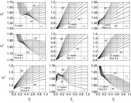
Various multilayer designs obtained by solving Eq. (5), their angular and spectral sensitivities are presented here. Figures 5, 6 and 7 show Z2 versus Z1 such that Rp = 0 at angles of
incidence φ0 from 45o to 55o in steps of 1o for various centro-symmetric multilayer stacks with 3, 7, 11, 15 and 19 layers of BaF2 and PbTe thin films embedded in a Cleartran36 (ZnS) prism.
1.45 1.50 1.55 1.60 1.65 1.70 0.7 0.8 0.9 1.0 1.1 1.2 1.36 1.40 1.44 1.48 1.52 1.56 1.70 1.75 1.80 1.85 1.90 0.4 0.5 0.6 0.7 0.8 0.9 1.0 0.8 0.9 1.0 1.1 1.2 1.3 1.4
0.0 0.2 0.4 0.6 0.8 1.0 1.2
1.3 1.4 1.5 1.6
0.0 0.2 0.4 0.6 0.8 1.0 1.60
1.64 1.68 1.72 1.76
0.0 0.2 0.4 0.6 0.8 1.0 1.80 1.85 1.90 1.95 2.00 Z 2 A 1 C 3 Layers 45o 55o B 1 7 Layers Root # 1
45o
55o
B 2 7 Layers
Root # 2 45
o 55o Z 2 B 3 C 7 Layers Root # 3
45o
55o
C 1 11 Layers Root # 1
45o
55o
C 2 11 Layers Root # 2
45o 55o Z 2 Z1 C 3 11 Layers
Root # 3
45o
55o
Z1
C 4 11 Layers
Root # 4
45o 55o Z1 C 5 C 11 Layers
Root # 5 45o
55o
Figure 5 Z2 versus Z1 such that Rp = 0 at angles of incidence φ0 from 45o to 55o in steps of 1o for centro-symmetric
multilayer stacks with BaF2 and PbTe thin films embedded in a ZnS substrate with refractive indices n0 = 2.1919
(ZnS), n1 = 1.3926 (BaF2), and n2 = 5.6314 (PbTe) in the IR at λ= 10.6 μm. Panel A1 corresponds to a trilayer
The refractive indices of ZnS (n0 = 2.1919), BaF2 (n1 = 1.3926), and PbTe (n2 = 5.6314) are
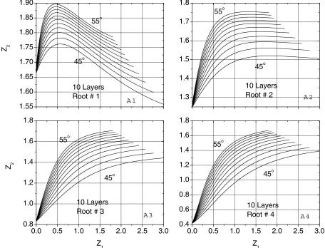
calculated using published dispersion relations.37 In Fig. 5, Panel A1 corresponds to the trilayer design with one root; Panels B1, B2 and B3 correspond to the 7-layer design with 3 roots, while Panels C1, C2, C3, C4 and C5 correspond to the 11-layer design with 5 roots.
0.2 0.4 0.6 0.8 1.0 1.2 0.6 0.8 1.0 1.2 1.4 0.9 1.0 1.1 1.2 1.3 1.4 1.2 1.3 1.4 1.5 1.6
0.0 0.2 0.4 0.6 0.8 1.0 1.48 1.52 1.56 1.60 1.64 1.68
0.0 0.2 0.4 0.6 0.8 1.0 1.85
1.90 1.95 2.00 2.05
0.0 0.2 0.4 0.6 0.8 1.0 1.72 1.76 1.80 1.84 Z 2 A 1 15 Layer Root # 1
45o 55o
A 2
15 Layer Root # 2
45o 55o
A 3
15 Layer Root # 3
45o 55o
Z 2
A 4
15 Layer Root # 4
45o 55o
Z1
A 5
15 Layer Root # 5
45o 55o Z1 A 6 C 15 Layer Root # 6
45o 55o Z 2 Z1 A 7 15 Layer Root # 7 45o 55o
Figure 6Z2 versus Z1 such that Rp = 0 at angles of incidence φ0 from 45o to 55o in steps of 1o for the same material
system as described in the caption of Fig. 5 for a 15-layer centro-symmetric design.
represents a thickness solution that achieves a polarizer (Rp = 0) at the angle of incidence marked
by that curve.
0.2 0.4 0.6 0.8 1.0 1.2 0.4 0.6 0.8 1.0 1.2 1.4 0.7 0.8 0.9 1.0 1.1 1.2 0.9 1.0 1.1 1.2 1.3 1.4 1.15 1.20 1.25 1.30 1.35 1.40 1.45 1.35 1.40 1.45 1.50 1.55 1.60 1.65
0.0 0.2 0.4 0.6 0.8 1.0 1.85
1.90 1.95 2.00 2.05
0.0 0.2 0.4 0.6 0.8 1.0 1.60 1.64 1.68 1.72 1.76 1.80
0.0 0.2 0.4 0.6 0.8 1.0 1.75 1.80 1.85 1.90 Z 2 A 1 19 Layers Root # 1
45o 55o
A 2
19 Layers Root # 2
45o 55o
A 3
19 Layers Root # 3
45o 55o
Z 2
A 4
19 Layers Root # 4
45o 55o
A 5
19 Layers Root # 5
45o 55o
A 6
19 Layers Root # 6
45o 55o Z 2 Z1 A 7 19 Layers Root # 7
45o 55o
Z1
A 8
19 Layers Root # 8
45o 55o
Z1 A 9
19 Layers Root # 9
C
45o
55o
Figure 7 Z2 versus Z1 such that Rp = 0 at angles of incidence φ0 from 45o to 55o in steps of 1o for the same material
system as described in the caption of Fig. 5 for a 19-layer centro-symmetric design.
For designs with 3 to 19 layers, the Z2-vs-Z1 curves that correspond to some roots are clustered
and mutually intersecting in a small region of the Z2-vs-Z1 plane. By selecting an intersection
point (Z1, Z2) of two curves in this cluster we obtain an Rp = 0 polarizer at two angles of
each design with 3 to 19 layers, the intersection point of the 50o and 55o curves that correspond to the root with the highest root number (Panel A1 of Fig. 5, Panel B3 of Fig. 5, Panel C5 of Fig. 5, Panel A7 of Fig. 6, and Panel A9 of Fig. 7 for the 3, 7, 11, 15 and 19-layer designs, respectively). The point of intersection of the 50o and 55o curves for the root with the highest root number yields a design with Rp ≈ 0 and high reflectance |Rs|2 for all angles of incidence
from 45o to 55o. Figures 5-7 are magnified so that the details are more apparent. Table 2 lists the normalized and metric film thicknesses (Z1, Z2) and (d1, d2) obtained by the above procedure for
the 3, 7, 11, 15 and 19-layer designs.
Table 2 Normalized (Z1, Z2) and metric (d1, d2) thicknesses corresponding to the point of intersection of the 50o and
55oZ2-vs-Z
1 curves in Panel A1 of Fig 5, Panel B3 of Fig. 5, Panel C5 of Figure 5, Panel A7 of Fig. 6, and Panel A9
of Fig. 7 for the 3, 7, 11, 15 and 19-layer designs, respectively.
# of Layers Z1 Z2 d1 (μm) d2 (μm)
3 0.377275 1.588134 0.71792 0.74734
7 0.234571 1.840903 0.44637 0.86628
11 0.188795 1.701440 0.35926 0.80066
15 0.173570 1.807341 0.33029 0.85049
19 0.149774 1.866958 0.28501 0.87855
4.1.1 Angular sensitivity
This specific comparison between different multilayer designs is based on the thickness solutions (Z1, Z2) ↔ (d1, d2) listed in Table 2. For the angle sensitivity, the metric film
thicknesses (d1, d2) and wavelength λ = 10.6 μm for each multilayer design are kept constant and
the angle of incidence φ0 is varied from 46o to 56o. Panels A1 and A2 of Fig. 8 show a
comparison between the extinction ratios in reflection and transmission (ERr and ERt in dB),
respectively, as a function of angle of incidence φo for the 3, 7, 11, 15 and 19-layer designs. The 15- and the 19-layer designs achieve ERr and ERt > 30 dB over a 10o internal field of view (from
46
47
48
49
50
51
52
53
54
55
56
6
12
18
24
30
36
30
60
90
120
150
180
ER
t
(d
B)
Angle of Incidence
φ0(deg)
3
7
11
15
19
A 2
ER
r
(d
B)
3
7
11
15
19
11
15
19
7
3
A 1
Figure 8 Extinction ratios in reflection and transmission (ERr and ERt) in dB for various centro-symmetric
multilayer stacks with 3-19 layers embedded in a ZnS substrate are plotted versus the angle of incidence φ0 from 46o to 56o. The material system is the same as given in the caption of Fig. 5 and the metric film thicknesses
If one accounts for the refraction of light from air to the high-index ZnS substrate, the angular bandwidth in air is more than double that indicated in Fig. 8. The extinction ratio ERr is > 150
dB at 50o and 55o for all designs because each thickness solution set corresponds to (Z1 ,Z2) at the
point of intersection of the 50o and 55o curves. Table 3 lists the discrete angles at which ERr in
Panel A1 of Fig. 8 reaches a peak.
Table 3 Discrete angles at which the extinction ratio in reflection (ERr) reaches a peak in Panel A1 of Fig. 8.
# of Layers φ0 (deg) ERr (dB) ERt (dB)
50o 162 8.9
3
55o 168 10
50o 168 15.4
7
55o 168 16.9
50o 180 25.4
51.63o 114 25.8
11
55o 170 26.6
46.97o 92 30.6
50o 173 31.5
15
55o 171 33.1
50o 161 34.4
19
55o 159 36.2
Panels A1, A2, A3, A4 and A5 of Fig. 9 show the intensity reflectances |Rp|2and |Rs|2 as
a function of the angle of incidence φ0 from 46o to 56o for 3-, 7-, 11-, 15- and 19-layer designs, respectively. All the parameters in this plot correspond to those in Fig. 8. As the number of layers increase, |Rs|2 increases from 84% to 99.98% while |Rp|2remains < 0.01 over a 10o internal
field of view (46o to 56o). The 15-layer design achieves |R
p|2 < 0.00025 and |Rs|2 > 0.999 while
the 19-layer design achieves |Rp|2 < 0.0005 and |Rs|2 > 0.9995 over a 10o field of view (from 46o
0.0 2.0x10⁻³
4.0x10⁻³
6.0x10⁻³
|Rp|2 |Rs|2
3 Layers A 1 0.84 0.85 0.86 0.87 0.88 0.89 0.90 0.91 0.0 3.0x10⁻³ 6.0x10⁻³ 9.0x10⁻³ 1.2x10⁻²
|Rp|2 |Rs|2
7 Layers A 2 0.960 0.965 0.970 0.975 0.980 0.985 0.0 5.0x10⁻⁴ 1.0x10⁻³ 1.5x10⁻³ 2.0x10⁻³
|Rp|2 |Rs|2
11 Layers A 3 0.9964 0.9966 0.9968 0.9970 0.9972 0.9974 0.9976 0.9978 0.9980
46 47 48 49 50 51 52 53 54 55 56 0.0 5.0x10⁻⁵ 1.0x10⁻⁴ 1.5x10⁻⁴ 2.0x10⁻⁴ 2.5x10⁻⁴
Angle of Incidence φ0 (deg) |Rp|2
|Rs|2
15 Layers A 4 0.9990 0.9991 0.9992 0.9993 0.9994 0.9995 0.9996
46 47 48 49 50 51 52 53 54 55 56 0.0 1.0x10⁻⁴ 2.0x10⁻⁴ 3.0x10⁻⁴ 4.0x10⁻⁴ 5.0x10⁻⁴
Angle of Incidence φ0 (deg) |Rp|2
|Rs|2
19 Layers A 5 0.99950 0.99955 0.99960 0.99965 0.99970 0.99975 0.99980
|Rp|2
|Rs|2
Figure 9 Reflectances |Rp|2 and |Rs|2 for various centro-symmetric multilayer stacks with 3-19 layers embedded in a
ZnS substrate are plotted versus the angle of incidence φ0 from 46o to 56o.The material system is the same as given
in the caption of Fig. 5 and the metric film thicknesses associated with different multilayer stack designs are listed in Table 2.
4.1.2 Spectral sensitivity
The spectral sensitivities of the multilayer designs obtained in Section 4.1.1 are now analyzed. For the spectral sensitivity, the metric film thicknesses (d1, d2) and the angle of
0 20 40 60 80
ERr (dB) ERt (dB) ERr ERt 3 Layers A 1 -2 0 2 4 6 8 10 -60 -40 -20 0 20 40 60 80 ERr ERt 7 Layers A 2 -15 -10 -5 0 5 10 15 20 -40 -20 0 20 40 60 80 ERr ERt 11 Layers A 3 -20 -10 0 10 20 30
8 9 10 11 12
-60 -40 -20 0 20 40 60 80
Wavelength λ (μm) ERr ERt 15 Layers A 4 -20 -10 0 10 20 30 40
8 9 10 11 12
-60 -40 -20 0 20 40 60 80
Wavelength λ (μm) ERr ERt 19 Layers A 5 -20 -10 0 10 20 30 40
Figure 10 Extinction ratios in reflection and transmission (ERr and ERt) in dB for various centro-symmetric
multilayer stacks with 3-19 layers embedded in a ZnS substrate are plotted versus wavelength 8≤λ ≤12 μm. The material system is the same as given in the caption of Fig. 5 and the metric film thicknesses associated with different multilayer stack designs are listed in Table 2.
All parameters for each panel in Fig. 10 are the same as those in Fig. 9. All the designs with 3-19 layers have a peak in ERr at λ = 10.6 μm, which is the design wavelength. These
devices also function as Rp = 0 polarizers, at additional discrete wavelengths other than the
design wavelength. An interesting feature of these plots in Fig. 10 is that designs with a higher number of layers (>3) function as orthogonal polarizers (Rs = 0) or PBS at other discrete
Table 4 Discrete wavelengths at which the extinction ratio in reflection (ERr) of Fig. 10 reaches a positive or
negative peak.
# of Layers λ (μm) ERr (dB) ERt (dB)
3 10.6 82.43 8.95 8.862 -66.08 -8.21 7
10.6 77.05 15.44 8.318 -60.53 -11.87 9.477 69.06 22.05 11
10.6 81.08 25.48 8.582 -57.91 -17.72 8.886 -53.9 -14.48
9.85 63.92 26.44 15
10.6 77.62 31.55 8.486 -53.73 -19.94 8.991 -57.91 -18.51 9.22 -55.02 -15.44 10.032 64.28 28.48
10.6 75.73 34.46 19
11.652 80.66 31.92
Panels A1, A2, A3, A4 and A5 of Fig. 11 show the intensity reflectances |Rp|2and |Rs|2 as
a function of wavelength λ from 8 to 12 μm for 3-, 7-, 11-, 15- and 19-layer designs, respectively. All parameters for each panel in Fig. 11 are the same as those in Fig. 10. The |Rp|2
curves of all the designs with 3-19 layers dip to zero at λ = 10.6 μm, which is the design wavelength. The 11-, 15- and 19-layer designs function as effective s-reflection polarizers with s
reflectance |Rs|2 > 99% over a 2 to 3 μm spectral bandwidth. The associated p reflectance is not
low enough in these spectral regions to qualify these devices for polarizing beam splitters. The 19-layer design functions as an effective s-reflection polarizer with |Rs|2 > 99% over 9.5<λ<12 μm and also as a p-reflection polarizer with |Rp|2 > 99% over 8.2<λ<9 μm. With an increase
0.0 0.1 0.2 0.3 0.4 0.5 0.6 0.7
|Rp|2
|Rs|2 |Rp|2
|Rs|2
3 Layers A 1 0.60 0.65 0.70 0.75 0.80 0.85 0.90 0.0 0.2 0.4 0.6 0.8 1.0
|Rp|2 |Rs|2
7 Layers A 2 0.0 0.2 0.4 0.6 0.8 1.0 0.0 0.2 0.4 0.6 0.8 1.0
|Rp|2 |Rs|2
11 Layers A 3 0.0 0.2 0.4 0.6 0.8 1.0
8 9 10 11 12
0.0 0.2 0.4 0.6 0.8 1.0
Wavelength λ (μm) |Rp|2 |Rs|2
15 Layers A 4 0.0 0.2 0.4 0.6 0.8 1.0
8 9 10 11 12
0.0 0.2 0.4 0.6 0.8 1.0
Wavelength λ (μm) |Rp|2
|Rs|2
19 Layers A 5 0.0 0.2 0.4 0.6 0.8 1.0
Figure 11 Reflectances |Rp|2 and |Rs|2 for various centro-symmetric multilayer stacks with 3-19 layers embedded in a
ZnS substrate are plotted versus wavelength 8≤λ ≤12 μm. The material system is the same as given in the caption of Fig. 5 and the metric film thicknesses associated with different multilayer stack designs are listed in Table 2.
4.2 Centro-symmetric multilayer stacks as complete transmission QWR and
HWR devices
4.2.1 IR QWR device using an embedded SiO2-Si multilayer stack in GaP prism
A specific QWR cube design (φ0 =45o)at the lightwave-communications wavelength of λ = 1.55 μm uses a centro-symmetric 11-layer stack of Si (n0 = 3.4777) and SiO2 (n1 = 1.4444)
thin films embedded in a high-index GaP (n2 = 3.0535) prism. The angle of incidence φ0 = 45o is
above the critical angle of the 0-1 interfaceφcrit = 28.23o, so that FTIR takes place. With the
design parameters listed in Table 5 we calculate Tp 2 = Ts 2 =0.999999 and Δt= 90.0005o.
0.9975 0.9980 0.9985 0.9990 0.9995 1.0000
0.994 0.995 0.996 0.997 0.998 0.999 1.000
1.50 1.51 1.52 1.53 1.54 1.55 1.56 1.57 1.58 1.59 1.60 87
88 89 90 91 92 93
44.0 44.2 44.4 44.6 44.8 45.0 45.2 45.4 45.6 45.8 46.0 84
86 88 90 92 94 96 98
Int
ensi
ty Tr
ansmi
ttance T
A 1 B 1
A 2 B 2
Phase Ret
ar
dat
ion
Δt
(
deg)
Wavelength λ (μm) Angle of Incidence Φ0 (deg) |Ts|2
|Tp|2
|Ts|2
|Tp|2
Figure 12 Panels (A1, A2) and (B1, B2) show the spectral and angular sensitivities, respectively, of a QWR cube design that operates at λ=1.55 μm and φ0 = 45o. The design uses an 11-layer stack of Si (n0 = 3.4777) and SiO2 (n1
= 1.4444) thin films embedded in a high-index GaP (n2 = 3.0535) prism. The thicknesses of the SiO2 and Si thin
films are 17.5 nm and 67.1 nm, respectively. Both the p and s transmittances |Tp|2 and |Ts|2 and the differential
transmission phase shiftΔtare represented in this figure.
Table 5 Normalized (Z1, Z2) and metric (d1, d2) thicknesses corresponding to the complete transmission QWR and HWR devices presented in Section 4.2
Device Z1 Z2 d1 (nm) d2 (nm)
QWR 0.065103 0.601902 17.5 67.1
HWR 0.164135 2.001336 44.0 223.0
It is of interest to consider the spectral and angular sensitivities of the above QWR design. For the spectral sensitivity, the film thicknesses d1 = 17.5 nm, d2 = 67.1 nm and the angle
of incidence φ0= 45o are kept constant, and the wavelengthλ is scanned over a 100-nm range from 1.5 to 1.6 μm.The dispersion of all materials in this spectral region is accounted for.37,38
For the angle sensitivity, the film thicknesses d1 = 17.5 nm, d2 = 67.1 nm and the wavelength
m
μ
λ=1.55 are kept constant, and the internal angle of incidence φ0is varied by 1± o.
Panel A1 of Fig. 12 shows that |Tp|2 and |Ts|2 remain > 99.75 % over the 100-nm spectral
region with a locally flat maximum (100 % transmission) at the design wavelength λ = 1.55μm, hence the amplitude diattenuation in transmission is < 0.2 %. Panel A2 of Fig. 12 shows that the differential phase shift Δtdeviates from 90o by < ±3o over the 100-nm spectral range. Panels
B1 and B2 of Fig. 12 show |Tp|2, |Ts|2 and Δt as functions of the angle of incidenceφ0. |Tp|
2 and
|Ts|2 remain high (> 99.4%) while Δtdeviates from 90o by <±7o for ±1o change in the internal
angle of incidence around φ0 =45o. The field of view in air is larger than that in prism by a factor of 3.
We now consider the sensitivity of this QWR to film-thickness errors by keeping the wavelength λ=1.55μm and angle of incidence φ0 =45o constant, and varying the thickness di of
the ith film (i = 1, 2, …., 11) by 5 % around its design value. (The films are numbered starting from the medium of incidence.) The resulting small shifts in the transmittances |T
±
p|2 and |Ts|2
Fig. 13. The left Panels A1, A2, and A3 of Fig. 13 show the effect of thickness errors of the odd-numbered low-index (SiO2) films, whereas the right Panels B1, B2, and B3 show the effect of
errors in thickness of the even-numbered high-index (Si) films. Because of the symmetry of the design stack, thickness errors for films that are symmetrically located above and below the center layer (e.g., 1 and 11, 2 and 10, and 3 and 9) produce identical shifts in the retarder’s response. The effect of simultaneous errors in the thicknesses of all films can be determined, to first order in retardance or second order in transmittances, by superposition of the results shown in Fig. 13.
0.9995 0.9996 0.9997 0.9998 0.9999 1.0000 0.9987 0.9990 0.9993 0.9996 0.9999 0.99994 0.99996 0.99998 1.00000 0.99980 0.99985 0.99990 0.99995 1.00000
-5 -4 -3 -2 -1 0 1 2 3 4 5 88.5 89.0 89.5 90.0 90.5 91.0 91.5
-5 -4 -3 -2 -1 0 1 2 3 4 5 89.1 89.4 89.7 90.0 90.3 90.6 90.9 Transmittance |T p | 2 A 1 1,11 3,9 5,7 B 1 2,10 4,8 6 Transmittance |T s | 2 A 2 3,9 1,11 5,7 B 2 6 4,8 2,10 Phase Retardation Δt (deg)
% Error in di A 3
1,11 3,9
5,7
% Error in di B 3
6 4,8
2,10
Figure 13 Panels (A1, A2, A3) and (B1, B2, B3) show the sensitivities of the QWR cube design that operates at λ = 1.55 μm andφ0 = 45o to errors of thickness of the odd- and even-numbered films, respectively. Both the p and s
transmittances |Tp|2 and |Ts|2 and the differential transmission phase shift t
Δ are represented in this figure. The design uses an 11-layer stack of Si (n0 = 3.4777) and SiO2 (n1 = 1.4444) thin films embedded in a high-index GaP (n2 =
3.0535) prism. The thicknesses of the SiO2 and Si thin films are changed by ±5 % around the design values of 17.5
4.2.2 IR HWR device using an embedded SiO2-Si multilayer stack in Si prism
An HWR cube design atλ = 1.55 μm uses a centro-symmetric 7-layer stack of Si (n2 =
3.4777) and SiO2 (n1 = 1.4444) thin films embedded in a high-index Si (n0 = 3.4777) prism. The
angle of incidence ( 0 45 )is above the critical angle of the 0-1 interface (
o =
φ φcrit =24.54o),
hence FTIR takes place. With the design parameters listed in Table 5 we calculate
999999 .
0 2 2
=
= s
p T
T and Δt= 179.98o.
0.91 0.92 0.93 0.94 0.95 0.96 0.97 0.98 0.99 1.00
0.86 0.88 0.90 0.92 0.94 0.96 0.98 1.00
1.50 1.51 1.52 1.53 1.54 1.55 1.56 1.57 1.58 1.59 1.60 179.85
179.90 179.95 180.00 180.05 180.10 180.15 180.20 180.25 180.30
44.0 44.2 44.4 44.6 44.8 45.0 45.2 45.4 45.6 45.8 46.0 165
170 175 180 185 190 195
|Ts|2
|Tp|2 |Ts|2
|Tp|2
A 1 B 1
Wavelength λ (μm)
Phase Ret
ar
dat
ion
Δt
(
deg)
Int
ensi
ty Tr
ansmi
ttance T
Angle of Incidence Φ0 (deg)
A 2 B 2
Figure 14 Panels (A1, A2) and (B1, B2) show the spectral and angular sensitivities, respectively, for an HWR cube design that operates at λ = 1.55 μm and φ0 = 45o that uses a centro-symmetric 7-layer stack of Si (n2 = 3.4777) and
SiO2 (n1 = 1.4444) thin films embedded in a Si prism (n0 = 3.4777). The design thicknesses of the SiO2 and Si thin
films are d1 =44.0 nm and d2 = 223.0 nm, respectively. Both the p and s transmittances |Tp|2 and |Ts|2 and the
Figure 14 shows the spectral and angular sensitivities of the HWR design. The dispersion of Si and SiO2 in the 100-nm spectral region is accounted for.37,38 Panel A1 of Fig. 14 shows that
|Tp|2 and |Ts|2 remain > 91 % over the 100-nm spectral region with a locally flat maximum (= 100
%) at the design wavelength λ = 1.55μm. The amplitude diattenuation is < 3 %. Panel A2 of Fig. 14 shows thatΔtdeviates from 180o by ≤ ±0.3o over the 100-nm spectral range. Panels B1
and B2 of Fig. 14 show |Tp|2, |Ts|2 and Δt as functions ofφ0. |Ts|
2 remains high (> 98 %), whereas
|Tp|2 dips to 87.5 %, as the angle of incidence is changed by ±1o. The differential transmission
phase shift Δtdeviates from 180o by < ±17o (< 10 %) for ±1o change in the internal angle of
incidence around φ0 =45o. The field of view of the HWR in air is wider (by a factor n0 > 3), if
one accounts for light refraction from air to Si at the entrance face of the prism.
The sensitivity of this HWR design to film-thickness errors is considered by holding the wavelength λ=1.55μm and angle of incidence φ0 =45o constant, and by varying each film thickness di (i = 1, 2, …., 7) by 5 % around its design values. The resulting shifts in the
transmittances |T
±
p|2 and |Ts|2 (which are parabolic) are represented by Panels A1 and B1 of Fig.
15, and the corresponding shifts in the differential phase shift Δt(which are linear) are shown in
0.9980 0.9985 0.9990 0.9995 1.0000
0.93 0.94 0.95 0.96 0.97 0.98 0.99 1.00
-5 -4 -3 -2 -1 0 1 2 3 4 5 176
178 180 182 184
-5 -4 -3 -2 -1 0 1 2 3 4 5 172
174 176 178 180 182 184 186 188
Int
ensi
ty Tr
ansmi
ttance T
|Tp|2
|Ts|2 1,3,5,7
1,7
3,5
A 1
|Tp|2 |Ts|2 2,6
4
4 2,6
B 1
Phase Ret
ar
dat
ion
Δt
(
deg)
% Error in di
1,7 3,5
A 2
% Error in di
2,6
4
B 2
Figure 15 Transmittances |Tp|2 and |Ts|2 for p- and s-polarized light and differential transmission phase shift t
Δ of an HWR cube design, that operates at λ = 1.55 μm and φ0 = 45o, are plotted versus the error of thickness of each film.
The design uses a 7-layer stack of Si (n0 = 3.4777) and SiO2 (n1 = 1.4444) thin films embedded in a high-index Si
(n2 = 3.4777) prism. The thicknesses of the SiO2 and Si thin films are changed by ±5 % around the design values of
44.0 nm and 223.0 nm, respectively.
4.3 Centro-symmetric multilayer stacks as 50%-50% beam splitters
Table 6 50%-50% beam splitter cube designs in the visible, near-infrared and CO2 laser wavelength
# of
Layers n0 n1 n2 |Rp|2 |Rs|2 Δr Δt Z1 Z2
|Rp|2 = |Rs|2 = |Tp|2 = |Ts|2 ≈ 0.5; r
Δ = 0o and t
Δ =0o; λ= 10.6 μm;
0
φ =45o
15 3.2919 1.5251 5.6315 0.49908 0.49908 0 -0.01176 0.223961 1.120375
15 2.6817 1.2975 3.2919 0.499341 0.499341 0 -0.00844 0.354839 1.251386
19 2.1919 1.3765 4.0038 0.498492 0.498492 0 -0.00857 0.704937 0.809739
|Rp|2 = |Rs|2 = |Tp|2 = |Ts|2 ≈ 0.5; r
Δ = 0o and t
Δ =180o; λ= 10.6 μm;
0
φ =45o
3 4.0038 1.2975 4.0038 0.501783 0.501783 0 -180.027 0.161472 2.307135
15 3.4177 1.2289 3.4177 0.498157 0.498157 0 -180.013 0.060328 2.605541
15 2.1919 1.2853 2.6705 0.499078 0.499078 0 -180.011 0.628729 1.135609
19 4.0038 1.2975 5.6315 0.499729 0.499729 0 -180.107 0.096582 1.517991
19 2.4026 1.5251 4.0038 0.500165 0.500165 0 -179.992 0.766485 0.774465
|Rp|2 = |Rs|2 = |Tp|2 = |Ts|2 ≈ 0.5; r
Δ =180o and t
Δ =0o; λ= 10.6 μm;
0
φ =45o
15 2.4026 1.2289 5.6315 0.49908 0.49908 180 0.014662 0.113143 0.765634
|Rp|2 = |Rs|2 = |Tp|2 = |Ts|2 0.5;≈ r
Δ =180o and t
Δ =180o; λ= 10.6 μm;
0
φ =45o
19 2.1919 1.3765 5.6315 0.499115 0.499115 -180 -180.056 0.441946 0.549033
15 2.1919 1.2975 5.6315 0.499757 0.499757 180 179.8184 0.364796 0.887992
19 2.1919 1.3765 5.6315 0.499115 0.499115 -180 -180.056 0.441946 0.549033
|Rp|2 = |Rs|2 = |Tp|2 = |Ts|2 ≈ 0.5; r
Δ = 0o and t
Δ =0o; λ= 1.55 μm;
0
φ =45o
15 2.2710 1.3827 2.7332 0.501649 0.501649 0 -0.00051 0.883346 1.143537 15 2.2710 1.3193 2.4555 0.501745 0.501745 0 -0.02347 0.84304 1.128708
|Rp|2 = |Rs|2 = |Tp|2 = |Ts|2 ≈ 0.5; r
Δ = 0o and t
Δ =180o; λ= 1.55 μm;
0
φ =45o
15 2.7332 1.3568 3.0535 0.501154 0.501154 0 180.0194 0.447349 1.406845 15 2.4555 1.3827 3.0535 0.501635 0.501635 0 -179.996 0.518109 1.177792
|Rp|2 = |Rs|2 = |Tp|2 = |Ts|2 ≈ 0.5; r
Δ = 0o and t
Δ =0o; λ= 0.633 μm;
0
φ =45o
15 2.5283 1.4732 2.7276 0.499148 0.499148 0 -0.0207 0.857317 1.125254 19 2.7276 1.4732 2.9886 0.498596 0.498596 0 0.015666 0.535905 1.488865
|Rp|2 = |Rs|2 = |Tp|2 = |Ts|2 0.5;≈ r
Δ = 0o and t
Δ =180o; λ= 0.633 μm;
0
φ =45o
Table 6 continued…
|Rp|2 = |Rs|2 = |Tp|2 = |Ts|2 ≈ 0.5; r
Δ =-90o and t
Δ =90o; λ= 10.6 μm;
0
φ =45o
7 3.2919 1.2289 4.0038 0.499805 0.499805 -90 89.91616 0.192835 1.65936 7 2.4026 1.2853 2.6817 0.501552 0.501552 -90 90.06921 0.634811 1.372146 7 2.1919 1.2975 2.402 0.500867 0.500867 -90 90.09664 0.979812 1.184854 11 2.1919 1.2975 5.6315 0.500025 0.500025 -90 90.0197 0.297014 0.933023 11 2.6705 1.6247 4.0038 0.50001 0.50001 -90 90.01103 0.599676 0.705015 15 2.6817 1.5845 3.4177 0.500747 0.500747 -90 90.15455 0.726915 1.177706 15 2.6817 1.2853 3.4177 0.500643 0.500643 -90 90.18617 0.334382 1.213735 15 2.4026 1.4540 3.4177 0.501643 0.501643 -90 90.29479 0.704173 1.052177 19 4.0038 1.5251 5.6315 0.498192 0.498192 -90 89.97159 0.137287 1.441707 19 3.4177 1.5251 5.6315 0.499186 0.499186 -90 89.97817 0.17862 1.115979
|Rp|2 = |Rs|2 = |Tp|2 = |Ts|2 ≈ 0.5; r
Δ =-90o and t
Δ =90o; λ= 1.55μm;
0
φ =45o
7 3.0535 1.4660 3.4777 0.500666 0.500666 -90 90.06338 0.430118 1.50383 7 2.7332 1.4660 3.0535 0.501409 0.501409 -90 89.92518 0.640199 1.366176 7 2.4555 1.4260 3.4777 0.499162 0.499162 -90 90.02917 0.518429 1.004559 7 2.2710 1.3827 3.4777 0.500523 0.500523 -90 89.94589 0.588979 0.697851 15 2.4555 1.3827 3.0535 0.501418 0.501418 -90 89.83067 0.622599 1.296565 15 2.2710 1.3827 3.0535 0.500372 0.500372 -90 90.13153 0.773497 1.07054
|Rp|2 = |Rs|2 = |Tp|2 = |Ts|2 ≈ 0.5; r
Δ =-90o and t
Δ =90o; λ= 0.633μm;
0
φ =45o
15 2.6398 1.4880 2.9886 0.500048 0.500048 -90 90.1086 0.736006 1.255242 15 2.5906 1.4576 2.9886 0.499266 0.499266 -90 90.176 0.684477 1.096744 15 2.5728 1.4328 2.9886 0.499512 0.499512 -90 90.10218 0.649959 1.106903 15 2.5283 1.3615 2.9886 0.49854 0.49854 -90 90.14496 0.555528 1.141683
|Rp|2 = |Rs|2 = |Tp|2 = |Ts|2 ≈ 0.5; r
Δ =-90o and t
Δ =-90o; λ=10.6μm;
0
φ =45o
7 2.6705 1.6247 4.0038 0.498731 0.498731 -90 -89.9782 0.562143 0.747104 11 3.4177 1.3765 4.0038 0.498686 0.498686 -90 -89.9887 0.247714 1.737035 19 3.2919 1.6247 5.6315 0.499703 0.499703 -90 -90.0106 0.267305 0.998882 19 2.4026 1.4540 5.6315 0.498884 0.498884 -90 -89.9687 0.307323 0.810862 19 2.6817 1.2289 4.0038 0.498217 0.498217 -90 -89.7005 0.236034 1.113749 19 2.6705 1.2289 4.0038 0.500829 0.500829 -90 -89.7088 0.238398 1.108369
|Rp|2 = |Rs|2 = |Tp|2 = |Ts|2 ≈ 0.5; r
Δ =-90o and t
Δ =-90o; λ=1.55μm;
0
φ =45o
7 2.2710 1.3568 3.4777 0.501304 0.501304 -90 -90.0069 0.503804 0.774306 15 2.4555 1.4443 2.5812 0.501941 0.501941 -90 -89.7613 1.070813 1.217802 19 2.5812 1.3827 3.4777 0.499941 0.499941 -90 -90.0069 0.461541 1.351135 19 2.4555 1.3193 3.4777 0.499728 0.499728 -90 -89.9778 0.440251 1.312026 19 2.2710 1.3568 2.5812 0.501898 0.501898 -90 -89.8111 0.899423 0.961746
|Rp|2 = |Rs|2 = |Tp|2 = |Ts|2 ≈ 0.5; r
Δ =-90o and t
Δ =-90o; λ=0.633μm;
0
φ =45o
4.3.1 50%-50% IR polarization-independent beam splitters (PIBS) using an embedded KBr-Ge multilayer stack in Si prism
A beam splitter that reflects and refracts light simultaneously without change of polarization is defined as a polarization independent beam splitter (PIBS). A specific PIBS design operating at the CO2 laser wavelength λ= 10.6 μ m and at an angle of incidence φ0= 60o
uses a centro-symmetric 15-layer stack of Ge (n0 = 4.0038) and KBr (n1 = 1.5251) thin films
embedded in a high-index Si (n2 = 3.4177) prism. The angle of incidence φ0 = 60o is above the
critical angle of the 0-1 interfaceφcrit= 26.50o, so that FTIR takes place. The solution sets for the normalized thicknesses are listed in Table 7.
Table 7 Normalized (Z1, Z2) thicknesses corresponding to the 50%-50% beam splitters presented in Sections 4.3.1, 4.3.2, 4.3.3 and 4.3.4
# of
Layers φ0 n0 n1 n2 |Rp|2 |Rs|2 Δr Δt Z1 Z2
15 60o 3.4177 1.5251 4.0038 0.498647 0.498647 0 -0.01 0.119278 2.277189
15 45o 3.4177 1.2289 3.4177 0.498157 0.498157 0 179.99 0.060328 2.605541
15 45o 2.4026 1.2289 5.6315 0.49908 0.49908 180 0.01 0.113143 0.765634
7 60o 2.1919 1.5251 5.6315 0.500553 0.500553 180 180.00 0.185617 0.591113
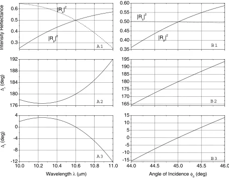
The spectral and angular sensitivities of the above PIBS design are considered now. For the spectral sensitivity, the film thicknesses d1 = 207.2 nm, d2 = 1507.2 nm and the angle of
incidence φ0= 60o are kept constant, and the wavelengthλ is scanned over a 100-nm range from 10 to 11μm. The dispersion of all materials in this spectral region is accounted for37. For the angle sensitivity, the film thicknesses d1 = 207.25 nm, d2 = 1507.2 nm and the wavelength
m
μ
λ=10.6 are kept constant, and the internal angle of incidence φ0is varied by ±1o.
Panel A1 of Fig. 16 shows that |Rp|2 and |Rs|2 vary from 0.0 to 0.65 over the 100-nm
shows that the differential phase shiftsΔr, Δtdeviate from 0o by < 14o over the 100-nm spectral
range. Panels B1 and B2 of Fig. 16 show |Rp|2, |Rs|2 Δrand Δt as functions of the angle of
incidenceφ0. |Rp|2 and |Rs|2 vary from 0.2 to 0.6 whileΔr, Δtdeviate from 0
o by < 17.5± o for ±1o
change in the internal angle of incidence around φ0 =60o.
0.0 0.1 0.2 0.3 0.4 0.5 0.6
0.2 0.3 0.4 0.5 0.6
10.0 10.2 10.4 10.6 10.8 11.0
0 3 6 9 12 15
59.0 59.5 60.0 60.5 61.0
-10 -5 0 5 10 15 20
In
tensi
ty Ref
lect
ance
A 1
|Rs|2 |Rp|2
B 1
|Rs|2
|Rp|2
P
hase Ret
ardat
ion (deg)
Wavelength λ (μm)
A 2
Δr , Δt
Angle of Incidence φ0 (deg)
B 2
Δr , Δt
Figure 16 Panels (A1, A2) and (B1, B2) show the spectral and angular sensitivities, respectively, of 50%-50% PIBS that operates at λ =10.6 μm and φ0 = 60o. The design uses a 15-layer stack of Ge (n0 = 4.0038) and KBr (n1 =
1.5251) thin films embedded in a high-index Si (n2 = 3.4177) prism. The thicknesses of the KBr and Ge thin films
are 207.2 nm and 1507.2 nm, respectively. Both the p and s reflectances |Rp|2 and |Rs|2 and the differential reflection