Ultra-Low Voltage Low Power Bulk Driven Z
Copy-Current Controlled-Current Differencing
Buffered Amplifier
Salma Bay Abo Dabbous and Ziad Alsibai
Dept. of Microelectronics, Brno University of Technology, Brno, Czech Republic Email: [email protected], [email protected]
Abstract—This paper presents Ultra Low Voltage (ULV)
Low Power (LP) Z Copy-Current Controlled-Current Differencing Buffered Amplifier (ZC-CC-CDBA) with single voltage supply. The circuit is performed using bulk driven (BD) technique and it is capable to operate at ULV of 0.65V and consumes low power in the micro range. In addition to the topology simplicity, the proposed circuit offers high linearity and extended output voltage range. Eventually, to verify the functionality of the proposed circuit, current mode multi-function biquad filter using three ZC-CC-CDBAs with two grounded capacitors is included as an example of application. The simulations are performed in PSPICE environment using the 0.18µm CMOS technology from TSMC.
Index Terms—bulk driven, current differencing buffered
amplifier, filter, low power circuit
I. INTRODUCTION
Minimizing the power consumption and reducing the supply voltage become essential demands in modern portable electronic devices and battery-powered implantable and wearable biomedical devices. Since low voltage (LV) LP operation either prolongs the battery life time or/and decreases device’s size using a smaller battery [1]. These requirements boost the efforts of designers to propose circuits capable to operate under LV LP conditions.
The main barrier in LV LP analog circuit design is the rather high threshold voltage of the MOST. Hence various techniques have been invented to reduce or even remove the threshold voltage from the signal path. Among the most interesting techniques are the non-conventional ones: Bulk Driven (BD), Floating Gate (FG) and Quasi-Floating Gate (QFG) MOST [2]-[4].
The aforementioned non-conventional techniques were successfully utilized to build numerous of modern LV LP active electronic elements [4]-[24]. Since these techniques enjoy the following design advantages: ULV LP operation capability, simple circuitry, and extended input voltage range. Moreover, their relatively lower transconductance value and narrower bandwidth in comparison to conventional gate driven MOST (GD) are attractive features in some applications, such as
Manuscript received November 2, 2013; revised February 27 2014.
biomedical ones, since the amplitude and the frequency of the biological signals are extremely low.
The bulk driven (BD) principle was introduced for the first time in 1987 [5]. Although the transconductance of the BD MOST is the smallest among the non-conventional techniques, it is capable to process AC and DC signals, while the capacitively coupled gates of FG and QFG MOSTs prevent processing DC signals. Furthermore The BD MOST occupies smaller area on chip than FG and QFG MOSTs due to their input capacitors [4][17]. During the last decade various interesting and effective active elements were designed utilizing the BD technique, such as operational transconductance amplifiers (OTAs) [4], [6], and [7], operational amplifiers [8], and [9], voltage followers [10], and [11], second generation current conveyors (CCIIs) [12], and [13], current differencing external transconductance amplifiers (CDeTAs) [14], winner take all circuit [15], differential-input buffered and external transconductance amplifiers (DBeTAs) [16] and Differential difference current conveyor (DDCC) [17].
The purpose of this work is to introduce a new simple CMOS structure based on BD technique of the ZC-CC-CDBA capable to operate with ULV LP conditions. Thus the attractive features of this building block can be widely employed in LV LP applications.
This paper is organized as follows. Sect. II presents the principle and the internal structure of the novel ULV LP ZC-CC-CDBA based on the BD technique. In Sect. III, biquad multi-function current mode filter is introduced as an example of application. Sect. IV shows the simulation results, and Sect. V is the conclusion.
II. ULVLPZC-CC-CDBA
The ZC-CC-CDBA is a five terminal active element; two low impedance input terminals (p, n), two high impedance output terminals (z, zc), and one low impedance output terminal (w). The schematic symbol of the ZC-CC-CDBA and its equivalent circuit are depicted in Fig .1(a) and (b), respectively.
p n w z ZC-CC-CDBA IBias Vw Vz Vp Vn Ip In Iw Iz Vp Vn Ip In Vw Vz 1
R =f (In Bias) P R =f (IBias)
zc
Vzc Izc
Vzc Izc=Ip-In Iz=Ip-In ZC-CC-CDBA
(a)
(b)
Figure 1. ZC-CC-CDBA: (a) schematic symbol, (b) equivalent circuit.
Unlike the well-known conventional CDBA, the input voltages Vp and Vn are not equal to zero. Instead they
have finite parasitic input resistances Rp and Rn,
respectively. The input/ output behavior of the ZC-CC-CDBA circuit can be described by the following matrix:
w z n p n p w zc z n p I V I I R R V I I V V 0 1 0 0 0 0 1 1 0 0 0 0 0 0 , (1)
The MOS internal structure of the proposed ZC-CC-CDBA is depicted in Fig. 2. Transistors Mb1, Mb2, Mb3,
Mb4, Mb5, and Mb6 represent multiple output current
mirror providing the constant bias current IBias to the
circuit branches. The current differencing unit (CDU) is the cascade of two BD current followers M1, M2, M3, M4
and M5, M6, M7, M8. Each of them is constructed from
the flipped voltage follower current sensor structure
(BD-FVFCS) [47] with enhanced BD current mirror [18]. This combination provides extremely low voltage operation capability and better linearity. The transistors M4 and M8
represent simple voltage source. The current IB through
these transistors is extremely small in comparison with the bias current IBias to avoid extra undesired offset. The
transistors M9, M10 mirror the output current of the first
current follower (In+IBias) to be subtracted from the output
current of the second current follower (Ip+IBias). The
resulting current (Ip-In) is lead away from z terminal.
Transistors M11 and M12 provide a current copy of z
terminal to zc terminal. The voltage follower (VF) consists of BD differential input stage M13, M14.
Transistor M15 acts as a tail transistor of the differential
input stage. Transistors Mb6 and M16 represent the second
stage of the VF. Transistors Mb4 and Mb5 act as an active
load. Transistors M13, M14, M15 construct BD flipped
voltage follower differential structure (BD-DFVF) [47]. Owing to use the BD flipped voltage follower structure in the proposed circuit, the minimum power supply voltage VDD,min can be given by:
DSsat GS
DD V V
V ,min (2)
whereas VGS and VDSsat are the gate-source and the
drain-source voltage of The MOST, respectively. It is obvious from (2) that the proposed circuit is capable to operate under ULV conditions.
Mb1Mb2
M3
M1 M2
M4 IBias IB P n w z VDD M9 M7
M5 M6
M8 IB M zc 10 Mb6
Mb3 Mb4
Mb5
M12 M11
M13 M14
M15 M16
Figure 2. The proposed MOS structure of the ZC-CC-CDBA.
Moreover, the parasitic input resistances Rp, Rn can be
described by: 7 , 3 5 , 1 7 , 3 , 1 ds mb m p n r g g
R (3)
These resistances Rp and Rn can be adjusted via the
bias current IBias as it is shown in Fig. 3. Hence designers
started to utilize these resistances instead of the passive resistors in several applications.
III.APPLICATION EXAMPLE
A current mode universal filter based on ZC-CC-CDBA is introduced in this section to confirm the functionality of the proposed circuit [32]. The multi-function current mode filter is depicted in Fig. 4. This filter performs three functions simultaneously: low pass, high pass, and band pass with high output impedance property. The parasitic resistances (Rp1, Rn1) of the
ZC-CC-CDBA1, (Rp2, Rn2) of the ZC-CC-CDBA2, and (Rp3,
Rn3) of the ZC-CC-CDBA3 can be tuned via bias currents:
IB1, IB2, and IB3, respectively. The output currents IHP, IBP
and ILP of this filter are flowing out the zc1, zc2 and zc3
terminals, respectively. These currents are flowing into the working impedances directly.
P1 n1 w1 z1 ZC-CC-CDBA1 IB1
Iin zc1
IHp P2 n2 w2 z2 ZC-CC-CDBA2 zc2 IBP
C1 C2
IB2 P3 n3 w3 z3 ZC-CC-CDBA3 zc3 IB3 ILp
Figure 4. Current mode biquad filter based on ZC-CC-CDBA.
The transfer functions of the filter are given by:
3 2 2 1 1 1 2 2 1 1 n P P in HP R R C C R C S S S I I
(4)
3 2 2 1 1 1 2 2 1 1 1 n P P P in BP R R C C R C S S R C S I I
(5)
3 2 2 1 1 1 2 3 2 2 1 1 1 1 n P P n P in LP R R C C R C S S R R C C I I
(6)
The pole frequency (ω0) and the quality factor (Q) of
the filter are described by:
3 2 2 1 0 1 n P R R C C
(7)
3 2 2 1 1 n p P R R C C R
Q (8)
It is obvious from (7) and (8), that the quality factor can be adjusted independently from the pole frequency by adjusting the value of Rp1 via IB1.
IV. SIMULATION RESULTS
A. ULV LP ZC-CC-CDBA Simulation Results:
The performances of the proposed circuit are verified by PSPICE simulator using 0.18 µm CMOS technology from TSMC; its PSPICE model parameters can be found in [48]. The optimal transistors aspect ratios of the proposed circuit ZC-CC-CDBA shown in Fig. 2 are listed in Table. I.
TABLE I. THE TRANSISTORS ASPECT RATIOS OF THE CIRCUIT SHOWN IN FIG.2
Transistor W/L [µm/µm] Mb1, Mb2, Mb3, Mb4, Mb5, Mb6 15/1.5
M9, M10, M11 80/3
M3 3/0.3
M7 8/0.3
M1, M2 40/2
M5, M6, M12 40/3
M4, M8 80/1
M15 20/3
M13, M14 30/3
M16 15/3
All the simulations are performed for IBias=3 µA, IB=4
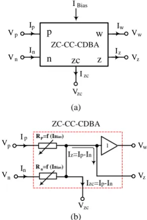
nA with an extremely low voltage supply of 0.65 V. The DC curves Iz,zc versus In and Ip are depicted in Fig. 5.
Thanks to utilizing enhanced BD current mirror, the proposed circuit offers high linearity of Iz versus In and Ip
with extremely low current offset whose value is less than 0.05 µA. The DC curves Iz versus Ip for various values of
In are shown in Fig. 6, whereas the current In vary from -3
µA to 3 µA with a step of 1 µA.
Figure 5. DC curves Iz, Izc versus Ip and In.
The frequency responses of the current gains Iz,zc/In and
Iz,zc/Ip are shown in Fig. 7. The current gains are unity at
low frequencies. The cutoff frequencies of these gains are 2.4 MHz and 5.15 MHz of Iz,zc/In and Iz,zc/Ip, respectively.
The frequency dependence of the parasitic impedance of the z terminal is shown in Fig. 8. The impedance of z terminal is very high about 2.67 MΩ at low frequencies.
Figure 7. Frequency responses of the current gains Iz,zc/Ip, Iz,zc/In.
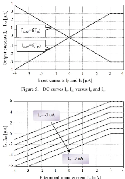
The DC curve Vz versus Vw is shown in Fig. 9. Besides,
the voltage error (Vz-Vw) is depicted. The high linearity
and the wide range operation can be observed. Furthermore, in the range from 0.04 V to 0.58 V, the voltage error is less than 1 mV.
Figure 8. Frequency response of the parasitic impedances of z and zc terminals.
Figure 9. DC curves Vw versus Vz and the voltage error Vz-Vw.
The frequency response of the voltage gain Vw/Vz is
clarified in Fig. 10. The AC simulation is performed using capacitive load of 1pF. The cutoff frequency is 11.18 MHz with unity gain at low frequencies.
The frequency response of the parasitic impedance of w terminal is depicted in Fig. 11. The value of this impedance at low frequencies is 1 kΩ. The most important features of the proposed ZC-CC-CDBA are listed in Table II.
Figure 10. AC curve of the voltage gain VW/VZ.
The power consumption of the proposed circuit is extremely low (5.6 µW to 56 µW) for (IBias=1 µA to
IBias=10 µA), respectively.
Figure 11. Frequency dependence of the parasitic impedance of w terminal.
TABLEII.THE MOST IMPORTANT CHARACTERISTICS OF THE CIRCUIT IN FIG.2
Parameter Value
Voltage supply,bias current 0.65 V, 3 µA Power consumption for IBias=3 µA 17 µW
3 dB bandwidth of Iz,zc/Ip, Iz,zc/In 5.15 MHz, 2.4 MHz
Current offset <50 nA Current gains Iz,zc/Ip, Iz,zc/In 1, 1
3 dB bandwidth of Vw/Vz 11.18 MHz
voltage gain Vw/Vz 1
Voltage offset <1 mV Resistance of terminal Z 2.67 MΩ Resistance of terminal w 1 kΩ
B. Simulation Results of the Current Mode Biquad Filter Based on ZC-CC-CDBA:
The simulation results of the multi-function current mode biquad filter shown in Fig. 4 are depicted in Fig. 12, 13 and 14. The three ZC-CC-CDBAs are biased by IB1=IB2=IB3=1 µA. The components of the filter are C1=5
nF and C2=10 nF. That yields the pole frequency of 950
shown in Fig. 4 are presented in Fig.12 for Rload=1 Ω. It is
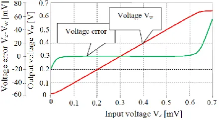
obvious that this filter can provide low pass, band pass and high pass functions simultaneously, without any change in the circuit topology. The band pass gain responses for various values of IB1 are depicted in Fig. 13.
It can be observed that by adjusting the Rp1 value via IB1,
the quality factor can be tuned independent from the pole frequency as it was clarified in (7) and (8). Moreover, Fig. 14 depicts the band pass filter gain responses for (IB1=IB2=IB3=0.5 µA, 1 µA and 1.5 µA), it is noticeable
that the pole frequency can be adjusted without affecting the quality factor as it was described in (7) and (8).
Figure 12. Frequency response of the proposed filter.
Figure 13. The response of the band pass filter for different IB1 values.
Figure 14. The response of the band pass filter for different values of IB1,
IB2 and IB3.
V.CONCLUSIONS
This paper presents a new ULV LP bulk driven based ZC-CC-CDBA capable to operate under single supply voltage of only 0.65 V. Besides, the proposed circuit
enjoys circuit simplicity, high linearity, extended output voltage range and tunable parameters. Furthermore, additional copy of the difference current (Ip-In) is
available through zc terminal. This additional terminal solves the problem of utilizing output current to drive the working impedance directly. Eventually, as an example of application a multi-function current mode filter is presented to prove the functionality of the proposed circuit. Thanks to the tunable parameters of the circuit the quality factor and the pole frequency are adjustable independently.
ACKNOWLEDGMENT
The described research was performed in laboratories supported by the SIX project; the registration number CZ.1.05/2.1.00/03.0072, the operational program Research and Development for Innovation and has been supported by Czech Science Foundation project No.: P102-14-07724S.
REFERENCES
[1] F. Silveira and D. Flandre, Low Power Analog CMOS for Cardiac Pacemakers: Design and Optimization in Bulk and SOI Technologies, Kluwer Academic Publishers, 2004.
[2] S. Yan and E. Sanchez-Sinencio, “Low-voltage analog circuit design techniques, a tutorial,” IEICE Trans. Analog Integr. Circuits Syst., vol. E00-A, no. 2, pp. 179-196, 2000.
[3] S. S. Rajput and S. S. Jamuar, “Low voltage analog circuit design techniques,” IEEE Circuits Syst. Mag., vol. 2, no. 1, pp. 24-42, 2002.
[4] F. Khateb, S. B. A. Dabbous, and S. Vlassis, “A survey of non-conventional techniques for low-voltage low-power analog circuit design,” Radioengineering, pp. 415-427, 2013.
[5] A. Guzinski, M. Bialko, and J. C. Matheau, “Body-driven differential amplifier for application in continuous-time active C-filter,” in Proc. ECCD, Paris, France, 1987, pp. 315-319. [6] T. Kulej, “0.5-V bulk-driven OTA and its applications,” Circuits
Theory and Application J., pp. 1–18, 2013.
[7] F. Rezaei and S. J. Azhari, “Ultra low voltage, high performance operational transconductance amplifier and its application in a tunable Gm-C filter,” Microelectron. J., vol. 42, pp. 827-836, 2011.
[8] J. M. Carrillo, G. Torelli, R. Pérez-Aloe, J. M. Valverde, and J. F. Duque-Carrillo, “Single-pair bulk-driven CMOS input stage: A compact low-voltage analog cell for scaled technologies,”
Integration VLSI J., vol. 43, no. 3, pp. 251-257, 2010.
[9] G. Raikos and S. Vlassis, “0.8V bulk-driven operational amplifier,” Analog Integrated Circuits and Signal Processing, pp. 425-432, 2010.
[10] Y. Haga and I. Kale, “Bulk-driven flipped voltage follower,” in
Proc. IEEE ISCAS, 2009, pp. 2717–2720.
[11] S. Vlassis and G. Raikos, “Bulk-driven differential voltage follower,” Electron. Lett., vol. 45, pp. 1276-1277, 2009.
[12] F. Khateb, N. Khatib, and D. Kubánek, “Novel voltage low-power high-precision CCII± based on bulk-driven folded cascode OTA,” Microelectron. J., vol. 42, pp. 622-631, 2011.
[13] G. Raikos, S. Vlassis, and C. Psychalinos, “0.5 V bulk-driven analog building blocks,” AEÜ, Int. J. Electron. Commun., vol. 66, pp. 920-927, 2012.
[14] F. Khateb and D. Biolek, “Bulk-driven current differencing transconductance amplifier,” Circuits Syst. Signal Process, vol. 30, pp. 1071-1089, 2011.
[15] F. Khateb and S. Vlassis, “Low-voltage bulk-driven rectifier for biomedical applications,” Microelectronics J.,vol. 44, no. 8, pp. 642-648, 2013.
[16] F. Khateb, F. Kacar, N. Khatib, and D. Kubánek, “High-precision differential-input buffered and external transconductance amplifier for low-voltage low-power applications,” Circuits Syst. Signal Process, vol. 32, pp. 453-476, 2013.
[17] F. Khateb, M. Kumngern, S. Vlassis, and C. Psychalinos, “Differential difference current conveyor using bulk-driven technique for ultra-low-voltage applications,” Circuits, Syst. Signal Process.
[18] F. Khateb, D. Biolek, N. Nabhan, and J. Vavra, “Utilizing the bulk-driven technique in analog circuit design,” in Proc. IEEE 13th International Symposium on Design and Diagnostics of Electronic Circuits and Systems, 2010, pp. 16-19.
[19] E. Rodriguez-Villegas, “Low power and low voltage circuit design with the FGMOS transistor,” 2006.
[20] J. M. A. Miguel, A. J. Lopez-Martin, L. Acosta, J. Ramirez-Angulo, and R. G. Carvajal, “Using floating gate and quasi-floating gate techniques for rail-to-rail tunable CMOS transconductor design,” IEEE Trans. Circuits and Systems, pp. 1604-1614, 2011.
[21] F. Khateb, N. Khatib, and D. Kubánek, “Low-voltage ultra-low-power current conveyor based on quasi-floating gate transistors,”
Radioengineering,vol.21, pp. 725-735, 2012.
[22] V. S. Babu, A. Sekhar, R. S. Devi, and M. R. Baiju, “Floating gate MOSFET based operational transconductance amplifier and study of mismatch,” Industrial Electronics and Applications, pp. 127-132, 2009.
[23] F. Rezvan, and E. Farshidi, “A FG-MOS based fully differential current controlled conveyor and its applications,” Circuits, Systems, and Signal Processing, vol. 32, pp. 993-1011, 2013. [24] F. Khateb, W. Jaikla, M. Kumngem, and P. Prommee,
“Comparative study of sub-volt differential difference current conveyors,” Microelectronics J., pp. 1-7, 2013.
[25] C. Acar and S. Ozoguz, “A new versatile building block: Current differencing buffered amplifier suitable for analog signal-processing filters,” Microelectronics J., vol. 30, no. 2, pp. 157-160, 1999.
[26] W. Tangsrirat and W. Surakampontorn, “Electronically tunable quadrature oscillator using current-controlled current differencing buffered amplifiers,” J. of Active and Passive Electronic Devices, vol. 4, pp. 163-174, 2009.
[27] W. Jaikla, p. Silapan, and M. Siripruchyanun, “A simple quadrature oscillator using only CCCDBAs and grounded capacitors,” Communications and Information Technologies, ISCIT ’07, pp. 234-237.
[28] F. Khateb, W. Jaikla, D. Kubanek, and N. Khatib, “Electronically tunable voltage-mode quadrature oscillator based on high performance CCCDBA,” Analog Integrated Circuits and Signal Processing, vol. 74, pp. 499-505, 2013.
[29] S. Maheshwari and I. A. Khan, “Current controlled current differencing buffered amplifier: implementation and applications,”
Active and Passive Electronic Components, vol. 27, no. 4, pp. 219-227, 2004.
[30] S. E. Oner, M. Koksal, and M. Sagbas, “Electronically controllable biquads using single CDBA,” in Proc. 2006 International Symposium on Circuits and Systems, Kos, Greece, 2006.
[31] M. Siripruchyanun, P. Silapan, and W. Jaikla, “Low-offset BiCMOS current controlled current differencing buffered amplifier (CC-CDBA) and applications,” ECTI Trans. on Electrical Engineering, Electronics, and Communications, vol. 6, no. 1, pp. 81-90, 2008.
[32] M. Siripruchyanun and W. Jaikla, “Current-mode biquadratic filter using DO-CCCDBAs,” International J. of Circuit Theory and Applications, vol. 38, no. 3, pp. 321-330, 2010.
[33] W. Tangsrirat, D. Prasertsom, and W. Surakampontorn, “Low-voltage digitally controlled current differencing buffered amplifier and its application,” International J. of Electronics and Communications (AEU), vol. 63, no. 4, pp. 249-258, 2009. [34] D. Biolek, R. Senani, V. Biolková, and Z. Kolka, “Active
elements for analog signal processing: Classification, review, and new proposals,” Radioengineering, vol. 17, no. 4, pp. 15-32, 2008.
[35] D. Biolek, J. Bajer, V. Biolková, Z. Kolka, and M. Kubíček, “Z copy-controlled gain-current differencing buffered amplifier and its applications,” International j. of Circuit Theory and Applications, vol. 39, pp. 257-274, 2011.
[36] M. Sagbas and M. Koksal, “A new multi-mode multifunction filter using CDBA,” in Proc. 2005 European Conf. on Circuit Theory and Design, Cork, Ireland, 2005, pp. 225-228.
[37] A. U. Keskin and E. Hancioglu, “Current-mode multifunction filter using two CDBAs,” International J. of Electronics and Communications (AEU), vol. 59, no. 8, 2005, pp. 495-498. [38] A. U. Keskin, “Multifunction biquad using single CDBA,”
Electrical Engineering, vol. 88, no. 5, pp. 353-356, 2006. [39] A. U. Keskin, “Voltage mode notch filters using single CDBA,”
Frequenz, vol. 59, no. 9-10, pp. 225-228, 2005.
[40] A. U. Keskin, “Voltage-mode high-Q band-pass filters and oscillators employing single CDBA and minimum number of components,” International J. of Electronics, vol. 92, no. 8, pp. 479-487, 2005.
[41] W. Tangsrirat, T. Pukkalanum, and W. Surakampontorn, “CDBA-based universal biquad filter and quadrature oscillator,” Active and Passive Electronic Components, Article ID 247171, 6, 2008. [42] S. Maheshwari and I. A. Khan, “Novel voltage-mode universal
filter using only two CDBAs,” J. Circuits, Systems and Computers, vol. 14, no. 1, pp. 159–164, 2005.
[43] W. Tangsrirat and S. Pisitchalermpong, “CDBA-based quadrature sinusoidal oscillator,” Frequenz, vol. 61, no. 3-4, pp. 102-104, 2007.
[44] M. Koksal and M. Sagbas, “A versatile signal flow graph realization of general transfer function by using CDBA,”
International J. of Electronics and Communications (AEU), vol. 61, pp. 35-42.
[45] A. U. Keskin, C. Aydin, E. Hancioglu, and C. Acar, “Quadrature oscillator using current differencing buffered amplifiers (CDBA),”
Frequenz, vol. 60, pp. 57-60, 2006.
[46] J.-W. Horng, “Current differencing buffered amplifiers based single resistance controlled quadrature oscillator employing grounded capacitors,” IEICE Transactions on Fundamentals, vol. E85-A, pp. 1416-1419, 2002.
[47] R. G. Carvajal, J. Ramirez-Angulo, A. J. Lopez-Martin, A. Torralba, J. A. G. Galan, A. Carlosena, and F. M. Chavero, “The flipped voltage follower: A useful cell for low-voltage low-power circuit design,” IEEE Trans. Circuits and Systems-I: Regular Papers, vol. 52, no. 7, pp. 1276-1291, 2005.
[48] Wafer Electrical Test Data and SPICE Model Parameters. [Online]. Available: http://www.mosis.com/pages/Technical/Testdata/tsmc-018-prm
Salma Bay Abo Dabbous was born in 1985. She
received the M.Sc. degree in Electronic Engineering from Aleppo University, Syrian Arab Republic in 2008. She is currently a Ph.D. student at the Department of Microelectronics, Brno University of Technology. She has expertise in new principles of designing analog circuits, particularly low-voltage low-power analog circuit design for biomedical application.
Ziad Alsibai was born on May 13, 1984. He