Preparation and Characterization of CdTe Thin Films For
Device Applications
B. N. JAGADALE
Department of Electronics,
Kuvempu University, Shankaragatta-577451, INDIA.
(Received on: October 30, 2012)
ABSTRACT
In the present work, the CdTe thin films of different thickness were prepared in the vacuum chamber using thermal evaporation using vacuum coating unit. The prepared films were cut into pieces and characterized for structural and optical properties. The structural analysis of as prepared samples was carried out by the XRD (PHILIPS PW 3710). The optical properties were studied using UV-Vis spectrophotometer (Model Shimodzu 1650 PC). The structural analysis showed that increase with thickness, crystallanity and grain size increases where as strain and dislocation density decreases. With increase in deposition time, the nucleus size increases leading to larger clusters, their coalescence and formation of continuous films and hence also the grain size of these films. Optical properties reveal that the absorbance of the thicker films is more than that of thinner films. Calculated optical band gap decreases with increase in the film thickness reaching to the theoretical value.
Keywords: Optical band, Thin films, Lattice parameters, absorption coefficient, electrical properties.
1. INTRODUCTION
The aim has been to present the fundamentals of thin films in a simple and logical manner through keeping link and continuity amongst different topics dealt in different chapters. A casual comparison of film behavior and physic-chemical characteristics revealed the sensitivity of
the world war because of numerous applications in the diverse fields such as electronic industries, military weapon systems, space science, solar energy utilization, optical and superconducting films, high memory computer elements, sensors, microelectronic and hybrid circuits and others. Due to such vast applications researches are going on not only in the field of basic thin film physics, but also in material science, thin film circuit designs, production engineering concerning thin films, etc. to cop up the demand of industries.
The structural, optical and electrical properties of thin films mainly depends on the deposition parameters such as: rate of deposition, substrate temperature, environmental conditions, residual gas pressure in system, purity of material to be deposited, inclusion of foreign matter in the deposit, in-homogeneity of the film, structural and compositional variations of film in localized and wider area. A transition from bulk to thin film state may even cause drastic change in its properties. Such as highly conducting sodium, potassium, rubidium, also gold, platinum etc. having positive temperature coefficient of resistance (TCR) in bulk form shows negative TCR in thin film states thus behaving as semi conducting films. Bulk bismuth and antimony which are metallic in nature behave as semiconductors in thin film state.
In view of these, present work constitutes an effort to fabricate & to study the structural and optical properties of most important II-VI compound semiconductor viz. Cadmium Telluride (CdTe) thin films. Therefore the results obtained would help us to assess the structural and optical properties
of CdTe thin films prepared at different thickness for device applications. The II–VI semiconductors, such as CdTe and ZnTe, have drawn scientists’ attention for a long time as perspective materials to produce a wide range of devices for microelectronics. Cadmium telluride single crystals are used as X-ray and gamma radiation detectors, whereas CdTe thin films can be used as base layers in converters of solar energy.
2. OPERATION OF COATING UNIT
First the Hind High Vacuum Coating unit is switched and Rotary pump is switched on. The vacuum chamber and the Air admittance valve are closed. The roughing valve is opened. Now the pirani gauge is switched on and roughing is maintained till the reading is reached 0.05 mbar. After reaching rough vacuum, valve is switched to backing. Now a constant water supply is maintained and all the side doors are closed. Diffusion Pump (DP) is switched on, it takes half an hour to heat, at this stage we can open the vacuum chamber. If opened, the above steps are repeated. When the Silicon Oil gets heated the high vacuum valve is opened. When the penning gauge reading is 2x10⁻⁵ mbar CB1 and rotary drive are switched on. Now the rotary drive is controlled by rd control. Current is maintained by controlling the LT /HT controller. Thickness of the film is noted in the thickness monitor. This process is continued till the required thickness is obtained.
3. PREPARATION OF CdTe SEMICONDUCTOR THIN FILM
Company, Bangalore) Model 12A4D. Pure CdTe (Sigma Aldrich, 99.99%) was used as a source material for the evaporation. The material was placed into molybdenum boat with a small dimple at the center to act as a point source. Cleaned glass slides were used as a substrate. The source-substrate distance was maintained at 13.5 cm. Rotary drive was used to obtain the uniform coating. The rate of evaporation was maintained at ~1.4 Å/sec under the vacuum of 1×10⁻⁵mbar. All the films were prepared at 150°C substrate temperature. Rate of evaporation and thickness were measured using Digital Thickness Monitor (Model DTM 104) fixed to the unit. All the samples were prepared for different thickness with similar deposition conditions.
4. RESULTS AND DISCUSSION
The structural analysis of as prepared samples was carried out by the XRD (PHILIPS PW 3710). The optical properties were studied using UV-Vis spectrophotometer (Model Shimodzu 1650 PC).
5. STRUCTURAL PROPERTIES OF CdTe THIN FILMS
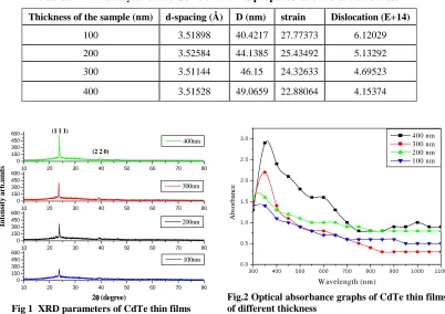
Structural analysis of the prepared samples was carried out by X-Ray diffractometer. XRD patterns of CdTe films for different thickness are shown in fig.4.1. The presence of peak at 2θ=23.76º in (111) direction reveals that all the films are crystalline in nature. The observed values in the XRD and those of JCPDS (ICDD No. 89-3053) data is found in fair agreement between them. All the films have cubic structure with face centered lattice with
lattice constant 6.480Å. It can be seen from the XRD graph that the peak intensity of the films increases with increase in the thickness. The lattice parameters of the films were calculated using the Bragg’s formula:
λ
θ
n
d
sin
=
2
(1)The grain/crystallite size of the films were calculated from the XRD using Scherer’s relation,
θ
β cosλ
k
D = (2)
Where k = 0.94 is a constant, λ - the wavelength of radiation, β - the full width half maximum and θ - the diffraction angle. The micro strain (ε) and the dislocation density (δ) estimated using the equations 3 & 4 and presented in table
(
)
4 cos θ β
ε = (3)
2
1 D
=
δ (4)
It can be noticed from the table that grain size increases with increase in film thickness. Strain and dislocation densities decreases with increase in film thickness.
OPTICAL PROPERTIES
will be helpful for the optoelectronic device applications prepared using thin film technology especially for solar cells.
From the absorbance data, the absorption coefficient was calculated using Lambert law: Fig.2 Optical absorbance graphs of CdTe thin films of different thickness.
d Abs I
I
α
= =
303 . 2
ln 0 (5)
Abs is optical absorbance, IO & I are
intensities of the incident & transmitted radiation respectively α is absorption
coefficient and d is thickness of the films (cm).
The optical band gap Eg was determined by relation,
(
υ
)
υ
α
=
k
h
−
Eg
n/2/
h
(6)Where k is a constant and n is a constant which is equal to one for a direct-gap material. Plots of (αhν) 2 versus hν were
drawn using the equation 5. Extrapolation of the linear portion of the plot to the energy axis yielded the direct band gap value as shown in Fig. 3. It can be observed that energy gap decreases with increase in the thickness.
The direct band gap approaches its bulk value (1.5eV) with increase in thickness for CdTe thin films is found to be 2.24eV. Decrease in Eg with increase in film thickness is due to increase in particle size and decrease in strain.
Table.1 XRD analysis of the CdTe thin films prepared at different thickness
10 20 30 40 50 60 70 80
0 150 300 450
60010 20 30 40 50 60 70 80
0 150 300 450
60010 20 30 40 50 60 70 80
0 150 300 450
60010 20 30 40 50 60 70 80
0 150 300 450 600
2θθθθ (degree)
100nm 200nm (1 1 1)
300nm
In
te
n
si
ty
a
rb
.u
n
it
s
(2 2 0)
400nm
Fig 1 XRD parameters of CdTe thin films
300 400 500 600 700 800 900 1000 1100 0.0
0.5 1.0 1.5 2.0 2.5 3.0
A
b
so
rb
an
ce
W avelength (nm)
400 nm 300 nm 200 nm 100 nm
Fig.2 Optical absorbance graphs of CdTe thin films of different thickness
Thickness of the sample (nm) d-spacing (Å) D (nm) strain Dislocation (E+14)
100 3.51898 40.4217 27.77373 6.12029
200 3.52584 44.1385 25.43492 5.13292
300 3.51144 46.15 24.32633 4.69523
1.2 1.3 1.4 1.5 1.6 1.7 1.8 1.9 2.0 0.0
5.0x10¹⁴
1.0x10¹⁵
1.5x10¹⁵
2.0x10¹⁵
2.5x10¹⁵
3.0x10¹⁵
(
α
h
ν
)
2 (
eV
/c
m
)
2
Eg (eV)
400 nm 300 nm 200 nm 100 nm
Fig. 3 Variation of Eg for CdTe thin films prepared at different thicknesses.
CONCLUSIONS
• CdTe thin films were prepared using resistive heating method for different thickness from 100nm to 400nm.
• Structural characteristics were by X-Ray diffractometer and Optical properties
were studied using UV-Vis
spectrophotometer.
• The structural analysis showed that increase with thickness, crystallanity and grain size increases where as strain and dislocation density decreases. With increase in deposition time, the nucleus size increases leading to larger clusters,
their coalescence and formation of continuous films and hence also the grain size of these films.
• Optical properties reveal that the absorbance of the thicker films is more than that of thinner films.
• Calculated optical band gap decreases with increase in the film thickness reaching to the theoretical value.
REFERENCES
1. R. Bhargava, Properties of Wide Band Gap II–VI Semiconductors (The Institution of Electrical Engineers, London, p. 238 (1997).
2. X. Wu, Solar Energy 77(6), 803 (2004)
3. THIN FILMS FUNDAMENTALS by A
Goswami, New age international publications P. Ltd. (2005).
4. S Lalitha, R. Sathyamoorthy, S. Senthilarasu, A. Subbarayan, K. Natarajan, Solar Energy Materials & Solar cells 82, 187-199 (2004).
5. R. Amutha, A. Subbarayan, R. Sathyamoorthy, J of New Materials for Electrochemical Systems 10, 27-31 (2007).
6. H. Hernandez-Contreras, C. Mejia-Garcia, and G. Contreras-Puente, Thin Solid Films 451-452, 203 (2004).
7. K. L. Chopra, Thin Film Phenomena, McGraw-Hill, New York, (1969).