University of Bradford eThesis
This thesis is hosted in
Bradford Scholars
– The University of Bradford Open Access
repository. Visit the repository for full metadata or to contact the repository team
© University of Bradford. This work is licenced for reuse under a
Creative Commons
THE REALIZATION OF SIGNAL PROCESSING
METHODS AND THEIR HARDWARE IMPLEMENTATION
OVER MULTI-CARRIER MODULATION USING FPGA
TECHNOLOGY
Hassan Saleh Okleh Migdadi
PHD
THE
REALIZATION
OF
SIGNAL
PROCESSING
METHODS
AND
THEIR
HARDWARE
IMPLEMENTATION
OVER
MULTI-CARRIER
MODULATION
USING
FPGA
TECHNOLOGY
Validation and implementation of multi-carrier modulation on
FPGA, and signal processing of the channel estimation
techniques and filter bank architectures for DWT using HDL
coding for mobile and wireless applications
Hassan Saleh Okleh Migdadi
B.Sc., M.Sc.
Submitted for the Degree of
Doctor of Philosophy
Faculty of Engineering and Informatics
University of Bradford
2015
i
Abstract
THEREALIZATIONOFSIGNALPROCESSINGMETHODSANDTHEIR HARDWAREIMPLEMENTATIONOVERMULTI-CARRIERMODULATION
USINGFPGATECHNOLOGY
Validation and implementation of multi-carrier modulation on FPGA, and signal processing of the channel estimation techniques and filter bank architectures for DWT
using HDL coding for mobile and wireless applications Keywords
Field-Programmable-Gate-Arrays (FPGAs); Orthogonal Frequency Division Multiplexing (OFDM); Decoded Pseudo Pilot-Data Aided (FDPP-DA); ECG Patient Monitoring System (ECG-PMS). First part of this thesis presents the design, validation, and implementation of an Orthogonal Frequency Division Multiplexing (OFDM) transmitter and receiver on a Cyclone II FPGA chip using DSP builder and Quartus II high level design tools. The resources in terms of logical elements (LE) including combinational functions and logic registers allocated by the model have been investigated and addressed. The result shows that implementing the basic OFDM transceiver allocates about 14% (equivalent to 6% at transmitter and 8% at receiver) of the available LE resources on an Altera Cyclone II EP2C35F672C6 FPGA chip, largely taken up by the FFT, IFFT and soft decision encoder. Secondly, a new wavelet-based OFDM system based on FDPP-DA based channel estimation is proposed as a reliable ECG Patient Monitoring System, a Personal Wireless telemedicine application. The system performance for different wavelet mothers has been investigated. The effects of AWGN and multipath Rayleigh fading channels have also been studied in the analysis. The performances of FDPP-DA and HDPP-DA-based channel estimations are compared based on both DFT-based OFDM and wavelet-based OFDM systems. The system model was studied using MATLAB software in which the average BER was addressed for randomized data. The main error differences that reflect the quality of the received ECG signals between the reconstructed and original ECG signals are established.
Finally a DA-based architecture for 1-D iDWT/DWT based on an OFDM model is implemented for an ECG-PMS wireless telemedicine application. In the portable wireless body transmitter unit at the patient site, a fully Serial-DA-based scheme for iDWT is realized to support higher hardware utilization and lower power consumption; whereas a fully Parallel-DA-based scheme for DWT is applied at the base unit of the hospital site to support a higher throughput. It should be noted that the behavioural level of HDL models of the proposed system was developed and implemented to confirm its correctness in simulation. Then, after the simulation process the design models were synthesised and implemented for the target FPGA to confirm their validation.
ii
Acknowledgment
First and foremost, I would like to thank ALLAH (God) for giving me the Opportunity to expand my knowledge and horizons. I am also grateful to ALLAH (God) for the successful completion of my PhD report. I would also like to thank my parents, my wife, and sons and daughters for their inspiration, without them none of these would even have been possible. They have always been my biggest fans and I appreciate that.
Special thanks and gratitude to my academic advisers Prof R A Abd-AlhameedandDr J M Noras, for giving me the opportunity to conduct the research work under their supervision. Their scientific wisdom and experience have helped me in achieving my research objectives. I will never forget the many opportunities that they gave me in facilities, publications and teaching. They were like old brothers to me so I pray to ALLAH (God) for their more success and achievements to both of them in this life. Last but not least, my deepest gratitude goes to Dr S M R Jones for his valuable advice, help, and support.
My thanks are also extended to my home supervisors Prof Kasim Al-Aubaidy from the Faculty of Engineering, Philadelphia University, Jordan; and Dr Esam A. Qaralleh, Computer Engineering Department, King Abdullah II Faculty of Engineering - Princess Sumaya University for Technology, Jordan; for their support and all the other people in the research laboratories of Bradford University, especially Mr HuthifaObidat and Dr FauziElmegri.
iii
Table of Contents
Abstract ... i
Acknowledgment ... ii
Table of Contents ... iii
Acronyms ... ix
List of Figures ... xiii
List of Tables ... xvii
Chapter 1 Introduction ... 1
1.1 Background ... 1
1.2 Aimsand Objectives ... 3
1.3 Thesis Contribution ... 4
1.4 Organization of the Thesis ... 5
Chapter 2 Digital Hardware Implementation(FPGAConsiderations) ... 7
2.1 Introduction ... 7
2.2 Terminology Definitions ... 8
2.3 Programmable Logic Device’s Evolution ... 9
2.4 FPGA Architecture ...15
2.4.1 Programmable-Logic-Blocks ...15
2.4.2 Programmable-Routing-Channels...19
2.4.3 Other FPGA resources ...21
2.4.4 FPGA configuration memory ...22
2.5 FPGA, Microprocessor, and ASIC ...23
2.5.1 Introduction of IC, ASIC, and FPGA ...23
2.5.2 FPGA and ASIC comparison ...25
2.6 Computer-Aided-Design (CAD) flow for FPGA ...26
2.6.1 Design Entry ...27
2.6.2 Synthesis ...27
2.6.3 Functional Simulation ...28
2.6.4 Fitting ...28
2.6.5 Timing Analysis and Simulation ...29
iv
2.7 Overview of Commercially Available FPGAs ...31
2.7.1 Market Overview ...31
2.7.2 Recent FPGA devices design timeline ...32
2.7.3 Overview of Development kits ...34
2.7.4 Educational Board ...35
2.8 Conclusion ...38
Chapter 3 Multi Carrier Orthogonal Frequency Division Multiplexing ...40
3.1 Introduction ...40
3.2 Single Carrier and Multicarrier Systems ...41
3.3 Orthogonal Frequency Division Multiplexing (OFDM) ...42
3.4 OFDM History ...43
3.5 OFDM Implementation ...44
3.6 OFDM Transmission Technique ...44
3.7 OFDM Transmitter Diagram ...45
3.7.1 Forward Error Correction (FEC) Encoder ...45
3.7.2 Block Interleaver ...48
3.7.3 Mapping...49
3.7.4 Inverse Fast Fourier Transform (IFFT) ...51
3.8 Multipath and Cyclic Prefix ...54
3.8.1 Diversity Receptions ...55
3.8.2 Multipath and OFDM...56
3.9 OFDM in Future ...58
3.10 Conclusion ...59
Chapter 4 Design of a basic FPGA-Based OFDM Transmitter and Receiver using FFT Algorithm ...60
4.1 Introduction ...60
4.2 Why OFDM on FPGA ...61
4.3 Convolutional Encoder Implementation ...62
4.3.1 Design the Convolutional Encoder Model ...62
4.3.2 Simulating the Convolutional Encoder in MATLAB Simulink ...64
4.3.3 Compiling the Convolutional Encoder with Quartus II Software ...65
4.3.4 Configuration the FPGA board to implement the convolutional encoder ...66
v
4.4.1 Design the Block Interleaver Model ...68
4.4.2 Simulating the Block Interleaver in MATLAB Simulink ...69
4.4.3 Compiling the Block Interleaver with Quartus II Software ...69
4.4.4 Configuration the FPGA board to implement the block interleaver ...70
4.5 16-QAM Mapper Implementation ...71
4.5.1 Design the 16-QAM Mapper Model ...71
4.5.2 Simulating the 16-QAM Mapper in MATLAB Simulink ...73
4.5.3 Compiling the 16-QAM Mapper with Quartus II Software ...73
4.5.4 Configuration the FPGA board to implement the 16-QAM mapper...74
4.6 64-Point IFFT Implementation ...76
4.6.1 Design the 64-Point IFFT Model ...76
4.6.2 Simulating the 64-Point IFFT in MATLAB Simulink ...77
4.6.3 Compiling the 64-Point IFFT with Quartus II Software ...79
4.6.4 Configuration the FPGA board to implement the 64-point IFFT model ...80
4.7 OFDM Transmitter using FFT Algorithm Implementation ...81
4.7.1 Design the OFDM Transmitter using FFT Algorithm ...81
4.7.2 Simulating the OFDM using 64-Point IFFT in MATLAB Simulink ...82
4.7.3 Compiling the OFDM Transmitter using FFT Algorithm with Quartus II Software ...83
4.7.4 Configuration the FPGA board to Implement the OFDM Transmitter using FFT Algorithm ...84
4.8 OFDM Receiver using FFT Algorithm Implementation ...85
4.8.1 Design of Viterbi Decoder ...85
4.8.2 Simulating the Soft-Decision Viterbi Decoder in MATLAB Simulink ...87
4.8.3 Compiling the Soft-Decision Viterbi Decoder with Quartus II Software ...88
4.8.4 Configuration the FPGA board to Implement the Soft-Decision Viterbi Decoder ...89
4.9 Full OFDM receiver ...90
4.10 Conclusion ...92
Chapter 5 Channel Estimation for OFDM FFT/DWT in Multi-Carrier Modulation used in Wireless Telemedicine Applications ...93
5.1 Introduction ...93
vi
5.2.1 OFDM ...94
5.2.2 OFDM-FFT versus OFDM-DWT and OFDM-WPT ...95
5.2.3 OFDM FFT/DWT performance evaluation Review ...96
5.2.4 Channel Estimation ...97
5.2.5 Channel Estimation for OFDM-FFT/DWT e Review ...98
5.2.6 Telemedicine ...99
5.2.7 Using of OFDM in Telemedicine Review ... 101
5.2.8 Proposed Work ... 101
5.3 ECG-PMS Model ... 103
5.3.1 Patient site ... 104
5.3.2 Hospital site ... 105
5.4 Configuration of the Basic OFDM Transmission Scheme ... 106
5.4.1 Transmitter ... 106
5.4.2 Receiver ... 108
5.5 Source Data Channel ... 109
5.5.1 AWGN Channel Effect ... 109
5.5.2 Fading Channel Effect ... 113
5.6 FEC and Interleaving ... 117
5.6.1 Effect of FEC on OFDM System ... 117
5.6.2 Interleaving Effect on OFDM System ... 120
5.7 Channel Estimation and Pilot Insertion ... 124
5.7.1 Pilot Insertion Types ... 125
5.7.2 Basic Channel Estimation Technique ... 127
5.8 Modified Channel Estimation Techniques ... 129
5.8.1 Periodic Pilot Insertion Technique... 130
5.8.2 Improved Data-Aided (DA) Technique ... 131
5.9 FEC (Forward Error Correction coding) Decoded Pseudo Pilot (FDPP) Channel Estimation Technique ... 135
5.10 Logarithm of Likelihood Ratio (LLR) Calculation in Soft Decision FEC ... 142
5.11 Simulation Results ... 143
vii
5.11.2 Comparison between FDPP-DA-based channel estimation and HDPP-DA-based channel estimation for DFT-HDPP-DA-based OFDM and Wavelet-HDPP-DA-based OFDM
systems ... 148
5.11.3 Investigation of the effect of the Doppler Frequency on the FDPP-based channel estimation ... 152
5.11.4 ECG-PMS system Evaluation ... 156
5.12 Conclusion ... 159
Chapter 6 DWT and FIR filters Architectures for OFDM system on FPGA ... 160
6.1 Introduction ... 160 6.2 Literature Review ... 161 6.2.1 FT and WT ... 161 6.2.2 DWT ... 162 6.2.3 Link DWT to Filter ... 163 6.2.4 Digital Filter ... 163 6.2.5 Computation of DWT ... 163
6.2.6 DWT and FIR filter and FPGA ... 164
6.2.7 DWT and FIR performances ... 164
6.2.8 Hardware real time ... 165
6.2.9 FIR on FPGA: Convolution and DA ... 165
6.2.10 DWT on FPGA ... 165
6.2.11 Proposed work: DWT in designed health system ... 166
6.3 FIR Digital Filter ... 167
6.3.1 Filter ... 167
6.3.2 Analog Filter and Digital Filter ... 168
6.3.3 IIR and FIR Filters ... 168
6.3.4 Choose between FIR and IIR Filters ... 170
6.4 FIR Implementation ... 171
6.4.1 FIR filter Structure ... 171
6.4.2 Convolutional approach ... 172
6.4.3 Distributed Arithmetic (DA) ... 173
6.5 Simulation, Experiments and Results for FIR implementation ... 178
6.5.1 System parameters ... 178
viii
6.5.3 Experiments 02 ... 179
6.5.4 Experiments 03 ... 180
6.5.5 Conclusions on these Experiments ... 181
6.6 Proposed iDWT/DWT system implementation using DA based FIR filter ... 181
6.7 Simulation, Experiments, and Results for proposed iDWT and DWT architectures ... 184
6.7.1 Pre Experiments ... 184
6.7.2 Experiments ... 188
6.8 Conclusion ... 191
Chapter 7 Conclusions and Recommendations for Future Work... 192
7.1 Summary ... 192
7.2 Summary of the thesis conclusions ... 193
7.3 Suggestions for Future Work ... 195
7.3.1 Design on an FPGA-Based MIMO Transceiver... 195
7.3.2 FPGA application for Location Based Services (LBS) ... 197
Chapter 8 References ... 200
8.1 Bibliography ... 200
ix
Acronyms
3D-IC Three Dimensional Integrated Circuit
AOA Angle of arrival
ASIC Application Specific Integrated Circuit
BER Bit Error Rate
CAD Computer Aided Design
CE Channel Estimation
CLB Configurable Logic Block
CP Cyclic Prefix
CPLD Complex Programmable Logic Device
CTS Child Tracking system
DA DataAided ( in chapter 5)
DA Distributed Arithmetic( in chapter 6)
DFT Discrete Fourier Transform
DSP Digital Signal Processing
DWT Discrete Wavelet Transform
0 b
N
E
BitEnergytoNoiseDensityECG-PMS Electrocardiography Patient Monitoring System
EDIF Electronic Design Interchange Format FDPP FEC (Forward Error Correction coding)
Decoded Pseudo Pilot
x
FEC Forward Error Correction Encoder
FF FlipFlop
FFT Fast Fourier Transform
FIR Finite Impulse Response
FPD Field Programmable Device
FPGA Field Programmable Gate Array FPLA Field Programmable Logic Array
GI Guard Interval
GPS Global Positioning System
HCPLD High Capacity Programmable Logic Device
HDL Hardware Description Language
HDPP Hard Decision Pseudo Pilot
IC Integrated Circuit
ICI InterCarrier Interference
IDFT Inverse Discrete Fourier Transform iDWT Inverse Discrete Wavelet Transform IFFT Inverse Fast Fourier Transform
IIR Infinite Impulse Response
IP Intellectual Property
ISI InterSymbol Interference
LB Logic Block
LE Logic Element
xi
LSI Large Scale Integration
LUT LookUp Table
MCM Multicarrier Modulation
MIMO Multiple Input Multiple Output
MSI Medium Scale Integration
NRE Non Recurring Engineering
OFDM Orthogonal Frequency Division Multiplexing
OFDMA OFDM Access
OTP One Time Programmed
PAL Programmable Array Logic
PDA Parallel Distributed Arithmetic
PLA Programmable Logic Array
PLD Programmable Logic Device
PLTS Patient Location Tracking System
PROM Programmable Read Only Memory
RP ReProgrammed
RSS Received signal strength
SDA Serial Distributed Arithmetic SISO Single Input Single Output
SNR Signal to Noise Ratio
SoC or SOC System Ona Chip
SPLD Simple Programmable Logic Device
xii
TDOA Time Different Of Arrival ULSI Ultra Large Scale Integration VLSI Very Large Scale Integration
WBAN Wireless Body Area Network
WPT Wavelet Packet Transform
WSI Wafer Scale Integration
xiii
List of Figures
Figure 2-1 3×3 Programmable-Read-Only-Memory PROM ... 10
Figure 2-2 Programmable Logic Array (PLA) ... 11
Figure 2-3 Programmable-Array-Logic (PAL) ... 12
Figure 2-4 Programmable-Array-Logic (PAL) with Flip-Flops (FFs)... 13
Figure 2-5 FPGA Structure ... 14
Figure 2-6 Xilinx XC4000 Configurable Logic Block (CLB) ... 17
Figure 2-7 Altera FLEX 8000 Logic Element (LE) ... 18
Figure 2-8 Altera FLEX 8000 Logic Array Block (LAB) ... 18
Figure 2-9 Xilinx XC4000 Wire Segments ... 20
Figure 2-10Architecture of Altera FLEX 8000 FPGAs ... 21
Figure 2-11 CAD flow ... 27
Figure 2-12 PLD market share ... 32
Figure 2-13 FPGA market share ... 32
Figure 2-14 DE2 Development and Education Board ... 36
Figure 2-15DE4 Development and Education Board ... 37
Figure 3-1 FDM System Bandwidth ... 42
Figure 3-2 OFDM System Spectrum ... 42
Figure 3-3 OFDM System Spectrum Overview ... 43
Figure 3-4 OFDM Transmitter Block Diagram ... 45
Figure 3-5 FEC Example... 46
Figure 3-6 State Diagram ... 47
Figure 3-7 Trellis Diagrams ... 48
Figure 3-8 QAM-4 Constellation Map ... 50
Figure 3-9 8 point FFT block Diagram ... 54
Figure 3-10 Cyclic Prefix in OFDM ... 58
Figure 4-1 Convolutional Encoder of rate (2, 1, 4) Design ... 63
Figure 4-2 State Machine Editor ... 63
Figure 4-3 Convolutional Encoder of a rate (2, 1, 4) MATLAB Simulink Result ... 65
Figure 4-4 Allocated Resources for Convolutional encoder of rate (2,1,4) ... 66
xiv
Figure 4-6 Configuration the Convolutional Encoder on Cyclone II FPGA board/example
... 67
Figure 4-7 A 2×2 Block Interleaver Design ... 69
Figure 4-8 Allocated Resources for 2by2 Block Interleaver ... 70
Figure 4-9 Configuration the Block Interleaver on Cyclone II FPGA board ... 71
Figure 4-10 16 QAM constellation with Gray code mapping ... 72
Figure 4-11 16-QAM mapper design ... 73
Figure 4-12 Allocated Resources for 16-QAM mapper ... 74
Figure 4-13 Configuration the QAM mapper on Cyclone II FPGA board ... 75
Figure 4-14 Configuration the 16 QAM mapper on Cyclone II FPGA board/example ... 75
Figure 4-15 64-IFFT Mega Core Design ... 77
Figure 4-16 64-point IFFT MATLAB Simulink Result ... 79
Figure 4-17 Allocated Resources for 64-point IFFT ... 80
Figure 4-18 Configuration the IFFT circuit on Cyclone II FPGA board ... 81
Figure 4-19 OFDM Transmitter -using FFT algorithm- design ... 82
Figure 4-20 OFDM Transmitter -using FFT algorithm- Result ... 83
Figure 4-21 Allocated Resources for OFDM Transmitter using FFT algorithm ... 84
Figure 4-22 Configuration the OFDM Transmitter circuit on Cyclone II FPGA board ... 85
Figure 4-23 Soft-Decision Viterbi Decoder Design ... 87
Figure 4-24 Soft-Decision Viterbi Decoder MATLAB Simulink Result ... 88
Figure 4-25 Allocated Resources for Soft-Decision Viterbi Decoder ... 89
Figure 4-26 Configuration the Soft-Decision Viterbi Decoder on Cyclone II FPGA board ... 90
Figure 4-27 Allocated Resources for OFDM Receiver using FFT algorithm ... 91
Figure 4-28 Configuration the OFDM Receiver using FFT algorithm on Cyclone II FPGA board ... 91
Figure 5-1 ECG Patient Monitoring System (ECG-PMS) - patient site ... 104
Figure 5-2 ECG Patient Monitoring System (ECG-PMS)-hospital/ medical experts’ site ... 104
Figure 5-3Behavior Time Line ... 105
Figure 5-4 Basic OFDM transmission scheme ... 108
xv
Figure 5-6 Average BER versus
E
bN
0 for OFDM-FFT/DWT/DPWT ... 113 Figure 5-7 Basic OFDM transmission scheme under AWGN and Fading channel ... 114Figure 5-8 Average BER performance of Basic OFDM transmission scheme versus 0
b
N
E
... 116Figure 5-9 Basic OFDM transmission scheme employing FEC under Fading and AWGN
... 118
Figure 5-10 Average BER of OFDM employing FEC versus
E
bN
0 under AWGN ... 120 Figure 5-11 Basic OFDM transmission scheme employing interleaving under AWGN and Fading channel ... 121Figure 5-12 Average BER of OFDM employing interleaving versus
E
bN
0 under AWGN... 123
Figure 5-13Transmitted and Received QAM subcarrier ... 124
Figure 5-14 Types of pilot Arrangement for channel estimation ... 125
Figure 5-15 OFDM transmission scheme employing basic channel estimation method 126
Figure 5-16 OFDM packet structure ... 127
Figure 5-17 Maximum Doppler frequency Fd = 500 Hz versus time... 129
Figure 5-18 (a) Packet structure (b) time variance of channel frequency response at a certain subcarrier ... 130
Figure 5-19 Packet structure using periodic pilot insertion for channel estimation ... 131
Figure 5-20 Receiver of OFDM transmission scheme employing a basic periodic DA channel estimation method ... 133
Figure 5-21 Transmitter of OFDM transmission scheme employing FDPP-based channel estimation method ... 137
Figure 5-22 Receiver of OFDM transmission scheme employing a FDPP-based channel estimation method ... 141
Figure 5-23 OFDM transmission scheme Packet Structure ... 144
Figure 5-24 BER performance of OFDM system with the HDPP-based channel
estimation with threshold = 0.4 ... 151
Figure 5-25 BER performance of OFDM system with the FDPP-based channel
xvi
Figure 5-26 BER Performance of OFDM system employing FDPP-based channel
estimation for different sub-packet sizes ... 155
Figure 5-27 Optimum sub-packet size ... 156
Figure 5-28 Transmitted and received ECG signals ... 158
Figure 6-1 Block diagram of a basic filter ... 167
Figure 6-2 A conceptual representation of a digital filter ... 169
Figure 6-3 Direct FIR filter structure ... 172
Figure 6-4 Conventional implementation ... 175
Figure 6-5Distributed Arithmetic implementation ... 175
Figure 6-6Serial DA FIR Filter ... 177
Figure 6-7 DA (with partitioned LUT technique) implementation of the FIR filter ... 177
Figure 6-8 Direct form structure of (a) DWT- decomposition/analysis process (b) iDWT-reconstruction/synthesis process ... 182
Figure 6-9 RTL Schematic Report for fully SDA-based for iDWT... 186
Figure 6-10 RTL Schematic Report for fully PDA-based for DWT ... 186
Figure 6-11 Simulation output for fully SDA-based for iDWT ... 186
Figure 6-12 Simulation output for fully PDA-based for DWT ... 187
Figure 6-13 Area Utilization Fitter Summary report for fully SDA-based for iDWT ... 187
Figure 6-14 Area Utilization Fitter Summary report for fully PDA-based for DWT ... 187
Figure 6-15Fmax. Summary Report for fully SDA-based for iDWT ... 188
xvii
List of Tables
Table 2-1 summary of Programming Technologies ... 22
Table 2-2 FPGA design timeline ... 33
Table 2-3 Altera FPGA families Introduction... 33
Table 2-4 Table Development and Education boards ... 35
Table 2-5 “Board Information” ... 37
Table 3-1 OFDM Mapping Techniques ... 50
Table 4-1 Look-up table for encoder of rate (2, 1, 4) ... 64
Table 5-1 Simulation parametersof OFDM system under AWGN effect ... 111
Table 5-2 Simulation parametersof OFDM system under AWGN and fading effects .... 115
Table 5-3 Simulation parametersof OFDM system employing FEC under AWGN and Doppler frequency effect ... 119
Table 5-4 Simulation parametersof OFDM system employing Interleaving under AWGN and Doppler frequency effect ... 122
Table 5-5 Simulation parametersof OFDM FFT/DWT system employing FDPP and HDPP ... 149
Table 5-6 Simulation parametersof OFDM system employing FDPP under Doppler frequency effect ... 153
Table 5-7 Simulation parametersof ECG-PMS system ... 157
Table 6-1 Coefficient values of DA’s LUT. ... 176
Table 6-2 Filter Synthesis using partly PDA for 8-tap FIR filter ... 179
Table 6-3 Filter Synthesis using partly PDA for 256-tap FIR filter ... 180
Table 6-4 Filter Synthesis using fully SDA for variety-tap FIR filter ... 180
Table 6-5Haar Wavelet coefficients ... 185
Table 6-6 BER for iDWT-DWT model using direct form structure ... 185
Table 6-7 Compassion of Resources Usage, Data Rate and Propagation delay for fully PDA-based for DWT ... 188
Table 6-8 Compassion of Resources Usage and Data Rate for fully SDA-based for iDWT ... 189
1
Chapter 1
Introduction
1.1 Background
Nowadays, highbitrate and high quality service are highly required for many applications in wireless communication area. The Orthogonal Frequency Division Multiplexing (OFDM) scheme has been proposed to tackle these issues and it has been applied widely in wireless communication systems. The OFDM transmission scheme provides robust protection against multipath fading and reduces interference caused by delay spread in wireless mobile environment whilemaintaining low-complexity receiver. OFDM also offershigh spectrum efficiency through the provisionof high date rate transmission capacity and high bandwidth efficiency [1][2][3].
Employing Fast Fourier Transform (FFT) based OFDM in a communications system inevitably yields a reduction in its spectral efficiency caused by guard interval insertion. To remedy this, a Discrete Wavelet Transform (DWT) based OFDM has been proposed. Further, DWT allows signals to overlap in both time and frequency domains, thereby mitigating the detrimental effects of Inter Carrier Interference (ICI) and Inter Symbol Interferences (ISI)[4][5]. Nonetheless, channel estimation is still essentially required in wireless environment due to a numberof
2
factors such as multi-path fading, noise, timing offset, and frequency offset. A channel estimation can be achieved by non-data aided (blind) and data-aided (training)channel estimators. In data-aided (DA), a dynamic channel estimation is realised through sending pilots periodically,yielding reductionin the transmission efficiency. To overcome this, an improved DA algorithm was developed by generating a reference data from the received OFDM symbols[2][5].
Wireless telemedicine hasbecome a hot research field in recent years. Due to the aforementioned wireless channel limitations, an OFDM system has been proposed to be used in such applications to maintain a reliable transmission and reception of biomedical signals[6][7].
There is a large amount of reported work and published papers in the field of OFDMbased information theory and algorithms. However, most of this work has been carried out on using the theoretical approaches and /or simulator and there has been a limited amount of work that focused the attention on the actual practical hardware implementation side of these algorithms in real time systems [8].
Microprocessors, Application Specific Integrated Circuits (ASIC), and Field-Programmable-Gate-Arrays (FPGA) are the three main methodsthat are used to implement digital domain communication systems [9]. Over the last decade, the pre-fabricated and re-programmable silicon devices commonly known as FPGA
3
have evolved to become one of the key digital circuit implementation as they resolved various past challenges in hardware implementation. FPGA is increasingly used nowadays in a wide range of markets including consumer electronics and communications where these markets need different requirements in terms of power efficiency, performance, and cost [10][11][12].
1.2 Aims and Objectives
Currently, a high quality service and a high bit rate are essential for many modern applications of wireless communication and wireless telemedicine applications are not exception. OFDM system has been used to meet these requirements. However, OFDM counteracts multipath fadingand mitigatesits effects, though it does not eliminatesuch effects completely. Thus, channel estimation is essential.For areal time system, more attention must be exerted on the hardware implementation aspect. Consequently, this study is aimed at proposing and investigating a new OFDM system that can efficiently support one of the wireless telemedicine applications requirements, namely, the Electrocardiography Patient Monitoring System (ECG-PMS)presented. To this end, the following objectives are defined:
I. Extensive review of the FPGA technology.
II. DevelopingHDL (VHDL, Verilog) coding skills for FPGA development.
III. Understanding the MATLAB environment and how to programme in MATLAB.
4
V. Simulatingthe convolutional OFDM system using MATLAB software, then implementand configure the OFDM system onto the FPGA chip.
VI. Compiling an overview of the ECG Patient Monitoring System (ECG-PMS) for wireless telemedicine application, and its requirements.
VII. A review on the channel estimation algorithms.
VIII. Designing an OFDM system that meets the ECG-PMS requirements.
IX. Simulatingthe proposed OFDM system using MALTAB,evaluating its viability in different channel scenarios, comparing it with the convolutional OFDM system and evaluating the proposed system performance for different wavelet families
X. Designing an iDWT/DWT system that supports the ECG-PMS requirements, Implementing and configurationit on the target FPGA chip.
1.3 Thesis Contribution
This main contributions of this research work can be summarised as follows: I. A fully functionalOFDM transmitter and receiver implemented using target
FPGA chip has been developed.
II. A DWT-based OFDM with FDPP-DA channel estimation for ECG-PMS system having a significantly high performance quality at hospital site and withstanding a low transmit signal power at patient site (power efficiency enhancement) has been developed.
5
III. Distributed Arithmetic-based (DA) architecturefor 1-D iDWT/DWT system implemented by means of a FPGA chip for effectively supporting the ECG-PMS wireless telemedicine application requirements has been developed.
1.4 Organization of the Thesis
Chapter 2: Digital hardware using FPGAs is introduced in this chapter. After programmable logic devices (PLD) evolution is viewed, the architecture of FPGA is described and then FPGA are compared with Application-Specific-Integrated-Circuit (ASIC). The process from design idea to hardware implementation is described in FPGA’s Computer Aided Design (CAD). Chapter is ended with an overview of the available commercial FPGA.
Chapter 3: An introduction to OFDM is presented in this chapter. After the advantages of multi-carrier over the single-carrier are explained, the main components of OFDM system using FFT algorithm is described and the idea behind using guard-interval with cyclic-prefix is defined and explained how it mitigate the influence of Inter-Symbol Interference (ISI) and Inter-Carrier Interference (ICI).
Chapter4: an FPGA based OFDM implementation is presented in this chapter. Each component of OFDM system is designed using a high-level design software tools providing by Altera and Math-Work, validated, and implemented on Cyclone II FPGA chip. The allocated resources of the available on the target chip are
6
addressed and investigated. The process is repeated for OFDM transmitter and receiver.
Chapter5: in this chapter an ECG Patient Monitoring System (ECG-PMS) for wireless telemedicine applications is presented. An OFDM system is proposed to meet the requirements for the ECG-PMS system, where the requirements at patient site are differ than at hospital site. The OFDM system is designs based on wavelet transform and using FEC (Forward Error Correction coding) Decoded Pseudo Pilot (FDPP) for channel estimation. The proposed system was evaluated using MATLAB software in terms of BER performance and the quality of reconstructed ECG signal.
Chapter6: in this chapter, the proposed implementation for iDWT/DWT system used in OFDM-DWT system for using in the ECG-PMS system is designed using Verilog HDL using ALTERA Quartus II Software (V.13) Environment. Then it validated and implemented on ALTERA EP4CE115F29C7 Cyclone IV FPGA chip on DE2-115 board. The allocated resources on the selected FPGA chip, propagation delay, and the data rate are addressed and compared among wavelet families.
Chapter 7: in this chapter, a conclusions of our research have been summarized and a future works have been suggestions.
7
Chapter 2
Digital Hardware Implementation(FPGA
Considerations)
2.1 Introduction
Over the last decade, Field Programmable Gate Arrays (FPGAs) have become one of the key digital hardware circuit implementation media and has been used in several consumer markets. FPGAs has been used in a wide range of devices targeted at achieving different performance, power efficiency and cost requirements. In addition, FPGAs are pre-fabricated silicon chips that can be electrically programmed to become any designed digital system, using built-in logical elements and programmable connections and can be re-configured ondemand. The exclusion of physical fabrication make marketing designs using FPGA easier than other hardware implementation methods, like ASIC [10][12]. This chapter presents an introduction to digital hardware using FPGAs. It defines the relevant terminology in this field and presentson overview of the evolution of programmable logic devices (PLD). Furthermore, the key elements of the internal structure and architecture of FPGA are discussed. Then a comparison between Application-Specific-Integrated-Circuit (ASIC) and FPGA is performed. The
8
dynamics of a Computer Aided Design (CAD) for FPGA is described, which incorporates the process needed to go from design idea to actual hardware configuration. Finally, commercially available FPGAs are overviewed.
2.2 Terminology Definitions
This section describes the terminology used in this chapter [13]:
Field-Programmable-Device (FPD): describes an integrated circuit (IC) used in an implementation digital hardware, which allows the end user to realize the desired design by configuring the chip. FPD is also referred to as Programmable-logic-devices (PLDs).
Programmable-Logic-Array (PLA): is a small FPD that consists of two logical levels; an AND-plane array followed by an OR-plane array, where both are programmable.
Programmable-Array-Logic (PAL): is a special type of PLA, where the programmable AND-plane array is followed by a non-programmable (fixed) OR-plane array.
Simple-Programmable-Logic-Device (SPLD): is a simple PLD, which is usually either PLA or PAL.
Complex-Programmable-Logic-Device (CPLD): is a more complex PLD, where a multiple SPLD-like blocks are arranged on a single chip. Enhanced-PLD (EPLD), Super-PAL, Mega-PAL are all alternative names for CPLD.
Field-Programmable-Gate-Array (FPGA): is a FPD that allows a very high logic capacity. A FPGA offers narrow logic resources with a high ratio of flip-flops.
9
High-Capacity-Programmable-Logic-Devices (HCPLDs): is types CPLDs and FPGAs in a single acronym.
Inter-connect: refers to the wiring resources of an FPD.
Programmable-Switch: is a switch used to connect an inter-connect wire to a logic element or to another inter-connect wire, where the switch programming is done by the end user.
Logic-Block (LB): a small circuit block, which is replicated and put in an array form, then the array is put inside an FPD. To implement a desired circuit in an FPD, it is decomposed into simple-sub-circuits, where each one can be mapped into one logic-block in an FPD.
Logic-Capacity: refers to “the amount of digital logic that can be mapped into a single FPD”.
Logic-Density: is the number of logic per unit area in a single FPD.
Speed-Performance: refers to “the maximum operable speed of the circuit when implemented in an FPD”, where it is set by the longest delay through any path and by the maximum clock frequency for the combinational and sequential circuits needed to function the circuit correctly respectively.
2.3 Programmable Logic Device’s Evolution
Programmable-Read-Only-Memory (PROM) was the first Programmable-Logic-Device (PLD) that was introduced in 1970. The address lines and data lines for PROM is used as logic circuit inputs and outputs respectively [13][14]. PROM consists of a fixed AND-plane level followed by a programmable OR-plane level,
10
represented in Figure 2.1. Figure 2.1 shows a 3X3 PROM that consists of eight AND gates and three OR gates. In general, for an N inputs PROM, a 2N AND gates
are needed for 2N possible minterms, while logic functions mostly require a few
product terms. Therefore, PROMs represents an inefficient architecture for realizing logic circuits and are rarely used in practice [13][14].
Figure 2-1 3×3 Programmable-Read-Only-Memory PROM
The Field-Programmable-Logic-Array (FPLA) device was introduced in 1995 and aimed at addressing PROM limitations by making both AND-plane and OR-plane arrays programmable. FPLA is also called PLA for short purpose [13][15] As shown in Figure 2.2, inputs or their complements of PLA are fed into the AND-plane array to produce the logical-product-term of any combination of these inputs. Then, the outputs of AND-plane array are fed into OR-plane array to produce the logical-sum-term of any combination of the outputs of AND-plane array. Hence logical functions in sum-of-products form are implemented by PLA [13].
11
Figure 2-2 Programmable Logic Array (PLA)
From the example in [16], it is evident that the number of AND gates is independent of the number of PLA inputs and the number of OR gates is independent of both the number of PLA inputs and the number of AND-plane array outputs [15]. The two levels of configurable/programmable logic in PLA increase the manufacturing difficulty and caused propagation delays, which introduced an increase in manufacturing cost and a decrease in speed-performance respectively. The high cost and low speed are considered the main drawbacks of the PLA [13]. In late 1970s, Programmable-Array-Logic (PAL) devices were developed to overcome the disadvantages of PLA [13][17]. As illustrated in Figure 2.3, the structure of a PAL is opposite to the structure of a PROM. A PAL consists of a programmable AND-plane array followed by a fixed OR-plane array, while PROM
12
consists of a fixed AND-plane array followed by a programmable OR-plane array[17]. Because of this featureonly a single level of programmability feature is available in PAL, hence making PAL’s devices faster than PLA’s [13][17]. Additionally, because ofthe programmability in the AND-plane array, the number of AND gates is independent of the number of PAL’s inputs. The shortcoming of generality caused by fixed-OR-plane array has been addressed by producing numerous variants of PALs with various numbers of inputs and outputs, and varies sizes of OR-gate [13]. To realize sequential circuits, Flip-Flops (FFs) are connected to the outputs of OR-gate as shown in Figure2.4 [13].
13
Figure 2-4 Programmable-Array-Logic (PAL) with Flip-Flops (FFs)
PLAs, PALs, and other small PLDs devices are grouped into a category called Simple-Programmable-Logic-Devices (SPLDs), which are considered to have high speed-performance and low cost [13][18].
As the number of SPLD’s inputs is increased, the size of the programmable-logic-plane-arrays is grown quickly. This strict SPLD architecture led to consider SPLD as an inefficient architecture for high capacity devices [13].
Complex- Programmable-Logic-Devices (CPLDs) were proposed to address SPLDs limitations by integrating multiple SPLD blocks inside one chip with programmable interconnections between them [13][19].
The delay through one CPLD is usually short and predictable because it has little flexibility in its internal architecture. Predictable timing characteristics feature make
14
CPLD ideal for applications require critical control, high-speed-performance control, and high-performance-logic [18]. CPLD are inexpensive and require small amount of power, which make CPLD ideal for battery-operated portable and cost-sensitive applications [18].
A different approach called Field-Programmable-Gate-Array (FPGA) can be used to build FPDs with high logic capacity. FPGAs consists of a two dimensional matrix of uncommitted programmable-logic-blocks (depending upon vendor, these blocks are called different things), a programmable routing matrix of interconnections between the programmable-logical-blocks and Input/output blocks [13][18][20]. Figure 2.5 below shows a Typical FPGA structure [18].
Figure 2-5 FPGA Structure
In addition, FPGA is the only type of FPD that support very high-logic-capacity and only in FPGA the end user performs the FPGA configuration through programming.
15
These main distinction features between FGPA and other types of FPD result in significant shift in the way of designing digital circuits [13].
2.4 FPGA Architecture
Because FPGAs combine the programmability idea of PLDs and uncommitted gate arrays in ASIC architecture, FPGAs are considered the most powerful programmable-logic-devices [20].
The basic structure of FPGAs is array-based. The most common FPGA architecture consists of a two dimensional matrix of programmable-logic-blocks (called Configurable Logic Block (CLB) by Xilinx, and Logic Element (LE) by Altera for example), a two dimensional matrix of programmable-routing-channels and I/O blocks as shown in Figure 2.5 above. The programmable-logic-blocks can be interconnected via the horizontal and vertical programmable-routing-channels[21].
2.4.1 Programmable-Logic-Blocks
Commonly, the programmable-logic-block consist of function generators, storage elements, and dedicated arithmetic logic circuits. A function generator can be configured as a Look-Up-Table (LUT), while a storage element as edge-triggered Flip-Flop (FF) or as level-triggered latches[21][22].
16
An n-by-m LUT is a (2n X m) bit wide memory array where the n-address lines fed
into the memory are the LUT input, and m-data lines output from the memory are the LUT output. Thus, a LUT with n inputs can encode and realize any Boolean function of its n inputs by modelling the Boolean function as a truth table and then programing that truth table directly into the memory. For example, one LUT with 4 inputs can implement any Boolean function of up to 4 inputs. In the modern FPGA devices, LUTs with 4-6 input bits are considered as the significant element in the device[13][22][23].
After 1985, Xilinx offered a new FPGA family called XC4000 series. Figure 2.6 below shows the basic CLB used in XC4000 series. CLB consists of three LUTs, two D-FFs, and other logic components for arithmetic circuit. The two LUTs to the right of the figure are fed by the CLB inputs, while the third one are used to combine the other two LUTs when needed. This structure provides the ability to implement any Boolean functions of up to eight inputs in normal mode or two different Boolean functions each one up to four inputs in arithmetic mode where the selection of the mode is programmed into the other logic components [13][21].
17
Figure 2-6 Xilinx XC4000 Configurable Logic Block (CLB)
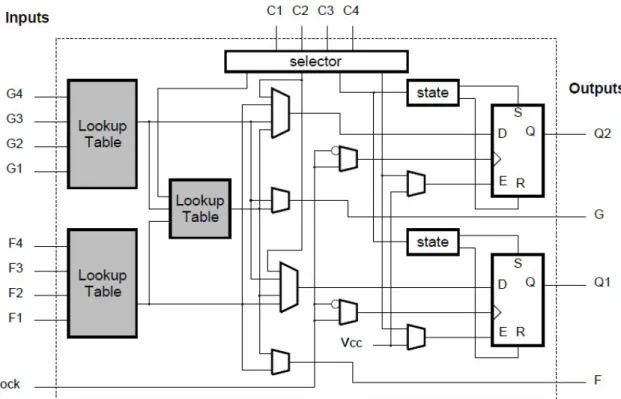
Altera offers another FPGA family called FLEX 8000 series. Figure 2.7 below shows the basic LE used in FLEX 8000 series. LE consists of one 4-input LUT, one SR-FF, and other logic components for arithmetic circuit. The cascade circuit are used to implement a wide AND functions efficiently [13].
18
Figure 2-7 Altera FLEX 8000 Logic Element (LE)
19
In FLEX 8000, Altera grouped each eight LEs in one set called Logic-Array-Block (LAB) as shown in Figure 2.8. Inside each LAB, there is a local interconnect used to connect any LE to any other LE within the same LAB [13].
2.4.2 Programmable-Routing-Channels
To connect logical blocks with each other, a two dimensional matrix of programmable routing channels is used where the structure of this interconnect is considered a significant feature in the FPGA device. Each channel consists of a number of wire-segments, and each wire-segment consists of a number of connection lines. Different types of connection lines are used in FPGAs, for example, to connect distant logical blocks a long connection lines is used, while a short connection lines is used in the case of neighbouring blocks, where for reset all FFs inside the FPGA a reset connection lines is used. Then one of the user-programmable switch technologies is used to connect the wire-segments to the inputs/outputs of the Logical-Blocks, or the wire-segments together [13][24].
Figure 2.9 below shows one of the horizontal-routing-channels, where the vertical-routing-channels, Inputs/Outputs of CLBs, and routing switches are not shown in this figure. The speed-performance of the configured circuit depends on how the CAD tools allocate the wire-segments for each signal. This is because when the signal travels from one CLB to another it needs to pass through a number
20
programmable-switches, where the particulate setting of wire-segments used determine how many switches crossed [13].
Figure 2-9 Xilinx XC4000 Wire Segments
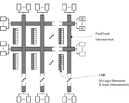
In the Altera FLEX 8000 series, the short connection lines are replaced by using local interconnect inside the LABs, thus only long connection lines extending the total height and width of the FPGA device are needed. These lines are placed in horizontal and vertical tracks called Tracks as shown in Figure 2.10. Fast-Tracks contains only long connection lines have two advantages. First one, number of user-programmable switches are fewer than in the FPGAs that use a number of short wire-segments and therefore the interconnect delays are more Predictable in the FLEX 8000 series. Second advantage, CAD tools can easily implement the desired circuit [13].
21
Figure 2-10Architecture of Altera FLEX 8000 FPGAs
There are many approaches used to implement a user-programmable switch. For example, the user-programmable switch used for CPLDs is the EPROM or EEPROM, while for FPGAs is the antifuse or SRAM. However, the inability of using EPROM/EEPROM in FPGAs could not be explained technically [13].
2.4.3 Other FPGA resources
Contemporary FPGAs contain of other resources in addition to Programmable-Logic-Blocks and Programmable-Routing-Channels such as RAM blocks to implement in-chip data storage, clock management blocks to synthesize numerous clock signals, DSP modules to implement blocks used in digital signal processing algorithms such as digital filters, speed serial transceivers to support a high-speed I/O, and a hardware-CPU or hardware-PowerPC cores [25].
22
2.4.4 FPGA configuration memory
The common programming technologies are shown in Table 2.1 below. From most left, first column names the programing technology, second column describes if the programmable device is a One-Time-Programmed (OTP) or a Re-Programmed (RP), third column indicates the need to configure the device after each power-up(volatile) or not (non-volatile), and the last column lists the name of the transistor technology used in the relative programming technology [13][26][27][28].
Table 2-1 summary of Programming Technologies
Name OTP or RP Volatile Technology
Fuse OTP No Bipolar
EPROM RP, out of circuit No UVCOMS EEPROM RP, in circuit No EECOMS
Antifuse OTP No COMS
SRAM RP, in circuit Yes COMS+
Flash RP No COMS+
Upon configuration memory, FPGAs can be categorised into the following:
a) antifuse-based FPGAs where Actel is one of the leading manufactures for this type. However, the main weakness of these FPGAs is that it can be programmed only once, they are the least susceptible to radiation effect [13][26].
b) SRAM-based FPGAs. For SRAM-based products, Altera and Xilinx are the leading manufactures and offers challenging products. This type of FPGAs can be
23
re-programmed, but because It is a volatile device, it needs to re-configure after each power-up [13][26].
c) SRAM-based FPGAs with integrated Flash. The configuration data are stored in the internal Flash memory inside the FPGA which is used to configure the SRAM during power-up. Therefore, there is no need for external memory [13][26].
d) Flash-based FPGAs. The main manufacture for this type of FPGA is Actel. Power consumption of this type is much less than of the normal SRAM-based FPGAs [13][26].
In the last two decades, these devices have been changed and improved dramatically and Altera and Xilinx offer many new FPGA families with better performance, power efficiency and cost. The architecture of the Cyclone II FPGA chip used in this project is explained in [29].
2.5 FPGA, Microprocessor, and ASIC
2.5.1 Introduction of IC, ASIC, and FPGA
“An integrated circuit (IC) or monolithic integrated circuit (also referred to as IC, chip, or microchip) is an electronic circuit manufactured by the patterned diffusion of trace elements into the surface of a thin substrate of semiconductor material.
24
Additional materials are deposited and patterned to form interconnections between semiconductor devices.” [30].
IC can be classified into three generations according to some factors such as the number of transistors. In first generation small-scale-integration (SSI) was developed then medium-scale-integration (MSI), and finally large-scale-integration (LSI). Then very-large-scale-integration (VLSI) was developed in the second generation. In the last generation ultralargescaleintegration (ULSI), waferscale -integration (WSI), system-on-a-chip (SoC or SOC), and three-dimensional-integrated-circuit (3D-IC) was developed [30].
A special kind of IC are FPGA and Application-Specific-Integrated-Circuit (ASIC) where IC have been developed for general-propose use, while FPGA and ASIC made-to-order for a particular use. An ASIC contains huge number of logical gates just as a FPGA does. Also modern ASICs include other large hard building blocks such as processor blocks, memory blocks (like flash, ROM, and RAM) and other blocks just like FPGAs. Hardware-Description-Language (HDL), like Verilog or VHDL is used to configure the desired circuit on ASIC by engineer designer the same as on FPGAs [21][31].
Both ASIC and FPGA are ICs designed to be configured by the engineer designer after manufacturing using HDL. However, FPGA contains re-configurable logical blocks and interconnects that provide the ability to all/partial re-configuration and
25
update the functionality of the all/portion of the design circuit on the FPGA device after shipping unlike ASIC. The re-configuration feature is considered the main different feature between FPGA and ASIC [21][31].
2.5.2 FPGA and ASIC comparison
This section presents the differences between FPGAs and ASICs in terms of logic density, power consumption, circuit speed, non-recurring engineering (NRE), time to market, cost ( i.e. Area), and re-configuration to enable engineer designers to make better informed choices between FPGA and ASIC media [21][32].
Historically, compared to FPGAs, ASICs offer many advantages including reduced in silicon area, reduced in power consumption, and increased in performance. However, these advantages come at the cost of an increase in non-recurring engineering, an increase in time to market, and inability to re-programme in the field for debugging when designs are implemented on ASICs [21][32].
On the other hand, modern FPGAs contain large hard building blocks like multiplier/accumulator and memory blocks which significantly increase the energy efficiency, decrees the critical path delay and the area. Thus the gap between FPGA and ASIC in term of logic density, power consumption, circuit speed is reduced [21][32].
26
Also, when the ASIC designed functions become part of the manufacture’s Intellectual Property (IP) and can re-used, they are incorporated into their FPGAs to reduce the overall cost of development, manufacturing, and test of the FPGAs and hence the board space, power, and money are saved which leads to a more reduction in the gap between FPGA and ASIC [33].
To conclude, FPGA makers succeed in their seeking to improve FPGAs which is achieved specially by designing a hardware of mixed heterogeneous blocks such as multiplexers, accumulators, multipliers, and memories which are less programmable but more efficient where most modern FPGAs use them [32].
2.6 Computer-Aided-Design (CAD) flow for FPGA
It is essential to make use of Computer-Aided-Design (CAD) programs and tools when implementing desired circuits in FPDs such as SPLDs, CPLDs, and FPGAs [13]. A general typical CAD flow for implementing the designed circuits in FPDs is shown in the Figure 2.11 below [34].
Certain algorithms are used to optimize the desired circuit by the end user manually without using CAD system. This is because mostly the initial logic entry is not in an optimization form. Because this task is done manually by the end user without using CAD system, it is not included in the Figure 2.11 above [13].
27
Figure 2-11 CAD flow
2.6.1 Design Entry
The optimized desired circuits are carried out by more than one method. It can be carried out by creating a schematic diagram using graphical CAD programme when we have simple designs. Or it can be carried out by describing the optimized desired circuits in hardware description languages like VHDL and Verilog using text based system for more complex designs [13][34][35].
28
After design entry, the HDL (VHDL/Verilog) code is converted by the synthesiser to produce the intermediate representation of the hardware design called netlist, where the contents of netlist –which is independent on the specifics of the FPGA-are stored in a standard format named Electronic Design Interchange Format (EDIF). Then the design logic is implemented in devices resources such as logic blocks provided in a FPGA chip by technology mapping [34][35][36][37].
2.6.3 Functional Simulation
Two stages of simulation are used for verifying a design: functional simulation and timing simulation. Functional simulation is performed before fitting task, while timing simulation is performed after fitting task. After synthesis task, the functional simulation is performed, where the functional correctness of the synthesised circuit as it is being designed is verified in this stage. Functional simulation simulates the behaviour of the desired circuit without timing information, it does not take into account the timing properties of the logical blocks and inter-connection-wires inside the FPGA chip, they are assumed ideal and therefore the signal propagates through the circuit without propagation delay. Because of that, functional simulation stage takes much less time than timing simulation stage [34][35][38][39].
2.6.4 Fitting
In fitting, the EDIF netlists produced in synthesis stage is translated into the placed and routed FPGA design. The fitting task consists of four phases: translation,
29
mapping, placement, and routing. In translation phase, the EDIF netlist is converted to a FPGA’s manufacturer netlist format and produce its design file. Using a map program, the logical structures of the design file described in the FPGA’s manufacturer netlist are mapped into available resources in the actual selected FPGA chip such as logical-blocks, flip-flops, RAMs, and LUTs and the output of this phase are stored in another netlists. Then, the placement of the resources like logical-blocks defined in the incoming netlists from mapping phase is determined into the resources in the actual chosen FPGA chip. After that, the essential routing wires in the actual chip required to establish a connection between these particular resources are selected. Placement and routing phases -which mostly are performed by one program, defines how the resources of FPGA chip are placed and interconnected inside the actual chosen FPGA chip. These two phases are considered the most important and time consuming phases in fitting task. However placement phase is more important than routing phase because good placements result in possible good routing and bad placement may result in unattainable good routing. At the end of this task, a generation of a programming file is created and stored in a bitstream format, where this binary data are used in the next task. Some company merges more than one phase together, for example translation and mapping phases are combined into one phase and executed by one programme called quartus_map[34][36][40].
30
In timing analysis, the timing properties of the logical blocks and inter-connection-wires inside the FPGA chip are taken into account. Therefore, an indication of the expected performance of the desired circuit is provided by analyzing all propagation delays the length of the different paths inside the fitted circuit. Then the time simulation is performed where both functional correctness and timing of the fitted circuit as it is being designed is verified. This task is considered as the closet emulation to actually implementation of the desired circuit into the selected FPGA device by providing the behaviour of the desired circuit when it is actually downloaded onto the chosen chip. Thus, it allows the designer to verify that behaves, functional requirements, and timing requirements of the implemented circuits meets the expected one and solve the problems when it happened before the actually implementation. Time simulation and analysis takes more time than functional simulation, but it is more accurate [34][35][39][41].
2.6.6 Programming and Configuration
The bitstream file is loaded into the chosen FPGA device. Thus, the configuration switches inside the chosen FPGA -which is responsible for the configuration logical-blocks and establishing the required inter-connect wiring connections- are programed. Therefore, the desired circuit is implemented into a physical chosen FPGA chip. Because of that, the execution and testing of a desired hardware design is provided by the FPGA chip at the end of this task [34][35].
31
2.7 Overview of Commercially Available FPGAs
2.7.1 Market Overview
By looking at the current PLD/FPGA market figures, we found that the competition is bitter and Ironic. Figure 2.12 show that Xilinx controls over 50% of the PLD market and while Altera control about 35%. Also in FPGA market share, both Xilinx and Altera control over 80% of the FPGA market, where Altera alone controls about 30% as shown in Figure 2.13 [42]. Therefore, to provide a more focused discussion, only the main FPGA manufactures (i.e Xilinx and Altera) whose products are currently widespread are mentioned in this section [13].
Both Xilinx and Altera work on the following two main approaches to expand the FPGAs’ market:
a) Low-End-Market by reducing the per-FPGA-unit-production-cost. b) High-End-Market by increasing the per-FPGA-unit-production-capacity.
The First approach; per-FPGA-unit-production-cost; can be achieved through many methods, such as by using 90 nm technology, 300 mm wafers, and by designing a less processing, less memory FPGAs. However, the second approach; per-FPGA-unit-production-capacity; is needed in applications, where high performance DSP are required, an embedded processing and a high-speed I/O [43].
32
Figure 2-12 PLD market share
Figure 2-13 FPGA market share
2.7.2 Recent FPGA devices design timeline
The manufacturers of FPGAs provide a wide range of device series. Altera offers Cyclone series at the Low-End to provide lowest cost and power FPGAs, and offers Stratix series at the High-End to provide High-End FPGAs. For a Mid-Range FPGAs, Altera offers Arria series to provide a balanced cost, power, and
33
performance FPGAs. While Xilinx offers Artix, Virtex, and Kintex at the Low-End, the High-End, and the Mid-Range FPGAs respectively [43][44][45].
Table 2-2 FPGA design timeline
Altera Xilinx High-End FPGA series Stratix Virtex Mid-Range FPGA series Arria Kintex Low-End FPGA series Cyclone Artix
Table 2-3 Altera FPGA families Introduction Altera Device Family Year of
introduction Process technology Recommended for new designs? Stratix Stratix 2002 130 nm No Stratix GX 2003 130 nm No Stratix II 2004 90 nm Yes Stratix IIGX 2005 90 nm Yes Stratix III 2006 65 nm Yes Stratix IV 2008 40 nm Yes Stratix V 2010 28 nm Yes Arria Arria GX 2007 90 nm Yes Arria II GX 2009 40 nm Yes Arria II GZ 2010 40 nm Yes
Arria V 2011 28 nm Yes
Cyclone Cyclone 2002 130 nm Yes Cyclone II 2004 90 nm Yes Cyclone III 2007 65 nm Yes Cyclone IV 2009 60 nm Yes Cyclone V 2011 28 nm Yes
34
Table 2.3 shows that Cyclone and Artix series are direct competitors, same as Stratix and Virtex series, and as Arria and Kintex[43][44][45].
Table 2.4 shows the year of introduction, process technology, and if it is recommended for new designs for each family for the three series for Altera. More details such as common features for each family can be found in [46][47][48].
2.7.3 Overview of Development kits
In many cases there is no better way to create, implement, and evaluate a design than with a pre-existing platform from FPGA’s manufacturers or one of their development kit partners. FPGA manufacturerdevelopment kits come with everything needed to easily develop and test a system design in a wide range of applications, devices and technologies [49].
Altera and their partners provide a wide variety of development kits that help engineer to simplify the design process and reduce time-to-market [50]. Reference [50] gives us a complete list of the development kits available today and a detail list of the content we will receive on the kit. The documentation that comes with the developments kits make it easy and fast to get the kit working [49].
End market solutions are designed to target an inter-product platform. In reference [51] we can see a complete list of end-markets which Altera provides for specific
35
solution. Some example end markets include wireless, wireline, broadcast and many others. This reference [51] can help us to decide which Altera device is best situated for our system, which reference designs and IP use, and which literature is available [49].
2.7.4 Educational Board
Altera provides a variety of development and education boards designed to meet educational and researchable needs that help students (undergraduate and researcher) to simplify the design process from simple tasks that clarify essential concepts to complex designs needed to prove a novel proposal [52][53][54][55]. Table 2.5 shows the available educational and researchable boards provided by Altera [52].
Table 2-4 Table Development and Education boards
Name Usage FPGA
device Ne w/ O ld I/O feature set Notes Ho m e st ud y Un de rg ra du at e co ur se s gr ad ua te pr oj ec ts Re se ar ch Te ac hi ng pu rp os
e DE0 Yes Yes Cyclone III old Reduce d
A smaller version of DE1 DE0- Yes Yes Cyclon new * A/D converter
36
Nano e IV
DE1 Yes Cyclon
e II new
Reduce d
A smaller version of DE2 DE2 Yes Yes Cyclon
e II old Rich DE2-70 Yes Yes Cyclon e II old Rich DE2-115 Yes Yes Cyclon e IV new Rich Re se ar ch pu rp os
e DE3 Yes Yes Stratix III old High speed
DE4 Yes Ye s Stratix IV new High speed * Suitable for mobile projects.
Altera DE2 development and Education board shown in Figure 2.14 was designed by professors for university and college laboratory use and Altera DE4 development and education board shown in Figure 2.15 was designed to be an excellent research platform [53][55].
37
Figure 2-15DE4 Development and Education Board
Table 2.6 below shows the main features for DE2, DE3, and DE4 education board. Table 2-5 “Board Information”
DE2 DE3 DE4
Feature
FPGA device Cyclone II with EPCS16 16-Mbit serial configuration device Stratix III with EPCS128 128-Mbit serial configuration device Stratix IV with EPCS128 128-Mbit serial configuration device Clock 50 MHz clock 27 MHz clock 50 MHz clock 50 MHz clock 100 MHz clock External SAM clock input
External SAM clock input
External SAM clock output
External SAM clock input
External SAM clock output Memory 8 MB SDRAM 512 SRAM 4 MB Flash 2 MB SSRAM 64 MB Flash SD memory card slot
SD memory card slot DDR2 memory slot
SD memory card slot DDR2 memory slot I/O Interfaces
38
Built-in USB-Blaster for FPGA
configuration
Yes Yes Yes
Line In/Out,
Microphone In (24-bit Audio CODEC)
Yes
Video Out (VGA 10-bit DAC) Yes Video In (NTSC/PAL/ Multi-format) Yes RS232 Yes
Infrared port Yes PS/2 mouse or
keyboard port
Yes
Ethernet Port Yes (10/100) Yes (Gigabit ) USB 2.0
(type A and type B)
Yes Yes Yes
Expansion headers (two 40-pin headers)
Yes Yes Yes
HSMC high-speed headers
Yes Yes
Serial ATA Port Yes
PCI Express x8 Edge Connector
Yes
2.8 Conclusion
This chapter has explored many issues in the world of FPGA architecture, CAD, and commercial availability, which has helped the completion of the rest of this
39
report. Comparison between FPGA and other hardware outcome that are strongly recommended to use FPGA for high-speed digital applications was also performed.
40
Chapter 3
Multi Carrier Orthogonal Frequency Division
Multiplexing
3.1 Introduction
High-bit-rate with high-quality-service is expected from current wireless communication systems. However, in such systems, transmitting data at a high-bit-rate leads to delayed waves, which in turn causes interference problems. Interestingly, Orthogonal Frequency Division Multiplexing (OFDM) transmission scheme was proposed in a bid to overcome this interference problem. OFDM converts a high-bit-rate data streams into low-bit-rate data stream, which are then multiplexed using Frequency Division Multiplexing (FDM). The influence of Inter-Symbol Interference (ISI) and Inter-Carrier Interference (ICI) can be mitigated but not eliminated completely, by inserting a guard interval with cyclic prefix. Hence, the OFDM transmission scheme is robust against multi-path fading[2][3][56].
In this chapter OFDM will be discussed in detail. Investigation will begin from simple single carrier system and then multicarrier systems. Thereafter, different
![Table 2.5 shows the available educational and researchable boards provided by Altera [52]](https://thumb-us.123doks.com/thumbv2/123dok_us/1307268.2674933/55.918.160.845.725.1058/table-shows-available-educational-researchable-boards-provided-altera.webp)