A growing toolkit of scanning probe
microscopy-based techniques is enabling
new ways to build and investigate nanoscale
electronic devices. Here we review several
advanced techniques to characterize and
manipulate nanoelectronic devices using
an atomic force microscope (AFM). Starting
from a carbon nanotube (CNT) network
device that is fabricated by conventional
photolithography (micron-scale resolution)
individual carbon nanotubes can be
charac-terized, unwanted carbon nanotubes can
be cut, and an atomic-sized transistor with
single molecule detection capabilities can
be created. These measurement and
manipulation processes were performed
with the MFP-3D™ AFM with the Probe
Station Option and illustrate the recent
progress in AFM-based techniques for
nanoelectronics research.
Research in nanoscale systems relies heavily on scanning probe microscopy. Many of these nano-scale systems have unique properties that are ame-nable to scanning probe techniques and, therefore, a wide variety of specialized scanning probe tech-niques have been developed. For example, in the field of magnetic memory research, magnetized probes are used to map magnetization patterns,1 while ferroelectric materials are studied by locating the electric fields from polarized domains.2
Scanning Probe Techniques for
Engineering Nanoelectronic Devices
Landon Prisbrey,1 Ji-Yong Park,2 Kerstin Blank,3 Amir Moshar,4 and Ethan D. Minot1*
1Department of Physics, Oregon State University, Corvallis, Oregon 97331-6507 2Deparment of Physics and Division of Energy Systems Research, Ajou University, Suwon, Korea
3Institute for Molecules and Materials, Radboud University, Nijmegen, The Netherlands 4Asylum Research, Santa Barbara, CA 93117, USA
Engineering
Nanoelectronic Devices
A P P N O T E 2 2
In many cases the scanning probe microscope is used both as a manipulation tool as well as an imaging tool. It is possible, for example, to flip discrete magnetic or ferroelectric domains and then image the resulting changes.2,3
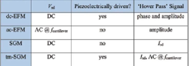
In the field of nanoelectronic devices, researchers have developed their own unique set of scanning probe imaging and manipulation techniques. In this article we review key techniques that allow for map-ping the distribution of electrical resistances, mea-suring local field-effect sensitivity, and engineering new electrical characteristics into nanoscale devices. Figure 1: (a) Schematic illustrating a carbon nanotube field-effect transistor and ‘hover pass’ (see text) microscopy geometries (not to scale). (b) AFM topography colored with electric force microscopy phase (Vtip = 8V, height = 20nm).
We use CNT devices as our working example, showing that parallely-connected CNTs can be individually analyzed, unwanted CNTs can be cut, and finally a point defect can be created which has single-molecule detection capabilities. While we focus on CNT devices, many of the same techniques are being used for nanowire4 and graphene5 devices. We first discuss how electric force microscopy (EFM) and scanning gate microscopy (SGM) techniques are used to characterize the electrical response of nanoelectronic devices. The information contained in EFM and SGM images is extremely valuable for relating the local electrical behavior of a device to the global device properties. In the specific example of our CNT network device, we use the knowledge of local resistance and local semiconducting behavior to choose the “best” CNT out of a mixture of parallel CNTs.
To acquire EFM and SGM signals, a conducting AFM probe hovers above an electrically contacted device (Figure 1a). During a “hover pass”, the mi-croscope maintains a constant separation between the conductive AFM tip and the surface (typical separations are 20 - 200nm). To achieve this con-stant separation distance, the microscope alternates between standard topographical line scans and hover pass line scans. A typical electrical contact configuration involves a current amplifier and three voltage sources (Vsd, Vtip, and Vbg). Depending on
the particular imaging technique, different voltage signals will be applied and the AFM tip may or may not be piezoelectrically driven (see Table 1).
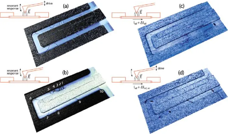
To demonstrate the utility of EFM and SGM, we used dc-EFM,6 ac-EFM,7 SGM,8 and tip modulated SGM (tm-SGM)9 to image a carbon nanotube (CNT) network device. The device is fabricated by growing CNTs on a SiO2/Si substrate (300nm oxide),10 and then patterning electrodes with photolithography. The images in Figure 1b and 2a Table 1: Key differences between modes used for imaging nanoelectronic devices.
are a combination of a dc-EFM data (color scale) and AFM topography. Many individual CNTs are seen bridging the gap between the source and drain electrodes. We are interested in learning which CNTs are metallic, which are semiconducting, which are well connected to the metal electrodes and which contain natural defects.
The electrostatic forces which give imaging contrast in dc-EFM6 (Figure 1b and 2a) are due to a voltage difference between the tip and the grounded elec-trodes. During each hover pass, the AFM cantilever is piezoelectrically driven at a fixed frequency (the fundamental resonance of the cantilever). If the AFM tip is above a grounded conductor, a vertical gradient in electrostatic force causes a shift in the resonance frequency of the cantilever. This reso-nant frequency shift modulates both the phase and amplitude of the cantilever motion. The dc-EFM image shown in Figure 2a allows us to quickly locate all conducting objects in the large (60μm) imaging area and requires minimal setup.
The vertical gradient in electrostatic force, which gives rise to the dc-EFM signal, depends on the tip-sample capacitance and the tip-sample voltage difference. When the tip hovers above a large-area electrode, the vertical gradient in tip-sample capaci-tance is large. When the tip hovers over a small CNT, the vertical gradient in tip-sample capaci-tance is small. Thus, the EFM signal from CNTs is weaker than from the electrodes. There has been steady progress in mapping out the vertical gradient in tip-sample capacitance to allow more quantitative imaging of the potential difference between the tip and the sample.11,12
Figure 2b shows an ac-EFM7 image in which different voltage signals are sent to the source and drain electrodes, respectively. This type of ac-EFM scan is used to visualize the voltage profile along the length of electrically-biased CNTs. A similar measurement can be done with dc-EFM, however, the ac-EFM signal is cleaner (more discussion below). CNTs labeled 1-4 in Figure 2b exhibit a sharp voltage drop where they meet the inner electrode (the length of the CNT appears uniform black). This sudden voltage drop indicates a high contact resistance. The CNT labeled 5 exhibits a sharp voltage drop midway along its length. The location of the voltage drop corresponds to a sharp
bend in the CNT, showing that the bend is a point of high resistance. CNTs labeled 6-10 show a gradual voltage gradient along their length, indicat-ing that these CNTs are well connected to both electrodes, and are free from major electrical defects. These CNTs with small contact resistance will be subsequently singled out for additional engineering and experiments.
To obtain the ac-EFM signal in Figure 2b, an AC bias was applied to the outer electrode (frequency matching the cantilever’s mechanical resonance) while the inner electrode and the AFM tip were grounded. During the hover pass the cantilever is not piezoelectrically driven, instead cantilever oscil-lations are driven by capacitive coupling to the AC biased electrode. These oscillations are detected by monitoring the cantilever deflection signal using a lock-in amplifier. The oscillation amplitude is plotted as a function of tip position to create the ac-EFM image. Cantilever oscillations are strongest when the probe is near the biased electrode. The ac-EFM signal is “cleaner” than dc-EFM signals
because stray DC signals (such as charge on the insulating substrate) are invisible in ac-EFM. We now turn our attention to scanning gate techniques, which allow researchers to further characterize the electronic properties of individual CNTs. Scanning gate techniques identify the local semiconducting response of a nanoscale conductor, revealing the presence of localized semiconducting ‘hotspots’ and bottlenecks for electron transport.8 Figure 2c shows an SGM image, where the AFM probe acts as a roaming gate electrode to modulate the doping in the underlying electronics. The SGM image (Figure 2c) shows a single feature, indicating that the global semiconductor response of the device is dominated by a single CNT (labeled 10 in Figure 2b). Other CNTs are present in the imaging area, but the SGM signals from these are significantly smaller. Methods to improve sensitivity are discussed below.
The imaging contrast in Figure 2c corresponds to changes in global device current when the biased
Figure 2: ‘Hover pass’ microscopy data of a typical CNT FET. (a) EFM (Vsd = 20mV, Vbg = 0V, Vtip = 5 V, height = 20nm). Color scale
shows phase of cantilever response. (b) Alternating current EFM (Vsd = 100mV @ 63 kHz, Vbg = 0V, Vtip = 2V, height = 20nm).
Color scale shows amplitude of cantilever response. (c) SGM (Vsd = 20mV, Vbg = 0V, Vtip = 5V, height = 20nm). Color scale shows
the change in current, ΔIsd, through the device. (d) Tip-modulated SGM (Vsd = 20mV, Vbg = 0V, Vtip = 5V, height = 20nm). Color
probe locally changes the doping level in the under-lying electronics. A small source-drain voltage (Vsd)
is applied across the device to drive global current. By monitoring changes in current as a function of tip position, the local field-effect sensitivity can be mapped.
A variation of SGM which offers greater sensitivity is tip-modulated SGM (tm-SGM).9 Compared to conventional SGM, tm-SGM offers higher spatial resolution and is capable of resolving weaker sig-nals. Figure 2d shows a tm-SGM image. This scan reveals five CNTs with a semiconducting response (labeled 6-10 in Figure 2b). One CNT contains a region of highly localized semiconducting response, indicating the presence of a natural defect (labeled 8 in Figure 2b).
In tm-SGM the AFM cantilever is biased and piezoelectrically driven at its resonant frequency, resulting in an AC electric field which modulates the local doping level in the underlying electronics. The local field-effect response of the sample is mapped as a function of tip position by isolating the component of the conductance signal at the cantile-ver resonant frequency using a lock-in amplifier. The detailed characterization outlined in Figure 2 allows us to pick the best CNT out of the ten CNTs for building a nanotransistor with chemical
func-tionality. Using dc-EFM (Figure 2a), we identified the locations of all CNTs in a large area scan, pro-viding a road map for engineering. With ac-EFM (Figure 2b) we identified desirable CNTs with low contact resistance (no sudden drop in voltage at metal-CNT contact) and an absence of natural defects (no sudden drop in voltage along length of CNT). Finally, using SGM methods (Figures 2c and 2d), we identified CNTs with a semiconduct-ing response. The most desirable CNT for buildsemiconduct-ing a nanotransistor is one with low contact resistance, no natural defects, and a uniform semiconducting response along its length. The CNT labeled 10 in Figure 2b satisfies these criteria, and is singled out for further experimentation.
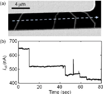
With initial characterization complete, we move to AFM manipulation techniques. Once a desired CNT is identified, we use AFM engineering to prune unwanted CNTs,13 then engineer an atomic-sized transistor element into the one remaining CNT.14 These techniques combine AFM lithogra-phy modes with control of the tip-sample voltage. Mechanical manipulation by AFM has also been used by many authors,15,16 but is not discussed here. To cut unwanted CNTs, a Pt-coated AFM probe is biased to Vtip = -10V, engaged with the surface, and
then dragged through the CNTs in contact mode (contact force ~ 6-9nN). Previously obtained dc-EFM and ac-dc-EFM scans, such as in Figures 2a and 2b, provide a convenient road map of the locations of the unwanted CNTs. Figure 3 shows a time trace of global device conductance during electrical cutting. Sharp decreases in device conductance are observed as the CNTs are severed. Afterward, ac-EFM and SGM scans may be used to verify that a single CNT forms the only electrical contact between the electrodes.
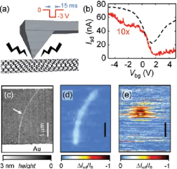
A single CNT can be converted into a transistor by further AFM-based engineering. Such nanotransistors approach the ultimate limit of miniaturization. To engineer an atomic-sized transistor, a conducting AFM probe is brought into gentle contact with the CNT and a -3 V, 15 ms square wave pulse is applied to the tip (Figure 4a). During the pulse, a chemical defect is incorpo-rated into the sidewall of the CNT, and the device’s electrical properties change significantly as a result (Figure 4b).14,17 Typical defects add between 10kΩ Figure 3: Electrical cutting of unwanted CNTs. (a) EFM
image of a device. Cutting path indicated by dotted arrow (Vsd = 25mV, Vbg = 0V, Vtip = 8V, height = 20nm). (b) Time
trace of cutting event (Vsd = 25mV, Vbg = 0V, Vtip = -8V,
to 1MΩ to the overall resistance of the circuit, and change the field-effect sensitivity of the device. Figure 4c shows a single-CNT device produced by the electrical ‘nicking’ method described above. SGM measurements show that the pristine CNT is uniformly gate sensitive (Figure 4d). Figure 4e shows an identical measurement following defect engineering where gate sensitivity is localized to the region around the defect. The SGM scan reveals that the defect acts as a gate sensitive bottleneck for transport, and the remainder of the CNT serves only as contact electrodes to the miniature transistor. A unique attribute of point-defect nanotransistors is their sensitivity to electrostatic potential within a very small detection volume. As such, they are ideally suited for single-molecule sensing applica-tions. Recently, point-defect nanotransistor sensors have been used to study biochemical reactions at the single molecule level.18,19
Figure 5 demonstrates the use of an AFM- engineered point-defect nanotransistor as a single-molecule sensor. The reaction between
N-(3-Dimethylaminopropyl)-N′-ethylcarbodiimide
(EDC) and a carboxyl group is used as a model reaction. EDC is frequently used to activate carboxyl groups in bioconjugation chemistry, and reacts reversibly with a carboxyl point defect on the CNT sidewall. The point-defect nanotransistor was immersed in an electrolyte solution containing EDC (Figure 5a). Figures 5b and 5c show the conductance data for a point-defect CNT before and after the addition of 20μM EDC, respectively. Discrete switching events are observed in the presence of EDC. This two-state telegraph noise is believed to reflect changes in the electrostatic environment resulting from the reaction with single EDC molecules.18 When EDC is bound to the defect, current through the CNT is low. When EDC releases from the defect, current through the CNT is high.
Summary
Using CNT network sensors as our working example, we have reviewed AFM-based techniques which are used to study and engineer nanoelectronic devices. We have used dc-EFM and ac-EFM to identify the locations and resistances of individual CNTs that are electrically connected in parallel. Next, SGM and tm-SGM were used to reveal the semiconducting response of each CNT.
Figure 4: Defect engineering in a CNT FET. (a) Schematic illustrating defect engineering geometry. (b) Transistor characteristics before (dashed black) and after (solid red) defect creation. The red curve has been multiplied by 10 (Vsd = 25mV). (c) AFM topography of a CNT device. A defect
was engineered at the location indicated by an arrow. (d) SGM data of the device shown in (c) taken before and (e) after defect engineering (Vsd = 25mV, Vbg = 0V, Vtip = 8V,
height = 20nm). The color scale (ΔIsd /I0 ) indicates changes
in device current relative to the baseline value, I0 . In (d) and
(e) the values of I0 are 280nA and 7nA, respectively.
Figure 5: Single-molecule detection of EDC. (a) Schematic illustrating detection geometry. The liquid potential is controlled with a liquid-gate electrode biased to Vlg. (b) Isd
trace of a nanotransistor in MES buffer (pH 4.5, Vsd = 25mV,
Vlg = 250mV). (c) Isd trace of the same device following the
MFP-3D is a trademark of Asylum Research. 6310 Hollister Ave. Santa Barbara, CA 93117 voice: 805-696-6466 fax: 805-696-6444
toll free: 888-472-2795 [email protected] 3-2012
With the information available in these scans a single CNT with desirable properties was singled out for further experimentation. The unwanted CNTs were electrically cut with a biased AFM probe to leave a device containing a single CNT. An atomic-sized transistor with chemical
functionality was engineered in the remaining CNT using a voltage pulse from the AFM probe. This nanotransistor was then demonstrated to be a single molecule sensor sensitive to EDC in an aqueous environment. This multi-step measurement and manipulation process illustrates the power of AFM-based techniques to map out and control the properties of nanoelectronic devices.
Acknowledgements
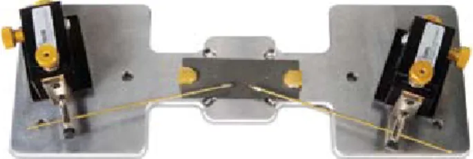
We thank Kristina Prisbrey for assistance with Figures 1, 4, and 5, and Bo Criss for assistance with Figure 2. We thank Sophie Ripp for initial experiments with EDC using suspended CNTs. We thank Paul Schuele and Sharp Labs of America for assistance with device fabrication. This work is funded by the Human Frontier Science Program. All AFM measurements and manipulations described here were performed with the MFP-3D AFM (Asylum Research, Santa Barbara, CA, www.asylumresearch.com) with the Probe Station Option (Figure 6).
References
1. S. S. P. Parkin, M. Hayashi, L. Thomas, Science 2008, 320, 190 -194.
2. A. Gruverman, Journal of Vacuum Science & Technology B:
Microelectronics and Nanometer Structures 1996, 14, 602.
3. G. A. Gibson, J. F. Smyth, S. Schultz, D. P. Kern, IEEE
Transactions on Magnetics 1991, 27, 5187-5189.
4. X. Zhou, S. A. Dayeh, D. Wang, E. T. Yu, Applied Physics
Letters 2007, 90, 233118.
5. R. Jalilian, L. A. Jauregui, G. Lopez, J. Tian, C. Roecker, M. M. Yazdanpanah, R. W. Cohn, I. Jovanovic, Y. P. Chen,
Nanotechnology 2011, 22, 295705.
6. Y. Martin, D. W. Abraham, H. K. Wickramasinghe,
Applied Physics Letters 1988, 52, 1103.
7. A. Bachtold, M. S. Fuhrer, S. Plyasunov, M. Forero, E. H. Anderson, A. Zettl, P. L. McEuen, Phys. Rev. Lett. 2000, 84, 6082.
8. S. J. Tans, C. Dekker, Nature 2000, 404, 834-835. 9. N. R. Wilson, D. H. Cobden, Nano Letters 2008, 8,
2161-2165.
10. J. Kong, H. T. Soh, A. M. Cassell, C. F. Quate, H. Dai, Nature 1998, 395, 878-881.
11. C. H. Lei, A. Das, M. Elliott, J. E. Macdonald,
Nanotechnology 2004, 15, 627-634.
12. M. Yan, G. H. Bernstein, Surface and Interface Analysis 2007, 39, 354-358.
13. J.-Y. Park, Y. Yaish, M. Brink, S. Rosenblatt, P. L. McEuen,
Applied Physics Letters 2002, 80, 4446-4448.
14. J.-Y. Park, Applied Physics Letters 2007, 90, 023112-3. 15. T. Junno, K. Deppert, L. Montelius, L. Samuelson,
Applied Physics Letters 1995, 66, 3627.
16. H. W. C. Postma, T. Teepen, Z. Yao, M. Grifoni, C. Dekker, Science 2001, 293, 76 -79.
17. D.-H. Kim, J.-Y. Koo, J.-J. Kim, Phys. Rev. B 2003, 68, 113406.
18. B. R. Goldsmith, J. G. Coroneus, A. A. Kane, G. A. Weiss, P. G. Collins, Nano Letters 2008, 8, 189-194.
19. S. Sorgenfrei, C.-yang Chiu, R. L. Gonzalez, Y.-J. Yu, P. Kim, C. Nuckolls, K. L. Shepard, Nature Nano 2011, 6, 126-132.
Figure 6: The Probe Station attaches to the MFP-3D scanner and allows easy electrical probing of sample properties, electrical biasing, and other measurements while the sample is being scanned with the AFM. A variety of electrical connections can be made and combined with various imaging modes.