ABSTRACT
HU, JIANCHEN. System-level Pathfinding Flow for Three Dimensional Integrated Circuits. (Under the direction of Dr. W. Rhett Davis).
The limited performance improvement of transistors in ultra-deep-submicron
technologies is making it more difficult to achieve computing performance increases from
scaling alone. Solutions to address this challenge come from combined system-level and
physical-level optimizations. At the system-level, more complex on-chip systems are
implemented by integrating various processing elements with interconnections to increase
parallel processing capability without the need to push transistors to high operating
frequencies or advanced technologies. At the physical-level, three dimensional integrated
circuits (3D-ICs) increase chip density and reduce wire delay by stacking multiple ICs
vertically with through-silicon-vias (TSVs). Both techniques enlarge the system design space
by introducing more design parameters such as the number of processing elements and types,
interconnection topologies, IC stacking schemes, and heterogeneous technologies.
Furthermore, the design parameters at different levels of abstraction interact with each other,
which necessitates a system-level “pathfinding” design flow to evaluate the design
parameters fast at early design stage. However, most state-of-the-art pathfinding flows focus
on the register-transfer and gate levels of abstraction for system modeling and are hard to
integrate with tools that focus on the transaction and instruction levels. In this work, we
present a electronic system-level (ESL) pathfinding flow that integrates transaction-level and
physical-level evaluation by using ESL models and interfaces, allowing fast, physically
© Copyright 2014 Jianchen Hu
System-level Pathfinding Flow for Three Dimensional Integrated Circuit
by Jianchen Hu
A dissertation submitted to the Graduate Faculty of North Carolina State University
in partial fulfillment of the requirements for the degree of
Doctor of Philosophy
Computer Engineering
Raleigh, North Carolina
2014
APPROVED BY:
_______________________________ ______________________________
Dr. W. Rhett Davis Dr. Eric Rotenberg
Committee Chair
BIOGRAPHY
Jianchen Hu was born on 4th Sep. 1984 in Beijing, China. He received his Bachelor’s
degree in Electrical Engineering in Tsinghua University in 2007. In fall 2007, he began his
graduate studies in the Electrical and Computer Engineering Department in North Carolina
State University, Raleigh, NC. From June 2008, he has been working in the Methodologies
for User-friendly System-on-a-chip Experimentation (MUSE) group of Prof. Rhett Davis in
the field of network-on-chips in multiprocessor system issue.
From fall 2009, he works as a Ph.D student with Dr. Rhett Davis. His research
interests include transaction-level modeling, computer architectures and 3D specific EDA
ACKNOWLEDGMENTS
First I would like to express my love to my parents who support me through my studies
I would also like to thank my advisor Dr. Rhett Davis for the great Ph.D research
experience offered. He always guides me for my research work and supervises me with his
knowledge, cutting-edge idea and enthusiasm of research.
I would like to thank Dr. Eric Rotenberg, Dr. Greg Byrd and Dr. Gregory Reeves who
serve me as my committee members.
Special thanks to Shivam Priyadarshi who work with me and help me a lot with my
research work in detail
I would like to thank all my colleagues and friends at North Carolina State University: Yi
Lou, Christopher Mineo, Zhuo Yan, Zhenqian Zhang, Wenxu Zhao, Harun Demircioglu, for
TABLE OF CONTENTS
LIST OF TABLES ... vii
LIST OF FIGURES ... viii
Chapter 1 Introduction ... 1
1.1 Motivation ... 1
1.2 Contribution ... 5
1.3 Organization ... 6
Chapter 2 Related Works ... 8
2.1 Introduction ... 8
2.2 Network-on-Chip Introduction and Design Space ... 10
2.3 Transaction-level Modeling ... 15
2.4 system-level CAD flow... 18
2.4.1 RTL-centric flow ... 18
2.4.2 TLM-centric flow... 20
2.5 Thermal Analysis tools ... 24
2.6 Summary ... 24
Chapter 3 System-level Pathfinding Flow ... 26
3.1 Introduction ... 26
3.2 Pathfinding Flow Descriptions ... 28
3.2.1 Overview ... 28
3.2.2 Front-end Part Description ... 31
3.2.3 Back-end Description... 32
3.3 Transaction-level Simulation with GEMS framework ... 40
3.3.1 Event-driven Simulation ... 40
3.3.2 Adding Interconnect Model ... 42
3.4 Summary ... 44
Chapter 4 High-level Power Model and Characterization ... 46
4.1 Introduction ... 46
4.2 Current High-level Power Model... 48
4.2.1 CACTI, the cache & memory model ... 48
4.2.2 ORION: On-chip router power model ... 50
4.2.3 McPat: Processor power model ... 50
4.3 Power Model Characterization Flow ... 51
4.4 Power Model Characterization for crossbar used in on-chip router ... 54
4.4.1 Crossbar design description ... 55
4.4.2 testbench generation and characterization ... 57
4.4.3 Result Analysis and Comparison with Orion 2.0... 61
4.5 Summary ... 66
Chapter 5 Physical-level Analysis ... 67
5.1 Introduction ... 67
5.2 ESL Floorplan based physical analysis framework ... 70
5.3.1 Global routing introduction... 72
5.3.2 Graph Model and Routing Algorithms ... 73
5.3.3 Adjusted Hadlock Algorithm for 3D global routing ... 76
5.3.4 Power estimation for global wires ... 78
5.4 Summary ... 78
Chapter 6 Case Study ... 80
6.1 Introduction ... 80
6.2 Multi-core case... 81
6.2.1 System Overview ... 81
6.2.2 Core Model Integration and Multiprogram Support ... 83
6.2.3 Core and Cache Power Estimation ... 86
6.2.4 Transaction-level simulation result ... 87
6.2.5 Physical-level simulation result ... 89
6.3 NoC test case... 94
6.3.1 System Overview ... 95
6.3.2 Core and Interconnect Power Estimation ... 100
6.3.3 Transaction-level simulation result & analysis ... 101
6.3.4 Physical-level simulation result & analysis ... 105
6.4 Summary ... 111
Chapter 7 Conclusion ... 113
REFERENCES ... 115
APPENDICES ... 120
Appendix A Pathfinder3D ... 121
A.1 Design File Format... 121
A 1.2 Stimulus File Format ... 123
LIST OF TABLES
Table 4.1 High-performance and low-power configurations for caches in CACTI 6.5 ... 49
Table 4.2 Design and characterization parameters for crossbar power characterization ... 61
Table 6.1 Core power consumption for each stage ... 86
Table 6.2 Cache model parameters for power and area estimation in CACTI ... 87
Table 6.3 L2 miss rate of quad-core system running MCF and BZIP benchmark with different L2 size ... 88
Table 6.4 2D and 3D temperature and global wire analysis result for quad-core case with (a) 256KB and (b) 1024KB L2 bank ... 92
Table 6.5 Power and area estimation for elements used in NoC case ... 101
LIST OF FIGURES
Figure 2.1 Circuit-switching Scheme ... 11
Figure 2.2 Two types of topologies for NoCs. (a) Mesh and (b) Flattened butterfly ... 13
Figure 2.3 NoC with Ring topology ... 14
Figure 2.4 Pathfinding flow presented in Rako’s work ... 17
Figure 2.5 Physical-analysis flow used in SpyGlass3D ... 19
Figure 2.6 TLM-2.0 Architecture ... 22
Figure 3.1 System-level Evaluation Flow for 3D-IC ... 30
Figure 3.2 Cross section of the first three tiers of the FreePDK3D45 technology. ... 34
Figure 3.3 Block communication with event-driven simulator ... 42
Figure 3.4 Example to add interconnections to GEMS framework... 44
Figure 4.1 High-level Power Model Characterization Flow ... 53
Figure 4.2 Schematic of Logic Gate Based Crossbar ... 57
Figure 4.3 Test Bench Generation Flow ... 60
Figure 4.4 Characterization result for 7-port crossbar with 3 different data input pattern ... 62
Figure 4.5 Characterization result for 7-port crossbar with time and port dependent request pattern . 63 Figure 4.6 Power model format for 7-port 16-bit corssbar ... 64
Figure 4.7 Power estimation of crossbar from Orion 2.0 ... 65
Figure 5.1 Physical-level analysis scope ... 69
Figure 5.2 Pathfinder3D: ESL floorplan-based analysis engine ... 71
Figure 5.3 Global routing and detailed routing scheme ... 73
Figure 5.4 Different graph model. (a) Actual layout (b) Grid model (c) Checker Board model and (d) Channel intersection model ... 75
Figure 5.5 Pseudo code fro adjusted Hadlock algorithm for global routing in 3D-IC ... 77
Figure 6.1 Quad-core test case ... 82
Figure 6.2 Attaching detailed core model to TLM simulation framework ... 84
Figure 6.3 Simple TLB for address conversion ... 85
Figure 6.7 Wire length distribution comparison between 2D and 3D floorplan for (a) 256KB L2 bank
and (b) 1024KB L2 bank ... 93
Figure 6.8 Router architecture for packet-switched based network ... 96
Figure 6.9 Parallel transactions in Ring topology ... 97
Figure 6.10 (a) 8X8 Mesh topology and (b) 4X4X4 Mesh topology ... 99
Figure 6.11 Pareto-efficiency fro 64-node NoCs ... 104
Figure 6.12 Power efficiency of a 64-node NoC with different 3D partitioning... 105
Figure 6.13 Temperature distribution for 4X4X4 Mesh topology ... 106
Figure 6.14 Global wire distribution comparison between 8X8 and 4X4X4 Mesh NoCs ... 107
Figure 6.15 Global wire distribution of 4X4X4 Mesh NoC for 1-tier and 4-tier cases ... 108
Figure 6.16 Pareto-efficiency for 64-node NoC with temperature limiation ... 110
Figure 6.17 Pareto-efficiency for 64-node NoC with global wire length limitation ... 111
Figure A.1 Design file format of Pathfinder3D ... 122
Figure A.2 Stimulus File Format in Pathfinder 3D ... 123
Chapter 1
Introduction
1.1 Motivation
The limited performance improvement of transistors in ultra-deep-submicron
technologies is making it more difficult to achieve computing performance increases from
scaling alone [1]. As the size of transistors shrink, the delay and power consumption are not
scaled down at a pace of Moore’s Law. This situation is further aggravated by the growing
complexity of interconnects. The average length of global wires is determined by chip size
and tends to remain fixed as technology scales, but the delay of a unit length wire is rising [2].
Meanwhile, the increasing on-chip system complexity coming from high chip integration
with advanced technology nodes raises the manufacturing cost due to lithography and
patterning integration [3]. The chip yield and variation in electric characteristics of transistors
further increase cost for advanced technologies. Furthermore, the slowdown in supply
voltage scaling makes it more difficult to reduce power consumption.
To address these challenges, new techniques at both system-level and process-level are
solution has been accepted as commercial offerings today [4] [5]. Chip multiprocessors also
get the benefit of heterogeneity by applying mixed type (fast/slow hybrid) of cores to run
different applications [6]. To further increase parallel processing ability and meet the
requirement of on-chip communication, network-on-chip (NoC) architectures allow
integrating more processing elements (generic cores, DSP processors or other dedicate
function units) on a single chip with network interconnections [7]. An NoC is considered a
scalable architecture since the interconnections with different topologies distribute on-chip
traffic contentions and congestions compared to shared-bus-based interconnections.
Moreover, the regularity of NoC structure makes it easy to extend the number of on-chip
cores by repeating the same unit architecture [8].
At the manufacturing process-level, three dimensional integrated circuits (3DIC) address
some of these challenges by stacking different ICs vertically [9], [10]. Circuits in different
tiers of a 3DIC can communicate with each other through different types of Through Silicon
Vias (TSVs), which can largely reduce the total wire length and routing congestion compared
to a conventional 2D implementation [11], [12]. The reduction of global wire length results
in power and delay reduction of interconnections. Another benefit from 3D integration is
high memory bandwidth by building on-chip memories and connecting with cores by using
TSVs. In that sense the conventional off-chip latency between cores and memories is
converted to on-chip latency between tiers, and wide core-to-memory interfaces can be
implemented within the TSV capacity [13]. Since tiers can be manufactured independently in
different technologies, it gives flexibility to optimize the design by evaluating different
wire lengths can be reduced, leading to cost reductions from reduced metallization layers,
and heterogeneous integration can reduce the cost by implementing non-critical components
in cheap technologies [15].
Both CMP/NoC architecture and 3D integration provide a rich variety of choices to
system designers at both the architecture-level (core types, on-chip cache size, network
topologies) and the physical-level (homogenous vs. heterogeneous partitioning of a design,
number of stacking layers in 3D design, integration of heterogeneous technologies, and
different types of 3D bonding methods). In [16], an NoC architecture is applied with 3D
integration to get both benefits from architectures and 3D integration. However, the large
system design space necessitates a huge amount of effort to model the system and identify its
critical parameters. In such cases, it is necessary to develop system-level computer-aided
design (CAD) flows that help designers to evaluate various designs and make the best design
decisions.
The CAD flows for system-level design and evaluation can be divided into two
categories: register transfer-level (RTL) centric and electronic system-level (ESL) centric
flow. The RTL centric flow evaluates designs based on detailed gate netlists, generating
accurate estimates of power, area and other metrics. It is usually used by designers to verify
and optimize a design at the circuit implementation phase. The detailed netlist requirement
does not help much for making architectural decisions. On the other side, the ESL centric
designs since both benefits (wire reduction, heterogeneous technologies, etc.) and costs
(temperature rise, TSV impact) are tightly dependent on physical-level parameters. Fast
evaluation of the impact of physical decisions on ESL behavior is required to effectively
explore the rapidly expanding design space. The term “pathfinding” is used for this kind of
approach. The pathfinding flow integrates system-level behavior and physical-level analysis
while providing useful feedback for computer architects and valuable input for circuit
designers, targeting different communities with the intent to close the gap between high-level
design evaluation and circuit-level design implementation. In this work, we present a
pathfinding flow that integrates TLM simulator and ESL physical analysis tools to allow fast
system designs evaluation with the impact of physical-level metrics such as temperature and
global wires.
A necessary part of any pathfinding flow is the power model. Accurate power estimation
is critical for ESL performance evaluation. Furthermore, ESL power-estimates are tightly
coupled to physical-level temperature analysis, due to the exponential dependence of leakage
power on temperature. There are two types of power models: characterized models and
analytical models. Analytical models predict block power based on estimated capacitance by
using the assumption of certain circuit structures. They are often integrated within ESL
centric flow to provide fast power estimation. However, as more physical-level factors are
taken into account in analytical power models, the task of fitting model parameters becomes
more difficult, and users tend to find their estimates diverging more and more from actual
implementations. Characterized models predict power by breaking designs into standard cells,
accurate power number but requires RTL design to be able to characterize the power. In this
work, we characterize power to obtain a higher level, abstract power model for the ESL
simulator, so that the RTL and gate levels can be avoided with minimum reduction in
accuracy.
1.2 Contribution
Our main contribution in this work is to develop a pathfinding flow for fast evaluation at
system-level with the consideration of physical-level impact in 3D-ICs. The flow integrates
transaction-level simulation to capture run-time dependent system behavior and physically
aware analysis to estimate temperature and global routing result. The transaction-level
simulation framework allows user to build various systems, exploring design space in terms
of architectural configurations. An open-source ESL framework named Pathfinder3D [17] is
developed for physical-level analysis used in our pathfinding flow. This framework provides
convenient method to examine the impact of 3DIC manufacturing options such as stacking
schemes and wafer technologies. Furthermore, it sets up an ESL floorplan based prototype
which bypasses the requirement of detailed gate netlist and makes it easy to map the
high-level system description to physical-high-level. A set of physical-high-level tools are built around this
prototype for thermal and global routing analysis. By using this pathfinding flow, users can
easily evaluate the benefits of 3D technologies without the detailed design, and compare
Another contribution in this work is the power model characterization flow. Analytical
model used to be considered an easy-to-use and scalable approach for power estimation.
However, as technologies keep advancing, more physical/technology parameters are needed
to be considered to perform power analysis which makes analytical power model hard to
build and use at system-level. In this work, a characterization flow is presented for power
model generation. We incorporate standard cell power estimation flow to get accurate
dynamic and static power number by using gate level library but characterize the power
model at ESL. It is a fast approach to read transaction-level simulation output and provide
power number back feedback to high-level analysis as well as physical-level analysis such as
temperature estimation. The one-time building effort to characterization is paid off once the
power model is set up and been used by various systems.
1.3 Organization
We organize the work as follows. Chapter 2 reviews various RTL-centric and
ESL-centric CAD flow. In chapter 3, the pathfinding flow is presented in detail, describing how
we build system at high-level and generate information for physical-level analysis.
Meanwhile, the thermal analysis tool that is used in this work to get temperature analysis
result is introduced [18]. High-level power model characterization flow is presented in
chapter 4, which describes how we use transaction-level parameter to characterize power
based on detailed netlist. And we compare our characterized model to analytical model to
illustrate the necessity of characterization. In chapter 5, the floorplan based pathfinder3D
circuit design. And a global routing tool, it is presented to show how physical analysis can be
performed based on ESL floorplan rather than detailed gate-level netlist. Two case studies
are shown in chapter 6. The multi-core case shows how users examine 3D benefits for
different system configuration without detailed design. And the NoC case illustrates the
importance to have physically aware feature pathfinding flow to make architectural design
Chapter 2
Related Works
2.1 Introduction
Developing a CAD flow for system-level design exploration and evaluation becomes
more and more difficult due to the increasing system complexity and technologies shrinking.
Several key issues need to be addressed for system-level CAD flow. First, the CAD flow
needs to choose the right design parameters as well as performance metrics for evaluation.
Complex system contains hundreds of design parameters and it is impossible to capture all of
them before actually implementing the design with limited time and effort invested. Thus
picking critical sub-set of input parameters for system evaluation is important to reduce the
design effort in the follow-up design phases. Another important feature for the flow is to
capture the run-time dependent effect of a system. Power and performance of a system not
only depend on the hardware architectures but also applications [19] [20]. Identifying the
performance variation due to different applications helps system designers to make design
decisions and apply various optimizations [21]. The trade-off between modeling/simulating
effort and the accuracy of predicted performance needs to be considered in system-level
CAD flow, especially for complex system such as CMP or NoC. In that sense, selecting
result with fast simulation speed. In 3D-ICs, those challenges become more difficult for
system-level researchers and designers to evaluate and optimize designs. 3D integration with
multiple tiers and 3D floorplans make it more difficult to find out key design parameters. The
technology heterogeneity and different bonding/stacking schemes also need to be evaluated
with other system-level parameters. 3D integration also requires the flow to support more
dynamic features. For example, the temperature rise in 3D-ICs increases leakage power
consumption and leads to higher temperature, in that case a dynamic thermal analysis need to
be performed to figure out an appropriate thermal management method [22].
The system-level CAD flow can be divided into two categories: RTL-centric and
TLM-centric flow, focusing on different scopes and objectives. The RTL-TLM-centric flow targets
detailed design optimization. It predicts accurate performance estimation to reflect subtle
design changes by incorporating the commercial physical design flow. However, such an
approach requires detailed RTL design netlist as an input, which takes too much time to
generate for complex system evaluation. On the other hand, TLM-centric flow targets
system-level design space exploration for computer architects to compare complex systems
with large amount of architectural configurations. Modeling speed and the capability to
model large systems are considered to be the most important features in this kind of flow.
The divergent objectives make the two types of flow developed in parallel and used by
computer architects and circuit designers in their research scopes respectively.
physically aware analysis which is usually in RTL-centric flow to TLM-centric flow for fast
system-level evaluation is the solution to that problem. In this chapter, we first introduce the
basis of TLM simulation, and then the works of different types of CAD flows for
system-level evaluation.
2.2 Network-on-Chip Introduction and Design Space
As the number of processing cores increases in multi-core system, the conventional
bus-based or dedicated wire-bus-based on-chip interconnections cannot provide enough bandwidth
for the traffic among cores. To address the bottleneck of on-chip communication bandwidth,
Network-on-Chip (NoC) is implemented by connecting on-chip processing elements with
network structures. There are many factors that affect the network performance such as
routing and arbitration algorithms, network buffer size, router structures, etc. In this work,
we will examine two system-level parameters of NoCs: switching schemes and network
topologies.
NoCs can be divided into two categories according to the switching schemes:
packet-switched based NoCs and circuit-packet-switched based NoCs. Both of them brings the concept
from computer networks. A key feature of packet-switched based networks is that the
transactions can be stored and routed at network routers based on its destination information
and the routing algorithm. In a multi-hop network, transactions generally are not sent to the
destination node directly, but routed at each node independently. In that case, buffers are
required in each network node due to possible traffic contentions and congestions. This
without interactions can be routed and transmitted simultaneously. The parallel transactions
feature increases the bandwidth by improving the channel utilization. By implementing the
same router structure and routing algorithm for each network node, it’s easy to scale the NoC
to large number of nodes [36].
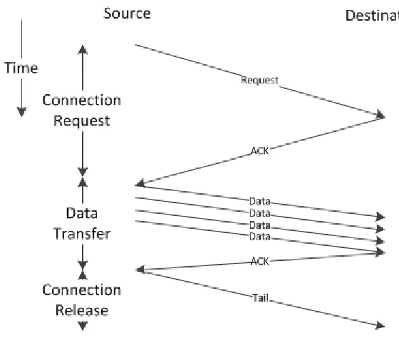
Different from packet-switched NoCs, circuit-switched based NoCs establish dedicated
“circuit” for data transfer between source and destination nodes which provide more
end-to-end features compared to packet-switched based NoCs. Typically data transfer in
circuit-switched networks can be divided into 3 phases: connection request phase, data transfer
phase, and connection release phase. Figure 2.1 shows the 3 phases switching scheme.
scheme. Once the destination node accepts the request, an acknowledgement (ACK) packet
would be sent back to the source node. The request and ACK packets reserve a dedicated
channel for following data packets so that other transactions cannot use the same channel.
The data transfer phase begins after the channel has been established. Multiple data packets
are sent out through the channel without the need of routing and storing in intermediate
nodes. After all data packets are sent out, the connection release phase starts with a tail
packet sent to the destination. Similar to connection request phase, the tail packet releases the
channel so that other transactions can use it. Compared to packet-switching, circuit-switching
does not require data buffers for each network node thus reduce area and power of the
network. Several implementations make use of these advantages to reduce the network cost
[37-39]. However, circuit-switching requires extra phase to establish and release channel
which reduces the effective bandwidth by introducing extra latency. And the time to setup
and release channel increases as the number of network nodes grows, making the
circuit-switched based NoCs hard to scale up.
The network topology represents the arrangement of the network nodes and the links
connecting them. We introduce several widely used topologies here for the case study we
used later in this work.
The first one is mesh topology. As fig. 2.2 (a) shows, mesh has regular shape and links
which make it easy to implement. However, the nodes in mesh topology can only connect to
the adjacent nodes which limits the performance. Once the mesh grows larger, nodes in the
center of the network need to process more traffic than the edge and corner ones. To solve
butterfly is introduced [40]. The main difference between mesh and flattened butterfly is
nodes in flattened butterfly topology have direct access to all the nodes in the same row and
column. As fig. 2.2 (b) shows, each node in a flattened butterfly topology has 6 ports
regardless of the locations. Such high-radix nodes greatly improve the bandwidth of NoC
since the maximum number of hops required for data transfer reduces from 6 to 2 compared
to mesh topology. However, such high-radix routers consume more power and area. And
increasing radix can also slow down the operating frequency. Moreover, only on-chip traffic
centric applications can utilize the extra possible bandwidth provided by flattened butterfly,
otherwise the bandwidth benefit is wasted due to not enough on-chip transactions.
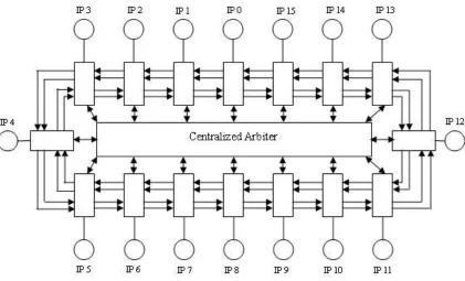
Figure 2.3 NoC with Ring topology
The third topology is a ring topology. Different from mesh and flattened butterfly, it is
usually used in circuit-switched based rather than packet-switched based ones. As fig. 2.3
shows, nodes in the ring topology connected with each other through a shared ring bus, and a
centralized arbiter controls all the transaction on the ring. Compared to other topologies, ring
topology has simple router architecture since no buffer and arbitration unit is needed. Since
buffers consume large percentage of router power, the ring topology helps reduce the power
as well as area [41]. However, ring topology has the worst scalability. Increasing the size of
2.3 Transaction-level Modeling
There are two critical aspects in hardware description and modeling: the notion of timing
and the connection between function blocks. Based on different modeling approaches of the
two aspects, we have two conventional modeling styles: RTL modeling and functional-level
modeling. RTL model specifies all details of port connections between logic blocks. Each pin
connection needs to be specified and the type of input/output need to match. In
functional-level model, there are usually no ports between blocks and data transfer is implemented by
using function calls. Timing in RTL is modeled in detail at cycle count. In contrast,
functional-level model does not hold any timing information.
Transaction-level is a level of abstraction in between the RTL and functional-level.
Transaction-level modeling is an approach to model digital systems where details of
communication among modules are separated from the details of the implementation of the
functional units or the communication architecture [23]. As such, TLMs usually do not
include pin-accurate detail like RTL models, but aggregate many input/output signals into
ports and channels. Communications among channels are implemented by calling functions.
Such approach avoids implementing detailed interfaces between block and simplifies data
transfer. TLMs also support two modeling styles in terms of timing annotation method:
loosely-timed and approximately-timed. Loosely-timed modeling style allows few timing
depend on simulation time strictly. Approximately-timed modeling provides more timing
points in a transaction. It breaks a transaction into several phases. The module could annotate
delay in each phase, which was implemented by using timeout or timed event notification.
Approximately-timed model supports pipelined structure implicitly.
The timing feature and simplified port declaration allows TLM to support hardware
modeling and simulation by using software-based environment such as C++ or SystemC.
Simulation environment and flexible timing annotation methods make TLMs can be set up
2.4 system-level CAD flow
2.4.1 RTL-centric flow
One RTL-centric pathfinding flow is presented in [25] as figure 2.4 shows. In that flow,
first different component models (typically adders, multipliers, muxes of different sizes and
datapath widths) are synthesized and performance parameters are extracted. Meanwhile, a
high-level C++ based system description is generated. Then a High-level Synthesis (HLS)
process translates the system description into completed RTL by using the performance
parameters. After that, the RTL netlist is synthesized to gate-level netlist via standard
physical design flow. In the end, a physical prototype is generated by using gate-level netlist.
The prototype is simplified from completed layout, but still keeps place and route
information as well as parasitic capacitances to estimate power, delay and area of the design.
The result feeds back to HLS phase and it will regenerate RTL netlist to optimize timing.
Such flow links physical-level analysis to system-level from two aspects. 1) The performance
extraction phase enables “technology aware netlist generation”. 2) The feedback from
physical prototype to HLS allows designers to optimize architectures based on physical-level
analysis result. However, the HLS process is highly restricted and the example shown in that
work only makes small part of their design in C. And the design parameters and performance
metrics are limited. The optimization focuses on operating frequency, area and power
consumption which are all “circuit-level” parameters, the run-time/simulation based
architectural-level parameters analysis prohibits the flow from being used by system architects.
The SpyGlass3D is another RTL-centric flow focusing on physical-level analysis of
3DIC as figure 2.5 shows [26]. This flow provides physical-level performance estimation and
optimization by extending standard 3D-IC design flow. The analysis starts with a 2D RTL
netlist and get initial floorplan by using typical 2D physical design flow. Then the blocks
which will move to another tier are marked as point objects, and floorplans in different tiers
are generated based on point objects. To specify the pad and TSV locations, a pad clustering
process is used to aggregate TSVs. Then another floorplan with specification of internal and
external pad information is generated. The physical-level analysis focuses on different
partitioning schemes and wire length optimization. It shows that good partition for 3DIC can
reduce the total wire length by 50% to get better power saving and cut off the maximum
length by 30% for better performance. As an evaluation flow, the work requires detailed
physical design netlist which makes it hard to use for system-level designers since it is hard
to integrate with other system-level tools due to the detail requirement.
2.4.2 TLM-centric flow
Different from RTL-centric flow, TLM-centric flow focuses on modeling complex
system at architectural-level. A toolset for multi-core system modeling and simulation named
GEMS is presented in [27]. It provides a framework to simulate multi-core with memory
hierarchies and coherent protocols. By including a texture description of cache protocols,
users can easily build multi-core systems with different cache structures to compare the
system performance. There are two major contributions that make GEMS popular. First, it
system-level configuration such as number of cores, caches, cache hierarchy system-levels and cache-to-core
connection configurations can be modified without coding work but only texture
specification. That allows computer architects to explore large design space fast and easily.
Second, GEMS provides good timing estimation across the system, the latency of each
transaction can be simulated in detail due to the time scheduler. We consider GEMS as a
transaction-level simulator according to these important features above. Since GEMS focuses
on cache hierarchies only, a CPU simulator called M5 is integrated which provides features
that many CPU-centric simulators lack, such as full-system (including OS) simulation and
I/O support [28]. The combined simulator GEM5 enlarges the simulator scope [29]. Setting
up and simulating a system in GEM5 is nothing more than writing a python script that
instantiates and connects various components with each other. Some other tools targeting
peripheries in CMP scope are integrated into GEMS-GEM5 framework. For example, a
cycle-accurate memory simulator is integrated to provide accurate memory latency [35]. One
of the GEMS-GEM5 framework limitations is the framework targets CPU-centric system
only such as multi-core or many-core with various cache hierarchies, but not for generic
SoCs which also require system-level simulation for design space exploration. It is easy to
add new cores and caches, but the core-cache backbone is hardly changeable. And there is no
built-in support for physical-level analysis such as area and temperature.
SystemC is another TLM framework [30]. It was created largely in response to the need
simulation kernel. This kernel works with events and processes in an abstract manner,
coordinating events and switching between processes, thereby allowing SystemC to simulate
the implicitly parallel hardware features. Modules and processes describe the abstraction of
structural information, while interfaces and channels represent the abstraction for
communications. Data is transferred between modules through interfaces and channels. Since
SystemC is built on top of C++, all the C++ features can be implemented to speed up
modeling and increase code reusability.
To further help establishing a transaction-level model based system, a standard for
transaction-level modeling with SystemC is presented in TLM-2.0 standard [31]. Fig 2.6
shows the architecture of TLM-2.0. There are several key contributions in TLM-2.0 to help
standardize transaction-level modeling. First one is the standard transaction class
generic_payload. As the name implies, this transaction class defines a data structure for
communications between function blocks. It contains basic information for data transfer such
as command type, address, ID, data pointer as well as an extension class to specify custom
attributes. TLM-2.0 also defines sockets which are not only aggregations of signals and ports
but also interfaces and transaction methods. Each module with appropriate type of socket
could bind with each other by using port-export binding method, and sends transactions by
calling the relative method of the socket. Implementing sockets further reduce the bonding
effort between blocks when designers try to build or modify the top level module of large
systems. To model a variety of bus standards which are used in most of the SoCs, TLM-2.0
introduces a base protocol. The base protocol specifies a set of rules regarding to data
transfer such as transaction phases and transaction statuses. By using (part of) the protocol
feature, it is easy to model different bus protocols without requiring specific extensions.
TLM-2.0 standard reduces modeling effort by aggregating ports, signals, data structures to a
higher level of abstraction and help designers to build large complex systems by reusing
codes from other sources. However, the systemC platform is still focusing on
2.5 Thermal Analysis tools
Both of the TLM-centric flows mentioned above are lacking of physical-level analysis. A
thermal analysis tool called HotSpot [32] is used by system-level designers to estimate
temperature. Building the thermal model at ESL, HotSpot takes a transient power trace as
input for which it typically relies on an external detailed cycle-accurate performance/power
simulator. The detailed architectural simulation approach works well if only the processor
alone is considered, but this approach is not feasible for simulation of System-on-chip (SoC)
containing several processors, memory and bus, etc. in realistic simulation time. To explore
the impact of 3DIC, HotSpot is extended later in [33]. However, it has several 3D specific
limitations. For example, currently it does not explicitly support modeling of TSVs and
microbumps [34].
2.6 Summary
In this chapter, we discussed the challenges to create CAD flow for system-level design
exploration and evaluation. The complex system and 3DIC technologies add more difficulties
at both architectural-level and physical-level. Large amount of architectural configurations,
run-time dependent requirements, different 3D integration schemes and limited
modeling/simulation time budget make conventional CAD flows hard to capture all the
necessary parameters and metrics for complex systems.
There are two types of system-level CAD flows: RTL-centric and TLM-centric flow. The
physical-level analysis such as area estimation and wire length and distribution estimation.
The objective of RTL-centric flows is design optimization at circuit-level, targeting at circuit
designers and manufacturers. On the other hand, the TLM-centric flows focus on complex
system modeling which captures application dependent parameters as well as architectural
parameters. The objective of the TLM-centric flows is to evaluate large amount of
architectures with minimum effort and allow computer architects to find out the best design
at an early stage. RTL-centric flow is hard to use by computer architects due to the huge
effort to build detailed design before the evaluation. TLM-centric flow does not contain
physical-aware feature which makes it hard to detect the impact of physical-level parameters
especially in 3DIC. Due to the challenges of system-level design with 3DIC, integrating
Chapter 3
System-level Pathfinding Flow
3.1 Introduction
3D integration enlarges the system-level design space by adding more physical-level
choices such as number of stacking tiers, heterogeneous technologies for different tiers, and
different 3D bonding methods. Those physical-level choices affect the system-level design
decisions and necessitate a system-level physically aware pathfinding flow. Such a flow
should be able to evaluate systems at physical-level without the need of detailed gate netlist.
To be specific, an system-level pathfinding flow for 3DIC should be able to (a) explore
design spaces at appropriate level of abstractions for different 3D related physical parameters
such as stacking schemes, floorplans and wafer technologies. And (b) shows the feedback
added by physical choices and help system designer to optimize the design. Furthermore, the
pathfinding flow should provide valuable input for circuit designer or manufacturer to guide
their work.
Current pathfinding flows for 3D-IC evaluation have several problems. Firstly, the
physical-level pathfinding flow requires too much design details. For example, in [25] a
completely RTL netlist is required to perform the simplified physical design flow to get
simulation. Then the power data can be used for temperature or power distribution analysis.
In [26], a completely gate-level netlist is required to explore different partitioning and
floorplanning schemes. These approaches require huge effort to perform system-level
analysis and prevent computer architects to evaluate their designs in architectural-level.
Secondly, the system-level pathfinding flow is lacking of flexibility to build various systems.
For example, in [27] people can easily build a multi-core system with the built-in feature
such as memory hierarchy and scheduler. However, it is extremely difficult to add different
modules or features since it usually requires hard-coded and time consuming. Thirdly, most
of the pathfinding flows are lacking of integration of architectural-level and physical-level
analysis tools. Lots of physical-level analysis tools start from RTL or gate-level design netlist,
which is hard to obtain from system-level CAD flow. On the other side, system-level CAD
flow does not provide enough area, power and floorplanning information to perform
physical-level analysis. The difficulty of integrating system-level and physical-level analysis
together prevents architectural and physical level co-optimization for complex system at
early design stage, which is more and more important due to the time-to-market pressure and
coupled design space in 3D-ICs.
In this chapter, we present a pathfinding flow for fast system-level 3D-IC evaluation. Due
to the complexity of 3D systems, the entire pathfinding flow is based on ESL instead of RTL,
yet still provides enough physical-level analysis to evaluate the impact of 3D integration. The
pathfinding flow we presented here can build and evaluation system fast while providing
useful information about power, performance and physical-level metric such as temperature
for system designers.
3.2 Pathfinding Flow Descriptions
3.2.1 Overview
Fig. 3.1 shows the proposed pathfinding flow, which is divided into two parts: the
front-end part and the back-front-end part. In the front-front-end part, an ESL system description is created to
evaluate system performance and provide input to the back-end part. To capture the dynamic
effects of underlying application on power and performance, a transaction-level simulator is
implemented. The simulator can show the performance in terms of number of transactions
per cycle for each IP block by running a benchmark. Furthermore, a high-level power model
is used to calculate the dynamic and static power based on IP configurations and performance
results from a TLM simulation. The back-end part of the flow starts with an ESL floorplan
obtained from system level description using an area model of components. Users must
specify technology information of each layer/tier of the stack (the “wafer technologies”),
information about TSV-based stacking of different tiers (a “stack technology”) and material
properties. To speed-up the thermal simulation, layers in the wafer technologies are collapsed
into a reduced set of layers, called composite layers. We feed the composite layers, rough
floorplan and power information to our in-house thermal simulator to generate the static and
wires connected between blocks, and TSVs for 3D integration. The routing tool generates
global wire length and distribution as well as total number of TSVs, which represent the cost
for actual implementation of the designs. The system description can be easily changed based
on obtained power, performance and thermal results and new iteration can be performed.
This flow facilitates fast design space exploration to find optimal 3D design without doing
3.2.2 Front-end Part Description
The frond-end part of the flow consists of a system description, a transaction-level
simulation framework, and a high-level power model to calculate power based on TLM
simulation results.
A. System description
As a first step, designers are required to create high-level system description for a set of
design parameters using functional and timing models of component IP blocks. This step
includes two phases namely: IP configuration and logical partitioning. In the IP configuration
phase, designer set appropriate parameters for each IP block (core type, cache size, etc.) and
in the logical partition phase, designer specifies how the IP blocks are connected to each
other and how the data is transferred among the blocks. If the system has caches and
memories, the cache policy and cache protocol are also determined in this phase.
B. Transaction-level simulator
It is important to capture the dynamic effects of underlying application on power and
performance; hence a transaction-level simulator is used. TLM based simulation can greatly
reduce the simulation time compared to RTL simulation with acceptable timing accuracy
all the blocks. Each block can schedule an event for the subsequent block. The global event
queue triggers all the appropriate events scheduled for current cycle. To ensure functional
and timing correctness, all the outputs of a block are available to other blocks in the next
cycle. Thus all the blocks can be triggered out-of-order. We get switching activity results
from this event-driven simulator in terms of cycle counts to estimate dynamic power.
C. Power Model
A high-level power model is needed for estimating power consumption. Computer
architects typically use analytical models to predict power. However, it can be difficult to
tune these models to accurately represent the expected power of a block after it has passed
through a physical design flow. We therefore chose to characterize the blocks by extracting
power models after carrying them through a complete physical design flow. This process is
time consuming, but it is faster than the alternative, which is to assemble the complete
system RTL before beginning a pathfinding study. By characterizing sub-blocks, we avoid
the effort of designing glue-logic and modifying block interfaces such that they are
compatible. The power model will be introduced in detail in Chapter 4.
3.2.3 Back-end Description
The backend of the proposed flow primarily consists of composite model extraction, ESL
floorplanning thermal and global routing simulation. It takes material properties, wafer and
stacking technologies descriptions as inputs. These data can be obtained from vendor PDKs.
vendor kits, we developed a free, open-source design kit compiler for stacked dies in a
predictive 45nm technology, which we call the FreePDK3D45 [43]. The kit represents a
five-tier stack of FreePDK45 predictive technology allowing the designers to maintain a complete
3D conception of their design. The kit supports three kinds of through-silicon-vias (TSV): a)
down via b) up via and c) through-tier via, as illustrated in Figure 3. The kit is intended for
use in demonstrating and debugging new OpenAccess-based design tools for 3DICs. As such,
the kit contains the basics of what is needed to perform schematic entry, SPICE simulation,
layout, DRC, and LVS checks.
Using FreePDK3D45 as an underlying framework, we have a developed an open source
toolset to deliver the path-finding flow proposed here [17]. The tool currently supports
thermal evaluation of TSV-enabled digital architectures as well as global routing analysis.
Here we describe composite-model extraction, rough floorplanning, thermal analysis and
routing aspects of the flow.
A Composited Model Extraction
Pathfinder3D’s technology-file format allows the specification of a new heterogeneous
3D stack with changes to only a few lines of code [17]. The materials section allows
specifying a list of material names, their thermal conductivities, densities and specific heat
capacities. Single-wafer manufacturing technologies and their associated layers, materials,
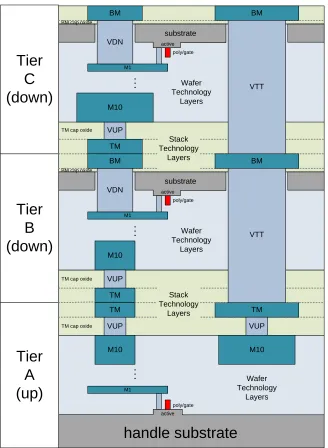
substrate M1 . . . active poly/gate M10 VUP TM
handle substrate
M1 . . . active poly/gate M10 VUP TM TM VUP M10 Stack Technology Layers Wafer Technology Layers Wafer Technology Layers Stack Technology Layers VUP TM substrate M1 . . . active poly/gate M10 Wafer Technology LayersTier
A
(up)
Tier
B
(down)
Tier
C
(down)
BM cap oxide
VDN BM
VTT BM
BM cap oxide
VDN BM
VTT BM
TM cap oxide
TM cap oxide TM cap oxide
Figure 3.2 Cross section of the first three tiers of the FreePDK3D45 technology.
The complete list of cross-sectional layers generated by the FreePDK3D45 technology is
more than 100, which is too much detail for a system-level thermal analysis. Hence this tool
substrate b) active and c) metal. This division is chosen because of the differing thermal
properties of each portion. First, substrates typically have much higher conductivity than
other portions and are therefore modeled separately. Second, the active layer is modeled
separately, because it is typically the place where the majority of heat is generated. Third, the
metallization layers can be collectively viewed as a metal-insulator composite and are
typically where most of the temperature rise occurs in a 3D stack. Thermal conductivity in
such composite materials can be difficult to predict, because the conductivities of materials
and insulators differs by 100 to 1000. Accurate prediction requires a detailed description of
the structure and a set of complex matrix solutions to find the thermal conductivity (k) to be
used with Fourier’s law of heat conduction in the form of a 3x3 matrix tensor.
In the absence of detailed layout information, Pathfinder3D constructs a basic unit cell
that depends on the metal densities for each layer (as a 0 to 1 range) and its routing direction
(horizontal, vertical or cut). Performing the exact matrix calculation of the conductivity
tensor for the basic unit cell is straight-forward and described in detail in Pathfinder3D
tutorial [17]. However, the exact conductivity tensor is currently not computed, because it is
time consuming to code and debug. In the meantime, Pathfinder3D calculates upper and
lower bounds on the diagonal elements of the conductivity tensor (kx, ky, and kz). The
off-diagonal elements tend to be small, since most of the wires tend to follow the x, y, and z axes.
Here we describe how these conductivity bounds are calculated. The two simplest
as a parallel combination of conductances. If a composite material consists of a series of
material segments that are orthogonal to the direction of heat conduction, then the material
can be viewed as a series combination of conductances. Most materials will not directly fall
into these two categories However, there are a large number of structures (including
rectangular meshes) for which we can apply a combination of the parallel and orthogonal
equivalent calculations. The order in which we apply them has different assumptions on how
heat flows and can therefore be viewed as bounds on the equivalent conductivity. The upper
bound can be calculated considering a unit cell consisting of N orthogonal segments, each
with Mj parallel cross-sections. In this case, a parallel equivalent can be assumed for each
segment, and an orthogonal equivalent can be assumed for the segments collectively. The
equivalent parallel-orthogonal conductivity can be calculated as follows:
_ _ 1 , 1 , 1 , i
eq par orth N i M
i i j
j i j
k L A k
(1) assuming, , 1 1 1, 1. i M Ni i i j
i j L A
(2)This model differs from the exact equivalent conductivity, because it assumes perfect
heat spreading between the segments. In reality, heat spreads gradually through the material
when a temperature gradient is applied. Therefore, keq-par-orth can be viewed as an
upper-bound on the conductivity of the composite material. The lower upper-bound of equivalent thermal
each with Mj orthogonal segments. In this case an orthogonal equivalent can be assumed for
each cross-section, and a parallel equivalent can be assumed for the cross sections
collectively. The equivalent orthogonal-parallel conductivity can be computed as follows:
_ _ 1 , 1 , , i N i eq orth par M
i i j
j i j A k L k
(3) assuming , 1 1 1, 1. i M Ni i i j
i j A L
(4)This model differs from the exact equivalent conductivity, because it assumes no heat
spreading between the cross-sections. Therefore, keq-orth-par can be viewed as a
lower-bound on the conductivity of the composite material. In Pathfinder3D, these approximations
are applied to the basic unit cell that is constructed for each technology. The upper-bound,
keq-par-orth is used for kx and ky values, while the lower-bound, keq-orth-par is used for
the kz value.
The tool also considers the effect of TSVs in equivalent thermal conductivity calculation.
TSVs are essentially cut-layers, but depending on the start and stop layers defined for each
TSV in the technology file, they are likely to coincide with a wafer-technology layer
(i.e. horizontal or vertical routing layer or another cut layer). In these cases, the density of the
the wafer-technology routing layer and the TSV. This is akin to an upper-bound on the
conductivity impact of a TSV.
Pathfinder3D also calculates the equivalent specific heat capacity of metal-insulator
composite using the similar approach used for equivalent thermal conductivity calculation.
This parameter is used in transient thermal simulation.
B. Rough Floorplan
In the pathfinding flow, a rough floorplan and power profiles of floorplan blocks are
required for the thermal simulations. Pathfinder3D allows users to specify textual description
of their floorplan. They can define the dimensions of basic building blocks of each tier in the
3D stack as macrocells. Each macrocell can have multiple sockets representing ports of the
block. Users can then replicate these macrocells as different instances at various locations in
their corresponding tiers by specifying the coordinates and the connections among instances.
The instances connection information can be imported from the system description defined in
the front end. After that, a simple routing tool is applied to estimate global wire length and
repeaters are added for those wires based on a minimum delay insertion algorithm. This
allows estimating interconnect power of the design. In this way a full floorplan can be
constructed. Currently users can specify the total power value for each instance in the
floorplan in a separate power stimulus file.
The tool reads the floorplan and creates an Open Access layout. In layout, each macrocell
is mapped with three layers namely; substrate, active and metal-insulator composite
file and assigns the total power of each instance to the active layer of that instance. Currently
power is uniformly assigned to complete area of macrocell. At this stage, the inputs to the
thermal simulator are ready.
C. Thermal simulation
The Pathfinder3D toolset consists of a physical thermal extractor, WireX [12]. WireX
reads the layout generated from rough floorplan and creates a linear resistive and capacitive
thermal netlist. It uses the thermal conductivity, specific heat capacity and other material
properties of the composite model to generate this netlist. WireX meshes the layout and
discretizes it in cuboids. Each cuboid is modeled using a thermal resistor from the center of
cuboid to each face with a thermal capacitor from center terminal to the thermal ground. The
user is able to control the fidelity of mesh. Usually for fast thermal simulation in pathfinding
phase the resolution of mesh is kept low. For steady state thermal analysis, the extractor
generates a thermal modified nodal admittance matrix (Y) and power vector (J). Then, Yv = J
is solved by a linear sparse matrix solver to get the temperature vector (v).
The WireX tool currently supports only one style of boundary condition, which is a
perfect heatsink on one face of the stack and adiabatic on all other faces. The perfect heatsink
is assumed to be connected to the first tier specified in the stack technology. All temperatures
will be reported as rise above the heatsink. For absolute temperatures, the temperature
accurate assumption. However, users have flexibility to model portions of the package and
heatsink as composite layers in the Pathfinder3D technology file.
The transient thermal simulation requires a transient solver. Currently Pathfinder3D does
not include any transient solver. However, it can generate a netlist compatible with HSPICE
or the open source circuit simulator fREEDA [13 from 3DIC]. fREEDA provides various
techniques [44] to speed-up the transient electro-thermal simulation which can be very useful
for pathfinding studies.
D Global routing and wire length estimation
Aside from thermal analysis, pathfinder3D also provides a global routing tool. The tool
reads the floorplan and blocks connection information, performs trial route under
area/capacity constraints. In the case of 3D integration, the TSVs are also taken into account.
An important benefit of 3DIC is the global wire reduction due to small chip area and vertical
logics. In that case, it is important to evaluation the benefit before implementing detailed
design.
3.3 Transaction-level Simulation with GEMS framework
3.3.1 Event-driven Simulation
In GEMS framework, different modules are managed by a scheduler via event queue.
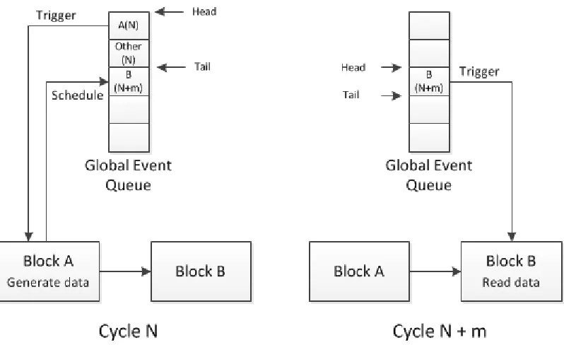
The event queue schedule mechanism is the kernel of this simulator. Figure 3.3 shows how
are two blocks A and B are connected with each other, and A would like to send data to B. To
simulate that behavior, first, we need to build the connection between A and B. In the design
partitioning phase, both blocks are instantiated and the consumer of A is pointed to B. During
the simulation, the scheduler will check the event queue every cycle, and in cycle N, block A
is scheduled and to be triggered. Then A is executed and generates data for B, meanwhile, A
will send a schedule request to the event queue to schedule its consumer B. Assume that it
takes m cycles for a to generate the data and send it to B due to link latency, A would
schedule B to trigger B m cycles later. The events in event queue are checked every cycle,
and in cycle N+m, B is executed. B reads the data generated by A m cycles before. In that
example, both A and B perform their function upon triggered. Since the schedule request and
trigger block cannot happen during the same cycle, the execution order of blocks in the same
cycle does not matter. In case a block is scheduled multiple times to execute at the same time,
all schedule requests are merged and the target block executes once in that cycle. The
event-drive simulator makes it easy to build complex system. Designers can add new blocks by
using this event queue mechanism while do not need to arrange the execution order for each
Figure 3.3 Block communication with event-driven simulator
3.3.2 Adding Interconnect Model
GEMS framework is built for multi-core and implements various cache protocols to
address the coherency problems. It also has some simple network to simulate the interconnect
behavior. However, the simple network provided within GEMS framework does not maintain
a detailed timing model and cannot capture the behavior for interconnect-centric system such
as Network-on-Chip (NoC). In this chapter, we present an approach to add interconnect to
GEMS for a circuit-switched NoC.
First, we need to identify the interface between interconnections and other blocks such as
cores and caches. In GEMS framework, cores, caches and interconnections are sub-systems
in which multiple copies such as cache banks, routers can be instantiated. Those sub-systems
create a new interconnection sub-system, we need 1) create the network sub-system
including routers and arbiters inside the network. 2) Create message buffers connecting
blocks outside the interconnect sub-system.
After setting the interface up, the next step is port bonding and consumer setting. As we
showed before, all blocks need to “schedule” their outputs to the event queue so that they can
be triggered correctly. In our case, interconnects can be divided into two parts: data-path and
control-path. Data packets in data-path are transferred from router to router or router to
core/cache. Each router should set its output block as consumer and schedule the consumer if
there is pending data ready to send out. Meanwhile, a shared queue is created for the 2
routers to store the data. In control-path, request and grant signals are transferred instead of
data. We have a centralized arbiter which controls all the traffic inside the interconnections.
All routers should set the arbiter as their consumer and schedule the arbiter if there is a
pending data to send. That will cause multiple schedule event occurs at the same time, but
since we can merge the event as mentioned above, the arbiter can be triggered correctly
without request loss. And since the arbiter decides which router(s) can send data, it also
needs to set all routers as its consumer and schedule the routers based on arbitration result.
Figure 3.4 Example to add interconnections to GEMS framework
3.4 Summary
In this chapter, a pathfinding flow for system-level design evaluation. The flow is divided
into two parts: front-end part and back-end part. The objective of front-end part is to generate
system description for simulator and back-end part. In this flow, we incorporate a TLM
simulator from GEMS framework. The TLM simulator can build various systems with

![Figure 2.4 Pathfinding flow presented in Rako’s work [25]](https://thumb-us.123doks.com/thumbv2/123dok_us/1743581.1223190/28.612.118.517.82.562/figure-pathfinding-flow-presented-rako-s-work.webp)
![Figure 2.5 Physical-analysis flow used in SpyGlass3D [26]](https://thumb-us.123doks.com/thumbv2/123dok_us/1743581.1223190/30.612.113.532.159.630/figure-physical-analysis-flow-used-spyglass-d.webp)
![Figure 2.6 TLM-2.0 Architecture [31]](https://thumb-us.123doks.com/thumbv2/123dok_us/1743581.1223190/33.612.114.519.294.597/figure-tlm-architecture.webp)