Implementation and Comparison of Split Path
Data Driven Dynamic Logic Topologies for
8-Bit Booth Multiplier Using 180nm
Technology
M.Ashwini
1, M.Kasetty Ram babu
2PG Student, Dept. of ECE, Nagarjuna College of Engineering and Technology, Devanahalli, Karnataka, India1
Assistant Professor, Dept. of ECE, Nagarjuna College of Engineering and Technology, Devanahalli, Karnataka, India2
ABSTRACT: In this paper, an efficient proposed design has been implemented in multiplexer that has designed by
using transmission gates. Transmission gate based design enhances the speed of the desired system. It uses the data transmission instead of computating the data depending on the input. In this work, three Logical structure of 8×8 radix-4 booth multipliers are implemented in 1.8V 0.18um CMOS technology, with as follows SPD3L, Modified SPD3L and MUX based. Depending on the input patterns, the modified SPD3L technique saves 10 to 30% power and is slightly faster than SPD3L and MUX based technique saves power 10 to 75% compared to modified SPD3L technique and its delay will be same as modified SPD3L. Simulations and designs are performed on Cadence Virtuoso and Spectre tools using UMC 0.18um technology.
KEYWORDS: Split path data driven logic (SPD3L), Booth multiplier, Transmission gate, dynamic domino logic.
I. INTRODUCTION
The main advantage of dynamic domino logic gates over CMOS static gates are they are faster and requires less area, but the overall power dissipation can be substantially higher than that of static gates [1]. About 10 to 35% of overall power is consumed due to the distribution of global clock network, thus preventing the use of domino circuit in low power design [2]. This drawback is removed in data driven dynamic logic (D3L) by completely omitting the clock network where the dynamic node is pre-charged by the subset of input signals rather than global clock [3]. Power consumption is significantly reduced but the pre-charge propagation path delay adversely affects the speed performances and limits the power delay product. In fact the cascaded pre-charging networks may cause a slower propagation path than the corresponding evaluation path thus dominating the critical path delay.
In cascaded design of D3L, the pre-charging takes place through all the pull up networks (PUNs) in series. Hence, the path becomes slower and in order to make pre-charging faster all the PMOS transistors in PUNs are made wider. This in turn increases the load capacitance of pre-charge inputs resulting in larger dynamic power consumption. This problem is avoided in a split-path data driven dynamic logic (SPD3L) by splitting the dynamic node into „n‟ number evaluation paths causing reduced load capacitance which in turn results in reduced power dissipation as well as delay [2]. Though SPD3L improves power consumption and delay compared to D3L counterparts, still it consumes considerable amount of power to reduce that power proposed a modified SPD3L in which the static CMOS gates are used with low fan-in inputs in conjunction with SPD3L, which decreases the power with enhanced speed due to reduced number of transistors used.
Transmission gate or it can also be called as analog switch is defined as an electric element that selectively pass or block a signal level from the input to the output depending on control signal and it does not depend on input signal and the delay can be reduced. The proposed design is implemented using multiplexers which are designed by TG logic technique. However multiplexers output always depends on the select line, depending on the select line multiplexers passes whatever input data present at the input node to the output node without computation operation and hence delay and power will be reduced.
II. RELATED WORK
A new family of low-power dynamic logic called Data-Driven Dynamic Logic (D3L) is introduced. In this logic family, the synchronization clock has been eliminated, and correct sequencing is maintained by appropriate use of data instances. Then, it is shown that replacement of the clock with input data implies less power dissipation without speed degradation compared to conventional dynamic logic [6].The new full adder circuits using combination of the recently proposed split-path data driven dynamic logic and data driven dynamic logic. Based on the logic function realized, the adders were characterized for performance and power consumption. The adders were then further deployed to evaluate the impact of sum and carry propagation delays on the performance, power of these systems .In this way, the number of series-connected pre charging transistors and the gate input capacitance are minimized with remarkable benefits in terms of dynamic energy dissipation and computation speed [7].
Data-pre-charged dynamic logic, also known as data-driven dynamic logic (D3L), is very efficient when low-power constraints are mandatory. Differently from conventional dynamic domino logic, which exploits a clock signal, D3L uses a subset of the input data signals for pre-charging the dynamic node, thus avoiding the clock distribution network. Power consumption is significantly reduced, but the pre-charge propagation path delay affects the speed performances and limits the energy–delay product (EDP) improvements [8].Dynamic logic style is used in high performance circuit design because of its fast speed and less transistors requirement as compared to CMOS logic style. But it is not widely accepted for all types of circuit implementations due to its less noise tolerance and charge sharing problems. Domino logic uses one static CMOS inverter at the output of dynamic node which is more noise immune and has less capacitance at the output node. In this paper we have proposed a novel circuit for domino logic which less noise at the output node and has very less power-delay product (PDP) as compared to previous reported articles [9].
Multipliers are the key components of many high performance systems such as FIR filters [10], microprocessors, digital signal processors, etc. A system‟s performance is generally determined by the performance of the multiplier because the multiplier is generally the slowest clement in the system [12].
II.SPD3L DESIGN
Fig. 1 Implementation of a function using SPD3L design where dynamic node is split in „n‟ separate sub-evaluation paths having single PMOS transistors each .
III. MODIFIED DESIGN
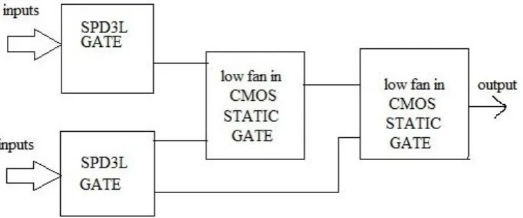
In this design the digital logic function is not implemented completely in SPD3L style but is combined with static CMOS gates. For low fan-in designs, the static CMOS gates have low loading capacitance which leads to low dynamic power consumption and high speed of operation. This is the key point in enhancing the efficiency of SPD3L. In realizing any digital block it is mandatory that the CMOS gate is placed after the SPD3L gate. Fig. 2 is an example which shows the implementation of modified SPD3L design.
Fig. 2 Implementation of a logic function in mixed style.
IV.TG LOGIC BASED DESIGN
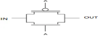
The schematic diagram (Fig 3) includes the arbitrary labels for IN and OUT, as the circuit will operate in an identical manner if those labels were reversed. This design provides true bidirectional connectivity without degradation of the input signal.
Fig .3 Schematic representation of a transmission gate.
V. MULTIPLIER DESIGN
Multiplication is the most common mathematical operation frequently performed in Digital Signal Processing applications. To enhance its efficiency several algorithms have been proposed. In this paper the multiplier is implemented with Booth‟s algorithm [1]. It is used to calculate the product of two n bit signed numbers. Booth multiplication involves two techniques to reduce the delay.
1) To reduce the number of partial products.
2) To increase the speed at which the partial products are added.
Fig. 4 shows the basic architecture of Booth multiplication. Radix-4 Booth multiplier comprises four logic blocks namely (a) BOOTH ENCODER is used for encoding multiplier bits and reduces the number of partial products, (b) PARTIAL PRODUCT GENERATOR is used to generate partial products, (c) CARRY LOOKAHEAD ADDER is used to add the partial products generated.
Fig. 4 Booth multiplier architecture.
VI.MULTIPLIER DESIGN IN SPD3L, MODIFIED SPD3L AND PROPOSED STYLE
In this paper 8×8 radix-4 booth multiplier is implemented. In this multiplier design booth encoder, partial product generator has been implemented in SPD3L, modified SPD3L and TG based mux design.
A.BOOTH ENCODER
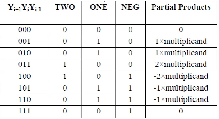
In this block it takes input from multiplier Y and encodes into the three outputs namely ZERO, ONE, and TWO shown in fig 5.The Booth encoder logic circuit can be easily constructed by using below table.
PARTIAL PRODUCT GENERATOR SIGN EXTENTION Radix-4 BOOTH ENCODER CARRY LOOKAHEAD ADDER (Compressors) 16 bit Final product
8bit multiplicand X
8bit
TABLE I
Encoding of radix-4 Booth multiplier
The above table I show the encoding of radix-4 Booth multiplier and also indicate what will be the output of booth encoder when we apply input from 000 to 111. By using the table we can also do the practical calculations for final product after obtaining the partial products from partial product generator.
Fig.5 figures show the implementation of booth encoder in three styles. For 8 bits 4 booth encoder block will be required.
a) SPD3L b) Modified SPD3L c) proposed design (mux based)
B.PARTIAL PRODUCT GENERATOR
Based on the output of Booth encoder block the PPG block will select either Xj or Xj-1 and produce complement
depending upon NEG value. Fig. 6 shows the logic diagram of PPG block. Multiplication by 2 is achieved by shifting the bit by one position towards left and negation by taking two‟s complement of it. Since there are four booth encoders there will be four PPG rows.
a) SPD3L b) modified SPD3L c) proposed design(mux based)
Fig. 6 PPG blocks in three designs.
Fig. 7 illustrates how we can design the architecture for booth multiplier to generate partial products using Booth encoder and partial product generator. The below fig 7 shows general architecture of booth encoder and partial product generator . By using fig 7 we can easily implement architecture to generate the partial products.
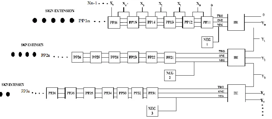
C.SIGN EXTENTION
Sign extention method is used in booth multiplier to easily add the partial products of each stage. The sign extention is performed by using output of the booth encoder.The booth enocder neg output of each stage or first partial product of each stage can be used for sign extention and addition operation of partial products that as shown in fig 8 below.
Fig. 8 shows sign extention for 8×8 booth multiplier
D. CARRY LOOKAHEAD ADDER USING COMPRESSORS
This blocks are used to add the partial products that were produced in PPG module,full adder,4:2 Compressor,7:4 compressors,9:6 compressors are used for addition of partial products.the compressors are designed by usign full adders 4:2 compressor is shown in fig 9 below. 7:4 compressor is designed by using 4:2 compressor by adding one more full adder stage and 9:6 compressor also designed by using 7:4 compressor and adding one more full adder stage.
Fig. 9 4:2 Compressor
VI.IMPLEMENTED DESIGNS AND SIMULATED RESULTS
Fig. 10 Implemented architecture of 8×8 booth encoder and partial product generator.
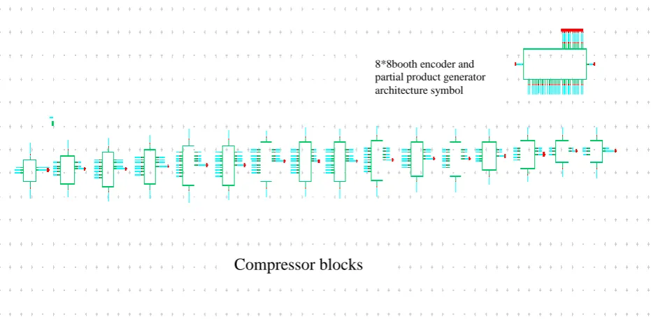
The fig 11 shows schematic design of the complete design of 8×8 booth multiplication. The above symbol is created by 8×8 booth encoder and partial product generator architecture and below blocks are compressor blocks that are used to add the partial products.
Fig. 11 complete design of 8×8 booth multiplication
8*8booth encoder and partial product generator architecture symbol
The fig.12 shows simulation results of the 8bit multiplication using radix-4 8×8 booth multiplier. In fig .12 X0 to X7 indicates the multiplicand inputs and Y0 to Y7 indicates multiplier inputs and S0 to S15 indicates final output product of the multiplier.
TABLE II
Power and Delay comparision
DESIGN Avg. Power Avg. Delay
SPD3L 21.85×10⁻³ 20×10-6
Modified SPD3L 2.809×10⁻³ 10×10-6
Proposed design(mux based) 1.20×10⁻⁶ 9.99×10⁻⁶
The above table II indicates the avarage power and delay of all designs. From the table SPD3L consumes more power than modified SPD3L and proposed design consumes less power than modified SPD3L design.
VII.CONCLUSION
Using three design styles 8×8 radix-4 Booth multiplier is implemented. The modified SPD3L design reduces the power 10 to 30% and slightly faster than SPD3L but the proposed design reduces the power 10 to 75% speed of operation will be slightly same as the modified SPD3L. The proposed design can be applied where speed and power is a constrain. The modified SPD3L design can be applied where low fan in gates are used. In implementing this design one can use large size static gates to boost the speed but it will deteriorate the power factor. The implementation of new multiplexer based design by using transmission gates to reduce the power factor and boost the speed but it will retain the area size and hence a trade-off exists.
REFERENCES
[1] J. M. Rabaey, A. Chandrakasan, and B. Nikolic, Digital Integrated Circuits. Englewood Cliffs. NJ: Prentice-Hall, 2003.
[2] F. Frustaci, M. Lanuzza, P. Zicari, S. Perri, and P. Corsonello, “Low power split path data driven dynamic logic,” IET Circuits, Devices Syst.,
vol. 3, no. 6, pp. 303-312, Dec. 2009.
[3] Rafati R., Fakhraie S.M., and Smith K.C., “A 16-bit barrel-shifter implemented in data-driven dynamic logic (D3L),” IEEE Trans. Circuits
Syst. I, 53, no. 10, pp. 2194-2202, 2006.
[4] Rafati R., Charaki A.Z., Chaji G.R., Fakhraie S.M., and Smith K.C., “Comparison of a 17 b multiplier in dual-rail domino and in dual-rail D3L (D4L) logic styles,” Proc. IEEE Int. Symp. Circuits and Systems,
May 2002, vol. 3, pp. 257–260.
[5] S.-R. Kuang, J.-P. Wang, and C.-Y. Guo, “Modified Booth multipliers with a regular partial product array,” IEEE Trans. Circuits Syst. II, Exp. Briefs, vol. 56, no. 5, pp. 404–408, May 2009
[6] R. Rufati', S. M. Fukhraie', K. C. Smith2 “Low-Power Data-Driven Dynamic Logic (D3L)”, ISCAS 2000 - IEEE international Symposium on Circuits and Systems, May 28-31, 2000, Geneva, Switzerland
[7]. Fathima Nazrin.K Dhivya.V M.Darani Kumar “Hybrid Low Power Design for Adders Using SP-D3L”, International Journal of Advanced Information Science and Technology (IJAIST) ISSN: 2319:2682 Vol.12, No.12, April 2013
[8]. F. Frustaci M. Lanuzza P. Zicari S. Perri P. Corsonello “ Low-power split-path data-driven dynamic logic”, IET Circuits Devices Syst., 2009, Vol. 3, Iss. 6, pp. 303–312
[9]. PREETISUDHA MEHER, K. K. MAHAPATRANational Institute of Technology, Rourkela “High-Speed and Low-Power Dynamic Logic Style” International Journal of VLSI and Embedded Systems-IJVESVol 04, Issue 03; May - June 2013.
[10]A. D. Booth, “A Signed Binary Multiplication Technique,” Quarterly J. Mechanical Applications in Math., vol. 4, part 2, pp.236-240,1951. [11]John G.Proakis, Dimitris G. Monolakis, “Digital Signal Processing,Principles,Algorithms, and Applications”, Fourth Edition.
[12] A. Dandapat, S. Ghosal, P. Sarkar, D. Mukhopadhyay (2009), “A 1.2-ns16×16-Bit Binary Multiplier Using. High Speed Compressors”, International Journal of Electrical, Computer, and Systems Engineering, 2009, 234-239.
[13] J. Gu, C.H.Chang (2003), “Ultra low voltage low power 4-2 compressor for high speed multiplications”. Circuits and Systems,2003.ISCAS ‟03. Proceedings of the International Symposium, vol. 5, May 2003, 321-324.