IJEDR1801135
International Journal of Engineering Development and Research (
www.ijedr.org
)
784
Design of Modified Booth Encoder based Low Power
Multiplier
1
Suresh H,
2Beena A O
1Graduate Associate, 2Assistant professor, Dept of ECE, Saintgits College Of Engineering, Kottayam
Abstract—Multipliers are one of the major power consuming elements in digital signal processing applications. Multiplications occur in digital signal processing applications like FIR filters, FFT, DCT, convolution etc. The use of a low power multiplier will provide a significant reduction in power for the digital signal processing applications. This paper discuss about the design of a low power multiplier based on Booth encoding technique and Spurious Power Suppression Technique (SPST). A normal multiplier performs the multiplication operation by repeated shifting and addition process. For an n-bit multiplier there will be n additions of n-bit numbers. In this design the Booth encoding technique reduces the number of additions by half and the SPST reduces the unwanted transitions in the adder.
Keywords—booth encoder, spurious power supperssion technique, low power.
________________________________________________________________________________________________________
I. INTRODUCTION
The design of low power and high performance modules are given great importance nowadays. The use of a low power module help in reducing the heat generated in the final product and thereby help in improving the life of the product. Multipliers are the frequently used module in digital signal processing and other common applications. Usually the multiplication process can be considered as a sequence of addition and shift operations. After each addition operation a partial product is generated. The operation a multiplier can be decomposed into two operations, the generation of partial products and accumulation of the partial products. The performance of the multiplier can be increased by reducing the number of partial products being generated during the multiplication process. This also helps in reducing the power consumed by the multiplier. A good multiplier should have a compact physical design, high speed of operation and low power consumption. To reduce the power consumed by a VLSI design it is better to reduce its dynamic which is a major part of total power dissipation. The switching activity of the design will decide the dynamic power. In this paper will be discussing about methods to reduce the switching activity of the multiplier by employing Booth encoding technique and SPST.
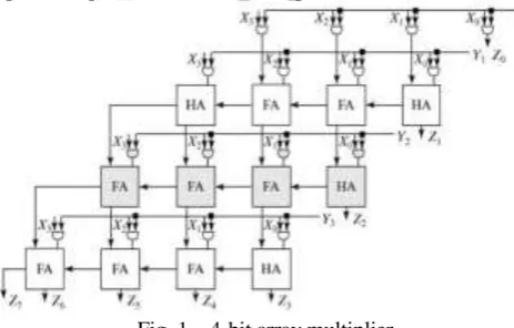
forms the product bit all at once thus making it a fast way of multiplying two numbers. Only delay is the time for the signals to propagate through the gates that forms the multiplication array [5]. Array multipliers were very popular due to the regularity in its physical design [6]. A normal array multiplier accepts two inputs, the multiplier and the multiplicand. The partial products are generated by AND operation of the multiplicand with each bit of the multiplier. Each successive partial products are shifted one bit to left and are added together to obtain the product. An array multiplier is the most basic form a multiplier. It is now rarely being used for digital signal processing or other applications. Some of the drawbacks of an array multiplier are its delay in operation, power and area consumption.
Fig. 1. 4-bit array multiplier
IJEDR1801135
International Journal of Engineering Development and Research (
www.ijedr.org
)
785
consumption can be reduced. The next section discusses about the design a multiplier in which the unnecessary computations avoided.II. OPERATION OF NORMAL ARRAY MULTIPLIER
Array multiplier is an efficient layout of a combinational multiplier. Multiplication of two binary numbers is done and the product is obtained by using a combinational circuit that
III.BOOTH ENCODER BASED MULTIPLIER
Fig. 2. Addition operations with spurious transitions.
The booth encoder based multiplier uses the booth encoding algorithm to reduce the number of partial products produced during a multiplication operation. It also employs a spurious power suppression technique to modify the adder modules to reduce the power dissipated in the adder.
The booth encoder based multiplier uses the following modules for its operation: A. SPST Detection Logic
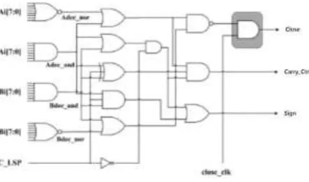
SPST has been discussed in [3] [4]. In this paper the SPST is used to construct an efficient adder circuit for the addition of partial products. The SPST detects the spurious transitions in additions and prohibit them from occurring and thereby reduce the power consumed. Some examples of spurious transitions are shown in Fig. 2. Case 1 shows the addition of
B. SPST Adder
Fig. 3. SPST detection Logic
two positive numbers without and with carry transition from Least Significant Part (LSP) to Most Significant Part (MSP). Case 2 shows the addition of one positive number and one negative without and with carry transition from LSP to MSP. Case 3 shows the addition of two negative numbers without and with carry transition from LSP to MSP. In these cases the calculation of MSP is unnecessary and can be avoided. The SPST detector is shown in Fig. 3, it takes the MSP of the multiplier & multiplicand and the carry from LSP addition(C_LSP) as inputs and produces the following signals:
‒ Close: This signal is used to detect whether the MSP of can be directly found or not. ‒ Carry_Ctrl: This signal represent the least bit of the MSP of sum output.
IJEDR1801135
International Journal of Engineering Development and Research (
www.ijedr.org
)
786
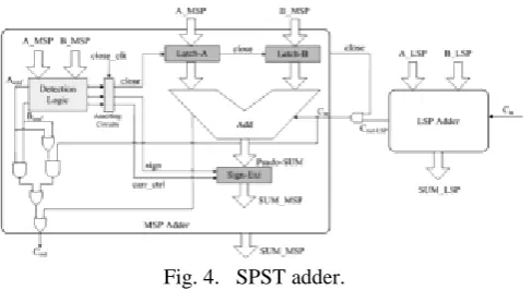
Carry_Ctrl and Sign outputs of the SPST detector. If the Close output of the SPST detector is high, then the normal addition of the MSP is performed. The block diagram of SPST adder is shown in Fig. 4.Fig. 4. SPST adder.
The Latch-A and Latch-B are realized using AND gates. The design of Latch is shown in Fig. 5. The Sign-Ext module is designed using OR gates. The internal structure of Sign-Ext is shown in Fig. 6.
Fig. 5. Latch using AND gates
Fig. 6. Sign-Ext designed using OR gates
The Latch-A and Latch-B will be closed when the Close signal is Low and the output will be decided by the Sign-Ext module. If the Close signal is high the Latch-A and Latch-B will be transparent and the A_MSP and B_MSP signals will be passed to the adder and output will be the output of the adder.
C. Booth Encoder
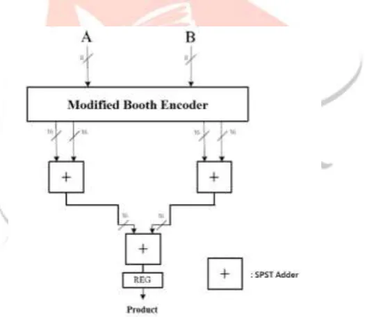
Booth encoding has been discussed in [1] [2]. The booth encoder generates the partial products based on the inputs. It generates the partial products based on the booth algorithm. Compared to the array multiplier the number of partial products generated in the booth encoder based multiplier will be half. The partial products are generated based on the bits in the multiplier input. The booth encoder groups the multiplier bits into groups of three and generates a partial product for each group. The multiplier bit grouping according to the booth encoding algorithm is shown in Fig. 7.
Fig. 7. Bit grouping of multiplier input
A zero is added at the right hand side of the multiplier input, and then the multiplier bits are made into an overlapping group of 3 bits. Then according to the bits in each group a value is selected from {-2, -1, 0, 1, 2}. These values are decided based on booth multiplication algorithm. The corresponding values for all the 3-bit combinations are shown in TABLE I.
IJEDR1801135
International Journal of Engineering Development and Research (
www.ijedr.org
)
787
The corresponding values are multiplied with the multiplicand to generate the partial product. In this radix-4 booth encoding is applied. There will be five possible values to be multiplied with the multiplicand to generate the partial products. These multiplications can be performed by simple shifting and compliment operations. The multiplication by 2 can be done by one bit left shift, -2 by one bit left shift and compliment. The multiplication by -1 is just a compliment operation. For an 8x8 multiplier there will be 4 partial products. After the multiplication with booth encoder value, to make the partial products 16-bits some shift operations are done. For the first partial product 8 bit arithmetic right shift is done. For the second partial product 6 bit arithmetic right shift is done and then 2 bit left shift. For the third partial product 4 bit arithmetic right shift is done and then a 4 bit left shift. For the forth partial product 2 bit arithmetic right shift is done and then a 6 bit left shift. After these shifting operations the four partial products will become 16-bit each. Then these partial products are added together using 2 levels of SPST adders. The block diagram of the booth encoder based adder is shown in Fig. 8. The modified booth encoder module takes two 8-bit inputs, the multiplier and the multiplicand. It generates four partial product outputs of 16-bit each. These four partial products are added together to generate the product output.Fig. 8. Booth encoder based 8x8 multipier. IV. RESULTS
IJEDR1801135
International Journal of Engineering Development and Research (
www.ijedr.org
)
788
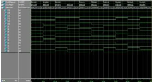
Fig. 9. Simulation result for Booth Encoder Based Multiplier.V. CONCLUSION
This paper discuss about the design of a low up to 30% based on simulation results. Moreover, the Booth encoder based multiplier will have better speed compared array multipliers. power multiplier which uses Booth encoding technique and SPST. The SPST adder will avoid the spurious addition operations by checking the inputs and blocking the unwanted additions thus it reduces the switching power dissipation. The Booth encoding technique will reduce the number of partial products by half. This will reduce the power dissipation and will also improve the performance. The booth encoder based multiplier is giving a power saving.
V.References
[1] Wen-Chang Yeh and Chein-Wei Jen, “High-Speed Booth Encoded Parallel Multiplier Design,” IEEE TRANSACTIONS ON COMPUTERS, VOL. 49, NO. 7, JULY 2000.
[2]Tushar V.More' Dr.R.V.Kshirsagar' "Design of Low Power Column Bypass Multiplier using FPGA" IEEE journal of solid-state' circuits' vol 31'pp 1535-1546'July 2011.
[3] ] [Rao P.V and Cyril Prasanna Raj and S. Ravi' "VLSI Design and Analysis of Multipliers for Low Power"' Fifth International Conference on Intelligent Information Hiding and Multimedia Signal Processing' 2009.
[4]Padmanabhan Balasubramanian and Nikos E. Mastorakis' "High Speed Gate Level Synchronous Full Adder Designs'" WSEAS TRANSACTIONS on CIRCUITS and SYSTEMS Issue 2' Volume 8' pp 290-300' February 2009.
[ 5 ] S an jiv K u m ar Ma n g al, R a h u l M .B ad gh ar e ,” FP G A Implemen tation of Low P ower P arallel Multiplier”,1 0th International Conference on VLSI Design,2007
[6] Hu ssain R,Shakkaf A.Y.M, “An efficient modified booth multiplier architecture”ICED 2008
[7] Rao P.V and Cyril Prasanna Raj and S. Ravi, “VLSI Design and Analysis of Multipliers for Low Power”, Fifth International Conference on Intelligent Information Hiding and Multimedia Signal Processing, 2009.
[8] Das.D, Rahaman.H “A Novel Signed Array Multiplier”Advances In Computer Engineering 2010 Conference
[9]. Shiann-Rong Kuang and Jiun-Ping Wang “Design of power efficient configurable booth multiplier” IEEE Trans. Circuits Syst. I Regular Papers vol. 57, no.3, pp. 568-580, March
2010.
[10]Vazquez.A,Antelo.E “Improved Design Of High Performance P ar alle l D ec im al M u lt ip lier s” IE E E T ra n s a ct io n s O n Computers,May 2010