Avoiding Hardware Vulnerability in IC Design
with Design-For-Trust Techniques
Sneha Nandini Bolloju, Ameet Chavan
Abstract: Un-trusted Computing Hardware platform is vulnerable to physical attacks such as probing of the memory bus or executing cold reboots. The proposed work implements Smart Memory with encryption and decryption control unit for not only securing data but also address. Through this control mechanism the data packets would appear indistinguishable to any adversary snooping into the memory bus. Smart memory further guarantees that the adversary cannot identify the type of memory access and prevent rollback of the memory state with unidentified packets. We demonstrate that Smart memory design isoptimized in power, performance and Area to other contemporary solutions. The overall smart memory system helps in developing a secure processor to store and process information at the edge level of a physical node as in the case of an IOT application.
Index Terms: Trusted computing, AES, RAM, Smart Memory, IOT, InvisiMem, Edge Level Computing. ————————————————————
1.INTRODUCTION:
Customized Service and Real-time processing are the two essential verticals for an embedded edge computing hardware platform.The need for privacy and secrecy has increased to meet the demands of growing population. With widespread data collection to generation day to day need from transmitting data through a secured channel to transmit and receive data till the storage medium everything could be altered to grab the potential data. These threats are needed to be addressed at the earliest as this data might be used to defame or harm a personal or a firm or even cause threat to a country in critical cases. To avoid data access to unauthorized personal and damage to the integrity of the data, data can be encrypted before storing or transmitting and decrypted to read the data using a significant cryptographic algorithm. An efficient algorithm suitable for this case is AES algorithm (Advanced Encryption standards). It provides a secured medium for the maintenance of data integrity. Also, AES is a most popular technique which is used for encryption and a widely accepted technology. The AES algorithm functions in four stages each of length 128 bits , such as; a sub Bytes (for implanting substitution bits), shift rows (used for cyclically shifting the bits to generate the state of the given matrix), mix columns (used to combine the linearly transformed nibbles in each column to perform mixing operations) and add round key (bytes of a state are a combination of each round key, with the help of the round key schedule each round key is derived from the cipher key).
2.System and IC Architecture:
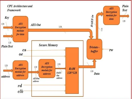
The IC Architecture of the Smart Memory consists of a traditional RAM along with the AES encrypter, decrypter modules, a key generator, a Tristate buffer and a clock frequency generator. The smart memory is a synchronous system, performing read write operations for a 128-bit data and 128 bit address. Hence, the key used is also of 128-bit data. The Smart Memory System consists of traditional memory along with encryption and decryption module (as shown in the below block diagram). Whenever a plain text is written in the memory it is encrypted with the help of an AES encrypter and a key such that the data is unique and remains undistinguishable by an intruder.
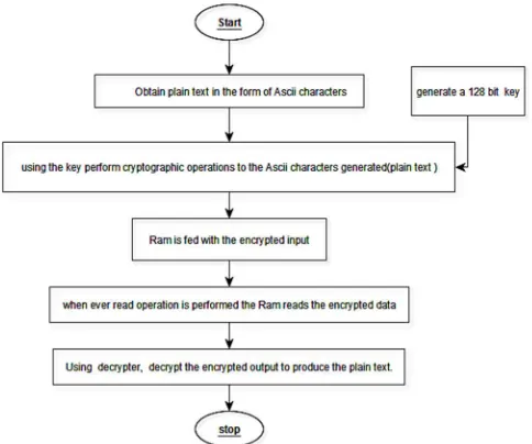
Figure 1: Flowchart for encryption and decryption process, describing the flow of data
————————————————
Sneha Nandini Bolloju is currently pursuing masters degree program in electronics and communication engineering in Sreenidhi Institute of Science and Technology, India. E-mail: [email protected]
3842 Figure 2: Block Diagram of Smart Memory with Encryption and
Decryption Control Module
And then it is written into the memory. Similarly, when an authorized user tries to read a data from certain location, he has to add the assigned key to the AES decrypter in order to decrypt the encrypted message before it is been read which will give the plain text that is been written into the RAM.
2.1 The Approach: AES is one of the widely accepted encryption models among various researchers and students due to its performance levels in different platforms with huge data. The reason for its efficient performance is the AES architecture. The parallel processing in the architecture helps in effective utilization of the resources and it occupies very small amounts of memory for implementation, this structure helps in instruction parallelism. It is widely accepted in various structures due to the various sizes of blocks it supports that are multiples of 32-bits. Also the fact that no linear or differential cryptographic analysis attacks are been proven on AES makes it more effective choice of encryption module in any architecture.
3. BACKGROUND WORK:
[1] Focuses on the vulnerabilities in VLSI design fabrication flow and elaborated on four DFTR techniques that have been developed by reusing VLSI test principles. They also have provided a survey on different DFTR techniques which aim to regain trust in designing an IC. [2] Discusses about Smart Memory, storage encryption, channel encryption and Fine-grained security. According to them when memory is associated with logic to which security functions are enabled such that it makes the program code only executable but not readable. i.e. It is made such that any adversary cannot read or alter the data. The storage encryption is used to secure the backup as well as archived data both at transit and storage levels. According to them in comparison with expensive storage encrypters, channel encrypter provides improved performances and economy for various applications and under different conditions.[3] proposed a testbed architecture with building blocks that are based on Radiation hardened Cells were implementto enhance the robustness of the design and elevate the trust factor (operationality) in harsh environments such as Space. [4] the authors have implemented FSM, LUT
For the purpose of detecting Trojans, the author has generated signatures for IC’s and obtained critical and noncritical path delays by using clock sweeping technique. According to them in the presence of process variations, identification of Trojan can be done effectively using statistical analysis methods. [17] The author says, high resolution can be obtained by deploying an embedded test structure known as time to digital converter. The adversary effects on hardware detection sensitivity with in die process variations can be reduced significantly by using chip averaging technique. It can also be used to measure the leakage currents. [18] Authors implemented a method to identify potential sets which are supporting multiple input trigger conditions these are accountable for available space silicon area, sufficient slack time and controllability in a design. [19] the authors have developed novel countermeasures, which allows trusted computing even when there is a Trojan present in the hardware. These developments focuses on new RTL-architecture features, reconfigurable logics, fragmentation schemes, various inputs applied and outputs obtained etc. [20] The author have designed different IPs basing on the global currents present in the QDI (Quasi Delay Insensitive) asynchronous circuits to evaluate behavior, sensitivity, capability of detecting of both in-line and off-line transient faults along with the detection techniques. Using this approach they have achieved automatic control on biasing the body in-order to balance both power and performance.
4. PROPOSED ARCHITECTURE:
A Traditional memory is not secured and the medium or the memory bus is more vulnerable to attacks which are a threat to the data. Data integrity can be maintained by avoiding these attacks by taking some precautions such as deploying encryption techniques before to preserve the data. Traditional methods of encrypting such as AES helps in preventing data breach. The proposed technique implements encryption of memory bus along with data and address to protect the data bus and address bus of the Smart Memory from these attacks. I.e. Memory bus is encrypted before channelizing data into the memory after the data is encrypted. Considering the worst-case scenario even if the memory bus is decoded, the adversary cannot breach into the data stored in the memory as it is also protected with encryption. The security for this system can be increased further by frequently changing the keys and maintaining different keys for encrypting data, data bus and address bus. These keys are generated remotely using a key generator. The communication or data transmission and reception can happen only when both the receiver and transmitter know the key. The table below explains the power analysis of the system architecture during its test. A traditional Ram alone functions at 4.20 W. But the smart memory works efficiently at a power of 14.97W (approximately). Though the power is high for smart memory it is robust and is proven to work effectively for 128-bit random key and plain text message.
Table 1: Power Analysis of the Proposed System Architecture
Type of operation Power
Address Encryption 2.45 W Address Decryption 2.35 W Data Encryption 2.45 W
Data Decryption 2.35 W
RAM 4.20 W
Smart Memory 14.97 W
5.SIMULATION RESULTS:
The simulation results (shown in figure 3) are obtained using Cadence Virtuoso simulator. The waveforms in the below figure shows the input and output to RAM as an encrypted text. To write the plain text of 128bit length into the memory it should be first encrypted using random key of the same length. The result is a Cipher text which is then stored into the traditional RAM. To read the stored data, we have to give the address location of the data we want to read along with the random key which was used in encryption to the decrypter. The decrypter then decodes the cipher text into the plain text and displays it. The encrypter and decrypter modules functions are sub-divided into 4 steps: 1. SubBytes, 2. ShiftRows, 3. MixColumns and 4. AddRoundKey. Combination of all these steps results in an encrypted plain text. For generation of a cipher text it needs 10 rounds of operations to be performed using each module. SubBytes: It is popularly called as S-Box. In this step the module involves replacement of all the variables present in the plain text using the lookup table provided. A 16*16 lookup table is used to substitute 8 bit data ShiftRows: This module is used to cyclically byte shifts the values in each row by a certain number of times with respect to its offset value. These operations are observed to avoid four individual encryptions within the plain text and independent block ciphers. In other words the number of bytes shifted in each row depends on the row number. MixColumns: This module performs invertible linear transformations to combine four bytes of in every column. In other words, it does mixing operations using multiplications along with XOR operations on the columns to combine the four bytes present in every column. AddRoundKey: In this module, from the encrypted key each round keys are derived using key schedules and each round key is combined with the bytes present in each state using XOR operations.
3844
The below shown physical design of the Smart memory is obtained from the Cadence simulator using SOC Encounter technology. This method helps to develop a prototype of the design to assess the floor-planning, for its timing, power and performance metrics. The steps involved in the construction of a physical design flow are Design Netlist, floor-planning, partitioning, placement, clock-tree-synthesis, routing, physical verification and GDSII generation. We have used the 180nm technology standard libraries to manufacture the physical design.
6. CONCLUSION
A smart memory functions just like any traditional RAM but with an added advantage of privacy and security. As it is built such that each data packet and address packet is made unique of its kind and remains undistinguishable by any intruder making it a resilient storage device. The technology involved in evolving the security parameters in the smart memory is a standard AES technique to encrypt and decrypt both the data and the address to provide simplified a solution using the popular AES for data encryption and integrity by optimizing Power and Performance.
Figure 4 - Output Waveforms: Smart Memory Simulations
REFERENCES
[1] Regaining Trust in VLSI Design: Design-for-Trust Techniques ByJeyavijayan Rajendran, student member IEEE, OzgurSinanoglu, Member IEEE and Ramesh Karri, Senior Member IEEE. Vol.102, No. 8, August 2014
[2] United States Patent Glew et al. Patent no. US 8,930,714 B2 by Andrew F. Glew, Hillsboro, OR (US); Daniel A. Gerrity, Seattle, WA (US) and Casey t. Tegreene, Bellevue, WA (US). Jan 6, 2015.
[3] Analysis of Radhard Standard Cells using a Digital Processing Element Architecture as Testbed. By SiluveruBakthaThukaram, Sneha Nandini Bolloju, AmeetChavan, International Journal of Recent Technology and Engineering (IJRTE) ISSN: 2277-3878, Volume-8, Issue-1, May 2019
[4] Low Power State Machine Design For AES
Encryption Coprocessor BY Liling Dong, Ning Wu and Xiaoqiang Zhang Vol II, IMECS 2015, March 18 -20 2015, Hong Kong.
[5] InvisiMem: Smart Memory for Trusted Computing ByShaizeen Aga and Satish Narayanasamy University of Michigan, Ann Arbor. International Symposium on Computer Architecture 2017 [6] Operating System Controlled Processor - Memory
Bus Encryption By Xi Chen, Robert P. Dick and Alok Choudhary Northwest University, 2008 Design, Automation and Test in Europe.
[7] Secure Processors Part I: Background, Taxonomy for secure Enclaves and Intel SGX Architecture. By Victor Costan, Ilia Lebedev and Srinivas Devadas. Computer Science and Artificial Intelligence Laboratory. Massachusetts Institute of Technology [8] Secure Processors Part II: Intel SGX Security
Analysis and MIT Sanctum Architecture By Victor Costan, Ilia Lebedev and Srinivas Devadas. Computer Science and Artificial Intelligence Laboratory. Massachusetts Institute of Technology [9] Circuit Design for Testing Standard Cell Libraries
By Renato P. Ribas, Vinicius Callegaro, Marcelo Lubaszewski, Andre Ivanov, Andre I. Reis UFMG Laboratory For Treating Information, 2012
[10] C – Element Model For Set Fault Emulation. By M. Arevalo - Garbayo, M. Portela – Garcia, M. Garcia- Valderas, C. Lopez-Ongil, L. Entrena. 978-1-4673-57057-0/13/$3.00 IEEE 2013
[11] Counterfeit Integrated Circuits: A Rising Threat In The Global Semiconductor Supply Chain By Ujjwal Guin, student member IEEE, Ke Huang, Member IEEE, Daniel DiMase, Jhon M. Carulli, Jr., Senior Member IEEE, Mohammad Tehranipoor, Senior Member IEEE and Yiorgos Makris, Senior Member IEEE. Vol 102, No 8, August 2014.
[12] Trustworthy Hardware: Identifying And Classifying Hardware Trojans By Ramesh Karri and Jeyavijayan Rajendran, Polytechnic Institute of New York University Kurt Rosenfled, Google, Mohammad Tehranipoor, University of Connecticut 0018-9162/10/$26.00 2010 IEE
[13] DARPA “Trust in IC’s” Effort By Dr. Dean Collins, Deputy Director, MTO 7 march 2007
[14] Assessing And Detecting Malicious Hardware In Integrated Circuits By Trey Reece in December 2014, Nashville, TN
[15] Hardware Trojan identification and detection Samer Moein, Fayez Gebali, T. Aaron Gulliver and Abdulrahman AlkandariInternational Journal on Cryptography and Information Security (IJCIS), Vol. 7, No.2, June 2017.
[16] A Clock Sweeping Technique For Detecting Hardware Trojans Imapacting Circuits Delay By Kan Xiao, Xuehui Zhang and Mohammad Tehranipoor 2168-2356/13/$31.00 2013 IEEE. [17] Detecting Delay Anomalies Introduced By
Hardware Trojans Using Chip Averaging And An On Chip High Resolution Embedded Test Structure By D. Ismari, C. Lamech, Swarup Bhunia, F. saqib and J. plusquellic
Rouzeyre Research Gate conference paper May 2013.
[19] Hardware Trojans – Prevention, Detection, CountermeasuresBy Mark Beaumont, Bradley Hopkins and Tristan Newby Defence Science and Technology Organization DSTO-TN-1012