Available online:
https://edupediapublications.org/journals/index.php/IJR/
P a g e | 1801An Efficient Implementation of Matrix Multipliers for
signal Processing on FPGA
A . Hari Priy a1
1Assistant Professor, Dept. of ECE, Indur Institute of Engineering. And Technology, Siddipet, Medak (D) India.
ABSTRACT : Matrix multiplication and Fast Fourier transform are two computational intensive DSP functions widely used as kernel operations in the applications such as graphics, imaging and wireless communication. Matrix multiplication is the kernel operation used in many image and signal processing applications. In this paper, we present the design and Field Programmable Gate Array (FPGA) implementation of matrix multiplier architectures for use in image and signal processing applications. The designs are optimized for speed which is the main requirement in these applications. First design involves computation of dense matrix vector multiplication which is used in image processing application. The design has been implemented on Virtex-4 FPGA and the performance is evaluated by computing the execution time on FPGA. Implementation results demonstrate that it can provide a throughput of 16970 frames per second which is quite adequate for most image processing applications. The second design involves multiplication of tri-matrix (three matrices) which is used in signal processing application. The proposed design for the multiplication of three matrices has been implemented on Spartan-3 and Virtex-II Pro platform FPGAs respectively.
KEYWORDS: FPGA, Matrix Multiplier, Systolic Array, FFT algorithms
I. INTRODUCTION
Matrix multiplication and Fast Fourier Transform are important tools used in the Digital Signal Processing applications. Each of them is compute-intensive portion of broadband beam forming applications such as those generally used in software defined radio and sensor networks. These are frequently used kernel operations in signal and image processing systems including mobile systems. Recently, in signal processing there has been a lot of development to increase its performance both at the algorithmic level and the hardware implementation level. Researchers have been developing efficient algorithms to increase the speed and to keep the memory size low.
On the other hand, developers of the VLSI systems are including features in design that improves the system performance for applications requiring matrix multiplication and Fast Fourier Transform. Research in this field is not only because of the popularity, but also because of the reason that, for decades the chip size has
decreased drastically. This has allowed portable systems to integrate more functions and become more powerful. These advances have also, unfortunately, led to increase in power consumption. This has resulted in a situation, where numbers of potential applications are limited by the power- not the performance. Therefore, power consumption has resulted to be the most significant design requirement in portable systems and this has led to many low power design techniques and algorithms.
II. LITERA TURE SURVEY
H.T.Kung and PhilipL.Lehman [5] reported matrix multiplication on systolic array. But FPGA implementation is not covered in their work. Again they have explained the operation on 2D systolic array. The 2D systolic array requires more number of processing elements interconnects and also as a result consumes more area. Also there is difficulty of VLSI implementation of it due to large numbers of interconnects.
Also latency is Order of n2. Kumar and Tsai [8] achieved the theoretical lower bound for latency for matrix multiplication with a linear systolic design. They provide trade-offs between the number of registers and the latency. Their work focused on reducing the leading coefficient for the time complexity. The latency becomes Order of n. Due to linear systolic design the number of interconnects gets reduced and also reduces the area by reducing the number of processing elements.
Mencer [4] implemented matrix multiplication on the Xilinx XC4000E FPGA device. Their design employs bit-serial MACs using Booth encoding. They focused on trade-offs between area and maximum running frequency with parameterized circuit generators.
Available online:
https://edupediapublications.org/journals/index.php/IJR/
P a g e | 1802number of CLBs divided by the maximum running frequency was used as a performance metric.
Ju-Wook Jang, Seonil B. Choi, and Viktor K. Prasanna [1] has developed a design to do the optimization of energy and area at algorithmic and architectural level. They have used a technique called domain specific modelling technique for the optimization at high level. Their algorithms and architectures use pipelining and parallel processing on linear systolic array. So the area and interconnects gets reduced But they considered the input word width directly. So if the size of input word increases the size of multipliers used in the design increases so by increasing the area and power consumption. Also it becomes difficult for VLSI implementation.
This problem of increase of word width was being solved by Sangjin Hong, KyoungSu Park [3] and by designing a very flexible architecture for a 2×2 matrix multiplier on FPGA. It has also mechanism to support 2’complement data. But they have not given any attempt to increase the throughput by pipelining or parallel processing. Again they didn’t propose block matrix multiplication. They have also not used the optimization procedure by constructing high level energy model. So in this article the proposed architecture uses algorithm for matrix multiplication on a linear systolic array to reduce the interconnects, uses pipelining and parallel processing to increase throughput there by reducing the latency. It also solves the problem of increasing size of the multipliers by using word width decomposition technique by modifying the algorithm and architecture. Then a high level model is constructed for the optimization of various parameters at high level.
In this section, we present the design and discuss the results of implementing matrix-vector multiplication which is computationally very intensive. It requires several multiply and add units. In DSPs, the overall performance is limited by the number of multiplications and additions that could be done in parallel. DSPs take several clock cycles to perform all the necessary multiply add operations. However, modern FPGAs on the other hand has large number of hardware resources embedded in the FPGA fabric itself such as DSP48 blocks, multipliers, Block RAMs, etc. It can provide higher and more efficient processing rates required by such applications if the algorithm is coded in a way to utilize these embedded resources efficiently. The objective of this paper is to realize a large matrix-vector multiplier for
image processing applications [51]. To achieve this, FPGA is used for faster and efficient realization.
III. M ATRIX-VECTOR MULTIPLICA TION: DESIGN A ND IM PLEM ENTA TION
A. M ath ematical Fo rmu latio n
We represent the vector C as (C1, C2...Cm)T and vector G
which represents the image data. According to the application, we want to multiply matrix S with vector C represented by the following equation
C=SG (1)
where, S is a Jacobian matrix. In the discrete form, it is required to find the unknown vector G from the known vector C, while S is treated as a constant matrix for simplicity. We can represent G by the following relationship
G=STC (2)
Where, ST is the transpose of S. Replacing ST by A,
mathematically; the above equation is approximated by the following relationship
G=AC (3)
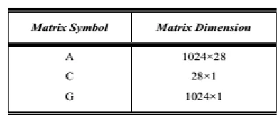
The key idea here is to calculate G using (3). The dimension of the given matrices depends on the application, which, in this case is summarized in Table 1.
Table 1: Matrix Dimensions
B. Hard ware A rch itectu re
This section presents the technique to design hardware architecture for implementing matrix-vector multiplication algorithm on FPGA. As can be seen from (3), matrix vector multiplication is the kernel operation. For efficient implementation and maximum speed-up, integer arithmetic is used. Since the floating-point arithmetic unit consumes more silicon real estate of FPGA and are slower as compared to integer arithmetic, we used integer arithmetic for our designs.
Available online:
https://edupediapublications.org/journals/index.php/IJR/
P a g e | 1803adopted for the matrix-vector multiplication. The matrix– vector multiplication is performed by broadcasting rows of matrix A and multiplying the corresponding column elements of vector C. Following operations are involved:
• Reading individual row elements of matrix A and individual column elements of vector C
• Storing them in internal buffers row and column wise respectively
• Multiplying row and column elements
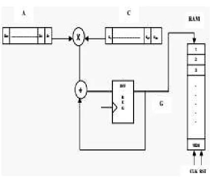
• Accumulating the multiplier output and writing back the results to the output buffers. The input and output buffers are implemented on the FPGA. The matrix-vector multiplications involve multiply and accumulate operations. The multiply-accumulate unit consists of a multiplier and adder. The row and the column elements are supplied as the two inputs to the multiplier.
The output of the multiplier is directly given to the adder as one of the inputs. The previous output of the adder is fed back as the second input to the adder. The multiply-accumulate unit takes each element of the matrix A in row major format and each element of vector C, multiplies them and adds the result to the running total. This process is repeated till the last element of row A and column C. The values are fed in a sequential manner. If the reset signal is asserted high, the contents of registers A and C are cleared.
After a delay, as determined by the implementation results, the first element of vector G is available at the serial output and this output is stored in on-chip memory. This operation is repeated and the process continues until all the rows of matrix A are processed. Finally, the output vector G is available with all the elements stored in the memory locations. A simplified block diagram of matrix-vector multiplication is shown in fig.3.
Fig. 3 Block diagram of matrix-vector multiplication
In order to evaluate the performance of our FPGA-based implementation, the algorithm was coded in VHDL and implemented on Xilinx Virtex-4 (XC4VLX200FF1513, speed grade: -11) family using Xilinx ISE 9.2i tool. The design was synthesized into Virtex-4 FPGA optimized for speed. The hardware resource utilization is summarized in Table 2.
Table 2: FPGA Resource Utilization
As shown in table 2, roughly 14% of the slices and 57% DSP48s are utilized leaving a plenty of room to implement more parallel processors on the same FPGA chip. The results listed in table 2 were obtained using Xilinx ISE 9.2i tool configured to optimize for speed. The total processing time using Virtex-4 FPGA is found to be 58.93 µs; this is equivalent to a throughput of 16970 frames per second. The results indicate the feasibility of using FPGA for real time high speed image processing applications using this matrix-vector multiplication.
Hard ware A rch itectu re
Available online:
https://edupediapublications.org/journals/index.php/IJR/
P a g e | 1804dimensional systolic array based architecture as shown in fig. 4 and fig. 5 for the matrix multiplication.
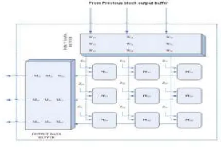
Fig. 4 Architecture of first block
Fig. 5 Architecture of second block
Systolic arrays accelerate medium sized matrix multiplication by exploiting the inherent data parallelism in matrix multiplication. Multiplying the matrix X by the diagonal square matrix Y is equivalent to multiplying the first diagonal element by the entries of first row of X, the second diagonal element by the entries of the second row of X and so on.
Fig. 4 and fig. 5 shows the systolic architecture for both the modules for N1=3 and N2=3 respectively. Both the
matrix multiplier blocks consist of nine identical processing elements, PE1 and PE2, respectively. PE1
consists of multiplier whereas PE2 consists of MAC unit
where each MAC unit consists of a multiplier and adder. The function of each PE1 in the first array is to multiply
the diagonal elements of Y by one element of matrix X during each clock period. First column PE1 are
responsible for producing first column of the product XY referred to as W in the fig. 4, second column generates the second column and so on. The entries are stored in an internal buffer to be used later by the next array. Similarly, the second array as shown in fig. 5 performs the multiplication of (XY) with Z.
Table 3: FPGA Resource Utilization Comparison
IV. CONCLUSIONS
Most of the algorithms which are used in DSP, image and video processing, computer graphics and vision and high performance supercomputing applications have matrix multiplication as the kernel operation. In this paper, we considered two different examples of matrix multiplier architecture where speed is the main constraint. The first design involving computation of dense matrix-vector multiplication is implemented on Xilinx Virtex-4 FPGA and the performance is evaluated by computing its execution time on FPGA. Hardware implementation results demonstrate that it can provide a throughput of 16970 frames per second which is sufficient for many image and video processing applications. The second design for the multiplication of three matrices is based on systolic array and implemented on Spartan-3 and Virtex-II Pro platform FPGAs respectively.
REFERENCES
[1] S. Ogrenci, A. K. Katsaggelos, and M. Sarrafzadeh, “Analysis and FPGA Implementation of Image restoration under resource constraint,” IEEE Trans. on Computers, Vol. 52, No. 3, pp. 390-399, 2003.
[2] C. Ebeling, C. Fisher, G. Xing, M. Shen, and H. Liu, “Implementing an OFDM Receiver on the RaPiD Reconfigurable Architecture,” IEEE Trans. on Computers, Vol. 53, No. 11, pp. 1436-1448, 2004.
[3] G. R. Goslin, “A Guide to Using Field Programmable Gate Arrays for Application-Specific Digital Signal Processing Performance,” M icroelectronics Journal, Vol. 28, Issue 4, pp. 24-35, 1997.
Available online:
https://edupediapublications.org/journals/index.php/IJR/
P a g e | 1805[5] A. G. Ye and D. M. Lewis, “Procedural Texture Mapping on FPGAs,” in Proc. of ACM/SIGDA 7th Intl. Symp. On Field Programmable Gate Arrays, pp. 112-120, 1999.
[6] S. Knapp, “Using Programmable Logic to Accelerate DSP Functions,” http://www. xilinx.com/appnotes/ dspintro.pdf.
[7] J. Ma, “Signal and Image processing via Reconfigurable Computing,” in Proc. of the First Workshop on Information and Systems Technology, 2003.
[8] F. Otto and Z. Pavel, “Hardware Accelerated Imaging Algorithms,” in Proc. of AUTOS’2002 Automatizacesystému, pp. 165-171, 2002.
[9] L. Batina, S. B. Ors, B. Preneel, and J. Vandewalle, “Hardware architectures for public key cryptography,” Integration, the VLSI Journal, Vol. 34, pp. 1-64, 2003.
[10] D. Johnson, K. Gribbon, D. Bailey, and S. Demidenko, “Implementing Digital Signal Processing Algorithm’s in FPGA’s: Digital Spectral Warping,” in Proc. of 9th Electronics