A Novel Design of Cryptography Algorithm for Data Security
using RRG
P.Venkateswara Reddy & B.SudhaKiran
M.Tech(VLSI Design) Dept of E.C.E (VLSI), Lenora College of Engineering, Rampachodavaram, East Godavari, Andhra Pradesh-533288.
AMIETE,M.M.Tech(ES) Associate Professor, Lenora College of Engineering, Rampachodavaram East Godavari, Andhra Pradesh-533288
Abstract—Reversible logic is the recent advancement in the electronics field as it shows low heat dissipating features and low power consumption. On the other hand, reversible logic circuits can decrease energy dissipation theoretically to zero. Recently an approach to encryption/decryption based on using reversible logic circuits has been proposed. This paper presents a solution to designing encryption and decryption schemes based entirely on reversible logic. In our solution a building block of an encryption and decryption scheme is a cascade of 4-input reversible gates. In this way the building block can perform any reversible 4-variable function. For this purpose a reconfigurable reversible gate (RRG) has been proposed. The design of such a reconfigurable gate built from standard reversible gates, i.e. NOT, CNOT, Toffoli and Fredkin gates, is presented. In the paper a complete cryptography scheme for encryption/decryption of 9-bit data is described using Verilog HDL language and its quantum cost is calculated. Simulation and verification of this
Index Terms—encryption, decryption, reversible logic circuits, reconfigurable reversible gate;
I. INTRODUCTION
of circuits built from the NCT library of gates, i.e. NOT, CNOT and Toffoli gates. Modern simulation tools based on FPGAs have enabled modeling of such circuits [11]. The design of a cipher in VHDL was described [9]. In the paper we study an application of reversible logic to developing encryption circuits. The simple implementation of a cipher using reversible circuits was the aim of this work. Each gate used in a cascade of reversible gates is determined by the main key. By choosing different main keys different cascades and different substitution encryption are determined. For this purpose a reconfigurable reversible gate has been proposed. The design of this gate is presented for the first time in the literature. Results of Xilinx ISE based simulation of a simple encryption circuit built from reversible gates are also presented.
The paper is organized as follows. Section 2 recalls basic concepts of reversible logic. In Section 3 design of reconfigurable reversible gate (RRG) is introduced. In Section 4 an implementation of encryption/decryption by cascades of RRG gates is given. In Section 5 simulation of the cipher in Xilinx ISE is presented. Section 6 summarizes the paper.
II. REVERSIBLE DEFINATIONS
Let us recall basic notions of reversible logic gates and circuits.
Definition 1. A completely specified input n-output Boolean function (referred to as n*n function) is called reversible if it maps each input assignment into a unique output assignment. There are 2n ! reversible n*n Boolean functions. For n = 3 this number equals to 40,320, for n = 4 is greater than 2Â1013.
Definition 2. An n-input n-output (n*n) gate (or circuit) is reversible if it realizes an n*n reversible function. In a reversible circuit fanout of each gate output is always equal to 1. As a consequence n*n reversible circuits can be only built as a cascade of k*k reversible gates (k ≤ n).
Definition 3. A set of reversible gates that can be used to build reversible circuits is called a gate library.
Many gate libraries have been examined in the literature. The so called NCT library for n ≤ 4 consists of 1*1 NOT, 2*2 CNOT and 3*3 and 4*4 TOFFOLI gates. Definitions of mixed polarity generalizations of these gates as well as 3*3 Fredkin gate are given below.
Definition 4. Let ai∈{0, 1} for i = 1, 2, 3, 4, and let x' denotes negation of x.
1*1 NOT(x1) gate performs the operation (x1) - (x1 ⊕ 1),
3*3 TOFFOLI(x1, x2, x3) gate performs the operation (x1, x2, x3)- (x1, x2, (x1 ⊕ a1)(x2 ⊕ a2) ⊕ x3),
4*4 TOFFOLI4(x1, x2, x3, x4) gate performs the operation (x1, x2, x3, x4) -(x1, x2, x3, (x1 ⊕ a1)(x2 ⊕ a2)(x3 ⊕ a3) ⊕ x4),
3*3 FREDKIN(x1, x2, x3) gate performs the operation (x1, x2, x3) -(x1, x1' x2 + x1 x3, x1 x2 + x1' x3).
The above defined i*i gates, where i = 1, 2, 3, 4, (in short, denoted by N, C, T, T4 and F, respectively) invert input xi if and only if the values of inputs x1, x2, ..., xi-1 differ from corresponding a1, a2, ..., ai-1 coefficients, passing these inputs unchanged to corresponding outputs. Signals which are passed unchanged from input to output of the gate are called control lines. The signal xi which can be modified by the gate is called target. In the Fredkin gate x1 is the control line. When its input signal is 0 then the signals x2 and x3 are passed to outputs unchanged, and when its input signal is 1 then the signals x2 and x3 are swapped.
Some commonly used names for describing control lines have been introduced. If all a1, a2, ..., ai coefficients equals zero, the gate has positive-polarity control lines. Alternatively, if all a1, a2, ..., ai coefficients equals one, the gate has negativepolarity control lines. These names come
realized by the gate. Positivepolarity means that all inputs which correspond to control lines directly affect the target line. Negative-polarity means that the target line is affected only if the values of control lines are equal to 0. The term mixed-polarity control lines is used if all values of the coefficients a1, a2, ..., ai are allowed to be either 0 or 1. Pictorial symbols of the above defined positive-polarity gates are shown in Fig. 1, and the pictorial symbol of Fredkin gate is shown in Fig. 2.
Fig. 1. Graphical representations of reversible gates N3, C3-1 and T3-210.
Fig. 2. Graphical representation of Fredkin gate F10-2.
F10-2, the first two numbers appearing after the gate’s name (in this example: F) denote controlled (swapping) lines (1 and 0) while the number appearing after the hyphen denotes control line (2). The number of different positive-polarity gates belonging to NCT library which can appear in 4-line circuits is 32 (4 NOT gates, 12 CNOT gates, 12 Toffoli gates and 4 T4 gates).
III. IMPLEMENTATION OF RRG
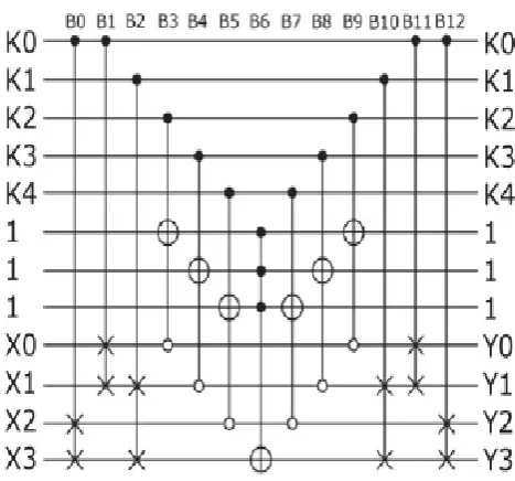
Reconfigurable reversible gate (RRG) replaces one of 32 gates from the NCT library in the cipher. This is why besides 4 inputs transferring information data there have to be five lines for choosing one of 32 types of gates. At the present state-of-the-art of reversible logic synthesis it is not possible to optimally synthesize 9-input reversible gate. After considering many variants of gates RRG the circuit shown in Fig. 3 has been constructed with the relatively small quantum cost equal to 79.
Fig. 3. General scheme of Reconfigurable Reversible Gate (RRG).
The first three Fredkin gates B0, B1 and B2 select the input signal which will be modified by the 4- input Toffoli gate B6. The next three 3-input Toffoli gates B3, B4 and B5 feed control signals for the gate B6 that are selected by the given configuration either input or constant signals. Thus functioning of the gate B6 is determined by signals K. Gates B7, B8 and B9 reconstruct initial constant signals, while gates B10, B11 and B12 fix the order of output signals Y3, Y2, Y1 and Y0. The RRG built from basic reversible gates is shown in Fig. 4.
Fig. 4. Reconfigurable Reversible Gate (RRG).
gate from NCT library have been constructed in VHDL and shown in Tables I and II.
TABLE I. PROCEDURE B_FREDKIN
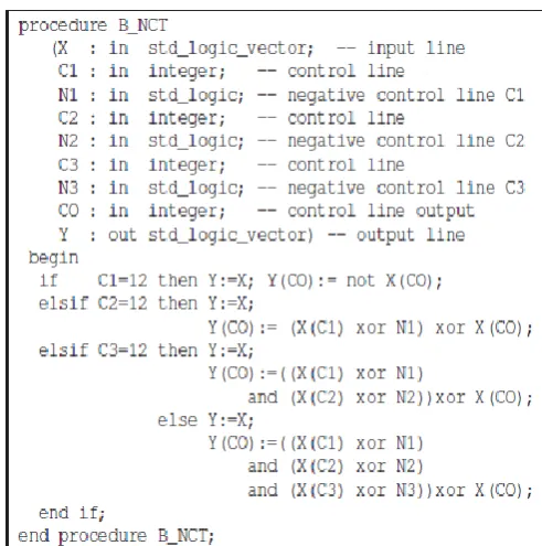
In the procedure B_NCT signals C1, C2 and C3 determine number of line to which control inputs of Toffoli gate are attached while the number of controlled line is determined by signal C0. Binary signals N1, N2 and N3 determine polarization of the control signal Ci. Value N1 = 1 indicates that i-th signal is a negative control signal.
TABLE II. PROCEDURE B_NCT
The above presented procedures were used for describing the gate RRG as shown below.
KX(0):=(KEY(0)&KEY(1)&KEY(2)&KEY(3)& KEY(4) & "111" & DIN(0)&DIN(1)&DIN(2)&DIN(3));
B_FREDKIN (KX( 0),0,10,11, KX( 1)); B_FREDKIN (KX( 1),0, 8, 9, KX( 2));
B_FREDKIN (KX( 2),1, 9,11, KX( 3)); B_NCT (KX(3),2,'0', 8,'1',12,'0', 5,KX( 4));
B_NCT (KX(4),3,'0', 9,'1',12,'0', 6,KX( 5)); B_NCT (KX(5),4,'0',10,'1',12,'0', 7,KX( 6));
B_NCT (KX(6),5,'0', 6,'0', 7,'0',11,KX( 7)); B_NCT (KX(7),4,'0',10,'1',12,'0', 7,KX( 8));
B_FREDKIN (KX(10),1, 9,11, KX(11)); B_FREDKIN (KX(11),0, 8, 9, KX(12));
B_FREDKIN (KX(12),0,10,11, KX(13));
DOUT(3 downto 0)<=(KX(13)(11) & KX(13)(10) & KX(13)(9) & KX(13)(8));
12-bit word KX is the state of line just before or just after gate and is transferred from i-th to (i+1)-th gate.
IV. DESIGN OF ENCRYPTION BY RRG GATE
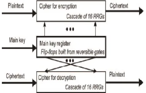
General idea of a cipher built from reversible gates was presented in [9]. It is shown in Fig. 5. The basic element of the cipher is a cascade of 16 4-input reversible gates. The same main key is used for encryption and decryption. The order of gates in the cascade for decryption is reversed in comparison with the cascade for encryption what ensures that it transforms ciphertext into plaintext.
Fig. 5. General idea of a cipher for encryption and decryption built from reversible gates.
It has been proved in [12-13] that optimal circuits for any of the 16! (equal to over 2x10¹³) require at most 15 4-input gates. Thus the circuit shown in Fig. 6 enables realization of any 4-variable reversible function. The circuit has 80 inputs denoted K (with indexes) that are partitioned into groups with 5 inputs in each of them. A 5-line group K[(5*(i+1) – 1):5*i] is used to configure i-th RRG gate. All inputs K are transferred to outputs so they can be reused for controlling the next gate. There are 4 data inputs X[3:0] and three lines with constant inputs (equal to 1) and identical outputs. Detailed description of the main key register as well as the circuit modifying its contents during encryption/decryption are presented in [14].
6. The cascade of reversible gates implementing the 4-bit cipher.
V. SYNTHESIS AND SIMULATION RESULTS
used.In this section, first we will see the synthesis and simulation of the Encryption and Decryption using reconfigurable reversible gate. Encryption and Decryption using reconfigurable reversible gatesare designed on Xilinx ISE 14.7 with Verilog HDL. The RTL schematics and simulation results of the Proposed Reversible Encryption and Decryptions are shown below.
Fig 7. RTL Schematic of Proposed Reversible Encryption
Fig 8. Internal RTL Schematic of Proposed
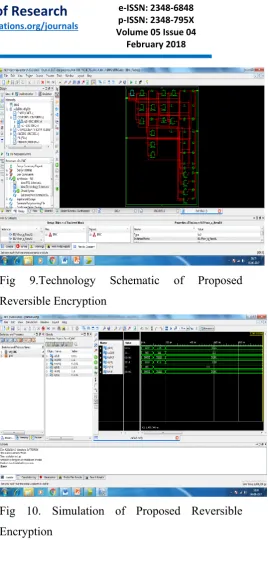
Fig 9.Technology Schematic of Proposed Reversible Encryption
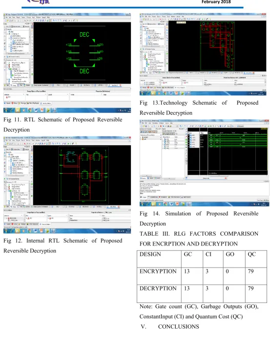
Fig 11. RTL Schematic of Proposed Reversible Decryption
Fig 12. Internal RTL Schematic of Proposed Reversible Decryption
Fig 13.Technology Schematic of Proposed Reversible Decryption
Fig 14. Simulation of Proposed Reversible Decryption
TABLE III. RLG FACTORS COMPARISON FOR ENCRPTION AND DECRYPTION
DESIGN GC CI GO QC
ENCRYPTION 13 3 0 79
DECRYPTION 13 3 0 79
Note: Gate count (GC), Garbage Outputs (GO), ConstantInput (CI) and Quantum Cost (QC)
Firstly we have coded Verilog code for the reversible data encryption and decryption and all the synthesis and simulation results are implemented on Xilinx ISE 14.7. The main aim of the paper is a design of simple reconfigurable reversible gate (RRG) which enables implementation of any of the 32 4-input reversible gates from the NCT library. The design of RRG is presented for the first time in the literature. An application of this gate to implement ciphers for encryption and decryption of binary data is described. Results of encryption and decryption simulation of the cipher built from reversible gates are also presented.
REFERENCES
[1] A. De Vos, Reversible Computing. Fundamentals, Quantum Computing, and Applications. Wiley-VCH, Berlin 2010.
[2] H. Thapliyal and M. Zwolinski,: ―Reversible logic to cryptographic hardware: a new paradigm,‖ Proc. 49th International Midwest Conference on Circuits and Systems, s. 342-346, 2006.
[3] N. M. Nayeem, L. Jamal , and H. M. H. Babu, ―Efficient reversible Montgomery multiplier and its application to hardware cryptography,‖ Journal of Computer Science, vol. 5, no. 1, pp. 49-56, 2009.
[4] Y. Zhang, Z. Guan, and Z. Nie, ―Function
based on reversible logic gates,‖ Proc. International Conference on Multimedia Communications, pp. 104- 107, 2010.
[5] A. Banerjee, ―Reversible cryptographic hardware with optimized quantum cost and delay,‖ Proc. Annual IEEE India Conference, pp. 1- 4, 2010.
[6] K. Datta and I. Sengupta, ―Applications of reversible logic in cryptography and coding theory (Tutorial),‖ Proc. Conference on VLSI Design (VLSID), 2013.
[7] K. Datta, V.Shrivastav, I. Sengupta and H. Rahaman, ―Reversible logic implementation of AES algorithm,‖ Proc. 8th International Conference on Design and Technology of Integrated Systems in Nanoscale Era (DTIS), pp. 140-144, 2013.
[8] A.C. Nuthan, C. Nagaraj and V.B. Havyas, ―Implementation of Data Encryption Standard Using Reversible Gate Logic,‖ International Journal of Soft Computing and Engineering, vol. 3, no. 3, pp. 270- 272, 2013.
[9] A. Skorupski, M. Pawłowski, K. Gracki, and P. Kerntopf, „FPGAbasedmodeling of encryption systems implemented in reversible logic‖ (in Polish), PomiaryAutomatykaKontrola, vol. 58, no. 7, pp. 620-622, 2012.
functions using modeling of gates in FPGA‖ (in Polish), PomiaryAutomatykaKontrola, vol. 60, no. 9, pp. 471-473, 2014.
[11] M. Pawłowski and A. Skorupski, Design of Complex Digital Devices (in Polish), WKŁ, Warsaw 2010.
[12] O. Golubitsky and D. Maslov, ―A study of optimal 4-bit reversible Toffoli circuits and their synthesis,‖ IEEE Transactions on Computers, vol. 61, no. 9, s. 1341-1353, 2012.
[13] M. Szyprowski and P. Kerntopf, ―A Study of Optimal 4-bit Reversible Circuit Synthesis from Mixed-Polarity Toffoli Gates,‖ Proc. 12th IEEE Conference on Nanotechnology, 2012.
[14] M. Bryk, ―Cipher built from reversible gates‖ (in Polish), MSc thesis, Institute of Computer Science, Warsaw University of Technology, February 2016.
Author’s Profile:
P.Venkateswara Reddy received B.Tech from
JNTU Kakinada. Now he is pursuing M. Tech
in Electronics and VLSI Systems at Lenora
College of Engineering, Rampachodavaram,
AP, India.
B.SudhaKiran, AMIETE,M.Tech(ES), currently Working as an Associate Professor, ECE in
Lenora College of