Abstract
GARETTO, ANTHONY DOMINIC. Electron Beam Induced Chemistry. (Under the direction of Dr. Phillip E. Russell.)
The purpose of this research has been to investigate the mechanisms and develop techniques for electron beam induced chemistry. Applications for electron beam
chemistry include repair and fabrication of lithographic masks, integrated circuit repair and rewiring, nanofabrication of functional nanoscale tools and scanned probe
microscopy tips and damage free transmission electron microscope sample preparation. The use of hydrocarbon contamination as a precursor has been investigated and complex three dimensional nanostructures have been successfully fabricated. Accelerating voltage and scan speed can be used to control the morphology of the deposits. The development and implementation of an internal precursor reservoir and introduction device that is transferable to various scanning electron microscope and focused ion beam instruments has been performed. The effects of beam and scan parameters on the
Electron Beam Induced Chemistry
by
Anthony Dominic Garetto
A thesis submitted to the Graduate Faculty of North Carolina State University
in partial fulfillment of the requirements for the Degree of
Master of Science
MATERIALS SCIENCE AND ENGINEERING
Raleigh, North Carolina
2007
APPROVED BY:
________________________________ ________________________________
Dr. Carlton M. Osburn Dr. Dieter P. Griffis
Committee Member Committee Member
Biography
Acknowledgements
I would like to thank the following:
Dr. P. E. Russell, Dr. D. P. Griffis and Dr. C. M. Osburn for their guidance and technical assistance.
Dr. Dale Batchelor, Fred Stevie, Roberto Garcia and Chuck Mooney for their technical assistance and contribution of scientific knowledge.
The Analytical Instrumentation Facility graduate students for their support and assistance.
Dr. Anthony Calamai who worked tirelessly with me as an undergraduate to help me understand and enjoy science.
My love, Dianna, for her support and encouragement and her interest in my work.
Table of Contents
LIST OF TABLES... vi
LIST OF FIGURES... vii
LIST OF ACRONYMS... x
1. INTRODUCTION AND THESIS GOALS ... 1
1.1 INTRODUCTION ... 1
1.2 THESIS GOAL... 2
2. BACKGROUND... 3
2.1 INTRODUCTION ... 3
2.2 APPLICATIONS OF ION AND ELECTRON BEAM CHEMISTRY ... 3
2.2.1 MASK FABRICATION AND REPAIR... 3
2.2.2 ELECTRON BEAM LITHOGRAPHY ... 5
2.2.3 NANOFABRICATION ... 6
2.2.4 TRANSMISSION ELECTRON MICROSCOPY SAMPLE PREPARATION ... 7
2.3 INSTRUMENTATION ... 8
2.3.1 SCANNING ELECTRON MICROSCOPY... 9
2.3.2 ATOMIC FORCE MICROSCOPY ... 12
2.3.3 FOCUSED ION BEAM ... 14
2.4 MECHANISMS OF ELECTRON BEAM INDUCED CHEMISTRY ... 16
2.4.1 PRECURSOR INTRODUCTION OPTIMIZATION ... 17
2.4.2 PHYSICS OF PRECURSOR-SUBSTRATE INTERACTION... 19
2.4.3 BEAM SAMPLE AND BEAM ADSORBATE INTERACTIONS ... 22
2.4.4 EFFECTS OF BEAM AND SCAN PARAMETERS ... 24
2.4.5 PROPOSED MODELS ... 29
2.5 ELECTRON BEAM INDUCED CHEMISTRY ... 31
2.5.1 BEAM INDUCED CONTAMINATION... 31
2.5.2 ELECTRON BEAM INDUCED DEPOSITION ... 34
2.5.3 ELECTRON BEAM INDUCED ETCHING ... 39
2.5.4 COMMERCIAL SYSTEMS ... 43
2.6 FOCUSED ION BEAM INDUCED CHEMISTRY ... 43
2.6.1 FOCUSED ION BEAM CHEMICAL VAPOR DEPOSITION ... 44
2.6.2 CHEMICALLY ENHANCED FOCUSED ION BEAM... 46
2.7 COMPARISON OF ELECTRON/ION BEAM CHEMISTRIES... 47
3. DEPOSITION USING HYDROCARBON CONTAMINATION... 51
3.1 INTRODUCTION ... 51
3.2 EXPERIMENTAL ... 51
3.2.2 DEVELOPMENT OF CONTAMINATION WRITING TECHNIQUE... 53
3.2.3 SCAN SPEED EFFECTS ... 55
3.2.4 ACCELERATING VOLTAGE EFFECTS – BEAM BRANCHING... 57
3.2.5 SUPPLY MECHANISM INVESTIGATION ... 62
3.3 CONCLUSIONS... 70
4. DEVELOPMENT OF PRECURSOR INTRODUCTION METHOD ... 72
4.1 INTRODUCTION ... 72
4.2 INSTRUMENTATION ... 73
4.2.1 HITACHI S-2500 SEM ... 73
4.2.3 PHENANTHRENE PRECURSOR ... 78
4.3 PRECURSOR INTRODUCTION METHOD INVESTIGATION... 81
4.3.1 EXTERNAL VS. INTERNAL RESERVOIR SYSTEM... 82
4.3.2 PRECURSOR FLUX GENERATOR... 89
4.3.3 MODIFIED PRECURSOR FLUX GENERATOR... 92
4.3.4 DEPENDENCE OF DEPOSIT MORPHOLOGY ON VACUUM QUALITY... 94
4.4 CONCLUSIONS... 97
5. EFFECT OF BEAM AND SCAN PARAMETERS ON DEPOSITION EFFICIENCY100 5.1 INTRODUCTION ... 100
5.2 EXPERIMENTAL ... 100
5.2.1 REFRESH TIME AND BEAM CURRENT ... 100
5.2.2 COMPARISON TO FIB-CVD USING PHENANTHRENE PRECURSOR ... 106
5.3 CONCLUSIONS... 110
6. FUTURE WORK ... 111
6.1 TEMPERATURE EFFECT ON DEPOSITION AND REMOVAL... 111
6.2 POST PROCESSING... 111
6.3 EFFECTS OF PARAMETERS ON ALTERNATE PRECURSORS... 112
6.4 EFFECTS OF BEAM AND SCAN PARAMETERS ON DEPOSIT CHARACTERISTICS ... 112
List of Tables
Table 1. Extensive list of precursors used for deposition with an electron beam. The name and formula for each precursor is listed as well as the composition of the
deposit……….. 42 Table 2. Extensive list of precursors used for etching with an electron beam. The name
List of Figures
Figure 1. Schematic diagram depicting a) electron beam induced deposition and b) electron beam induced etching... 16 Figure 2. Schematic diagram of a gas introduction nozzle and substrate including several
relevant parameters. ... 18 Figure 3. Common surface precursor reactions including physisorption, chemisorption,
desorption and surface diffusion... 20 Figure 4. Primary electron beam interaction with sample depicting relevant signals
including backscattered electrons and secondary electrons I and II. ... 23 Figure 5. Schematic diagram showing the relationship between deposition efficiency and
refresh time in arbitrary units. The maximum in deposition efficiency occurs when it is approximately equal to the monolayer formation time (based on model proposed by Koops)... 27 Figure 6. Diagram depicting the interdependent relationship between refresh time and
box size, probe diameter, pixel overlap and dwell time. ... 28 Figure 7. The JEOL JSM 6400F field emission scanning electron microscope used to
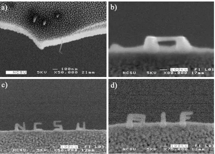
perform the experiments on deposition utilizing hydrocarbon contamination. ... 52 Figure 8. a) Three vertical rods and a lateral scan off the cantilever (image view tilted
slightly from growth orientation). B) Bridge structure, c) NCSU and d) AIF
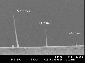
acronyms viewed as grown by manual step lateral scan mode... 55 Figure 9. Carbon rods deposited using line scans of different speed. From right to left
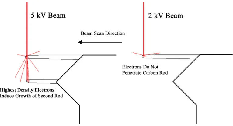
the scan speeds were 80, 320 and 640 s per line at 50,000x corresponding to scan speeds of 44, 11 and 5.5 nm/s. Slower scan speeds generally result in longer thicker rods... 57 Figure 10. Two line scans were performed to deposit the 2 lateral rods as shown in figure a)When tilted to oblique angles as in figures b) (tilted and rotated to show rod 3) and c) (top down view) we can see that one line scan actually grew two rods due to forward scattering of electrons... 58 Figure 11. Electron Flight Simulator Monte Carlo Simulations for a) 5kV beam and b)
2kV beam in a C rod. The 5 kV beam easily penetrates the 150 nm diameter C rod while the interaction volume for the 2 kV beam is almost entirely contained within the C rod... 59 Figure 12. Growth of more than one rod by a single scan of a 5 kV beam is depicted. As
the beam is scanned from right to left a second rod is deposited behind the first where the highest density of forward scattered electrons hits the substrate. A 2 kV beam does not penetrate the C rod... 60 Figure 13. Images of the depositions performed at 2 kV and 5 kV shown a) as grown, b)
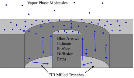
top down and oblique angle views illustrating the uniformity of the 2 kV structure and c) spurious growth and d) multiple, unintended rods grown with the 5 kV beam. ... 61 Figure 14. Structure grown by laterally depositing 4 rods off the cantilever edge and
indicate the surface diffusion path down and across the trench and up the central pillar. ... 64 Figure 16. Two FIB milled trenches demonstrating the effects of machine time on the
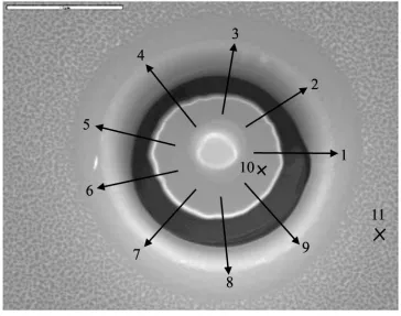
pillar morphology. The first pattern superimposed circle 1 for 10 min and circle 2 for 10 min while the second pattern superimposed circle 1 for 10 min and circle 2 for 20 min... 66 Figure 17. Numbered arrows 1-9 indicate the position and orientation of the 9 laterally
grown rods. The vertical rods deposited using spot mode are indicated by x’s
labeled 10 (on pillar) and 11 (outside trench)... 67 Figure 18. FIB Pillar with 9 lateral rods scanned off the center. The vertical rods grown
in spot mode can be seen on the upper right of the pillar and above the trench on the gold coated silicon substrate. ... 68 Figure 19. Micrographs of rods grown in spot mode off the central pillar and away from
the trench. Volume calculation formulas are shown... 69 Figure 20. Schematic diagram showing the basic electron beam chemistry setup with an
external reservoir. The flow valve is used to start and stop the flow of precursor vapor which enters the vacuum chamber along the conductive path and is introduced to the substrate via the nozzle. ... 73 Figure 21. Hitachi S-2500 equipped with a turbopump and beam scan generator shown
on the right. The external reservoir can be seen protruding from the right side of the chamber... 76 Figure 22. Screenshot of beam pattern generator software. Up to 10 boxes can be
defined in the white area with beam and scan parameter inputs to the left. Image acquisition options are on the right... 77 Figure 23. Schematic of a phenanthrene molecule (C14H10) consisting of three fused
benzene rings. ... 79 Figure 24. Mass spectrum for phenanthrene showing the primary peak at 178. ... 79 Figure 25. Dissociation cross-section for phenanthrene as calculated by the author
utilizing the method proposed by Alman... 81 Figure 26. Schematic diagram of the constructed external reservoir system. The
phenanthrene is placed in a glass reservoir and is inserted into brass tubing filled with sand. Set screws are used to mechanically stabilize the reservoir... 83 Figure 27. External precursor reservoir system consists of a) reservoir, piping wrapped
with heating tape and control valves on the outside. B) Teflon tubing leading to a hypodermic needle aimed at the substrate surface... 83 Figure 28. Proof of concept internal reservoir system used for comparison to external
reservoir system. a) The system was constructed on a 4” SEM sample holder. B) A closer image showing the Faraday cup for beam measurements and Cu grid for focus and stigmation... 85 Figure 29. Four box pattern used for external vs. internal reservoir system deposition
efficiency comparison. The right shows a typical SEM micrograph of the resulting deposit. The deposits are about 50 µm from the Au layer... 87 Figure 30. Deposition efficiency of external and internal reservoir system. For all boxes
Figure 31. a) PFG components disassembled. B) Top view of assembled PFG with Faraday Cup and copper grid and a c) side view of diagram and actual PFG depicting reservoir of phenanthrene and four conductive pathways leading to
hypodermic needles aimed at substrate surface... 90 Figure 32. Schematic diagram of machined PFG. Precursor sits in the reservoir below
the sample substrate and the vapor flow through the four conductive paths and is introduced to the sample surface... 92 Figure 33. Modified PFG shown dissassembled above and the steps for assembly below. 1) Precursor reservoir, 2) spacer, 3) sample puck and 4) introduction head. ... 93 Figure 34. Assembled PFG with a Faraday Cup added for beam current measurements
and a Si sample on the sample puck. ... 93 Figure 35. Mass sweep spectra showing the species present during the deposition of
three boxes at different times after pumpout. The black trendline is immediately after pumpout, the green one hour after, and the red 6 hours after... 96 Figure 36. AFM data of deposits performed at pumpout, 1 hour after pumpout and 6
hours after pumpout. Top down, thermal scale height images and individual line scans taken fronm the indicated location across the deposits ... 97 Figure 37. Chart summarizing the benefits and drawbacks of the different precursor
introduction methods in this work. ... 99 Figure 38. Seven box pattern with box size and total exposure time proportionally
changed in order to vary refresh time while holding all other parameters constant. ... 102 Figure 39. AFM images used to obtain volume of deposited boxes. Typical scans for a)
20 by 20 µm2, b) 7 by 7 µm2 and c) 1 by 1 µm2. Note the z scale is the same but the x-y axes are scaled to the box size. ... 103 Figure 40. Deposition efficiency versus refresh time for depositions performed at 20 pA
and 100 pA using the PFG. Deposition efficiency increases for long refresh times and low beam currents. ... 104 Figure 41. Deposition efficiency plotted as a function of refresh time. Refresh time was
varied by changing the dwell time. ... 105 Figure 42. Deposition efficiency versus refresh time varied by changing both box size
and dwell time... 106 Figure 43. Hitachi FB2100 FIB system equipped with a Ga ion beam, SEM and TEM
sample introduction chambers. PFG was modified to be inserted into the SEM stage in order to perform FIB-CVD with a phenanthrene precursor. ... 107 Figure 44. PFG modified with dovetail mount for insertion into Hitachi FB2100 FIB
system. ... 108 Figure 45. 3 Dimensional AFM reconstructions of electron beam and ion beam
List of Acronyms
AFM – Atomic Force Microscope
AIF – Analytical Instrumentation Facility BSE – Backscattered Electrons
CE-FIB – Chemically Enhanced Focused Ion Beam CL – Cathodoluminescence
EB – Electron Beam
EBID – Electron Beam Induced Deposition EELS – Electron Energy Loss Spectroscopy EUV – Extreme Ultra-Violet
FIB – Focused Ion Beam
FIB-CVD – Focused Ion Beam Chemical Vapor Deposition IC – Integrated Ciruit
MEMS – Microelectromechanical System NCSU – North Carolina State University NEMS – Nanoelectromechanical System PE – Primary Electrons
PFG – Precursor Flux Generator SE – Secondary Electrons
Chapter 1. Introduction and Thesis Goals
1.1 Introduction
The continuous demand for smaller integrated circuit (IC) chip feature size as well as the need for a consistent, high resolution technique for nanofabrication of functional 3 dimensional structures and devices has spurred the interest in both focused ion beam and electron beam induced chemistries. The realization of ultra large scale integration (ULSI) has increased the number of devices per chip to over 1,000,000, increasing the chip size and calling for a higher resolution technique to reduce device size. High resolution and easily controllable direct write techniques are necessary for the deposition of 3-dimensional microelectromechanical systems (MEMS),
nanoelectromechanical systems (NEMS) and functional nano-tools useful for the advancement of nanotechnology and biomedical applications. Advancing analytical techniques such as transmission electron microscopy (TEM) have very stringent sample preparation requirements including sample thicknesses under 100 nm and low defect densities.
Focused ion beam (FIB) and electron beam (EB) induced chemistry techniques are very viable options for all of these applications due to their high spatial resolution capabilities. FIB systems are most commonly used for many of these applications because the large mass of the gallium ions can physically sputter away surface material. The addition of a properly chosen precursor to the local beam impingement area can enhance the etch rate, improve selectivity or allow for deposition of a desired material.
Some of the applications for these machining methods include mask repair of both clear and opaque defects, integrated circuit (IC) repair and modification1, semiconductor laser fabrication, microelectromechanical systems (MEMS)2 and nanoelectromechanical systems (NEMS)3 devices, TEM sample preparation4 and most recently, fabrication of functional 3-dimensional nano-tools for biomedical and other applications.
1.2 Thesis Goal
Chapter 2. Background
2.1 Introduction
This chapter presents an overview of the basic concepts and technologies required for this work. Applications for electron beam chemistry are reviewed including
lithography and nanofabrication techniques that are employed today as well as their advantages and disadvantages making electron beam chemistry a viable alternative. The fundamental concepts of relevant techniques such as scanning electron microscopy (SEM), atomic force microscopy (AFM) and focused ion beam (FIB) are discussed. The mechanisms behind the beam induced chemistry process are addressed and supported by experimental evidence. A thorough literature review of both electron beam and focused ion beam chemistry are presented as well as a collective study of previous precursor gases reported.
2.2 Applications of Ion and Electron Beam Chemistry
A wide variety of applications exist for EB induced chemistry due to the high resolution, low damage and precise control of the process. Commonly used lithography and nanofabrication techniques are addressed in the following sections. The relevance of EB induced chemistry to these techniques are addressed along with the reasons that EB induced chemistry is such a promising method.
Possible applications such as mask repair, lithography, nanofabrication and TEM sample preparation are addressed.
2.2.1 Mask Fabrication and Repair
projection printing such that exposure of an entire wafer requires a step and repeat process.
X-ray lithography7 is a promising method for the reduction of feature size. It is similar to optical proximity printing but the mask to wafer distance and feature resolution can be increased. X-ray lithography systems use x-rays with energies in the range of 1-10 keV, corresponding to wavelengths on the order of 1 nm. Diffraction effects are therefore negligible and high resolution features under 0.1 µm are easily attained.
Because significant areas can be exposed using a step and repeat method their throughput is comparable to that of current optical exposure systems.
X-ray lithography is limited by issues associated with the masks, among others. The clear areas of the mask must be transparent to the 1 nm x-rays meaning they must be made of a low mass material (Si, Si3N4 and SiC are common) and be very thin (less than a few µm thick). The opaque regions are typically made from gold or tungsten as they absorb x-rays. Therefore these masks are very fragile and have rigorous manufacturing requirements. They are typically fabricated by spinning a photoresist on the absorber layer and using direct write e-beam lithography to pattern the mask. EB chemistry is a very promising application for the repair of x-ray masks9.
Extreme ultra-violet (EUV) lithography uses photon energies around 100 eV corresponding to wavelengths between 10 and 15 nm10. These wavelengths can be considered at the low energy end of the x-ray spectrum (soft x-rays) or at the high end of EUV. The idea is to extend the projection lithography principles into this regime through the use of high-reflectivity EUV mirrors (reflective masks) rather than transmissive masks since photons of this wavelength are readily absorbed. The entire exposure system including the mask and reducing optics is composed of curved multilayered mirrors often consisting of alternating silicon/molybdenum multilayers. Problems that must be
overcome are issues associated with the fabrication and repair of defects in the aspheric mirrors and masks11 and the need for a reliable, cost-effective laser-driver.
results in unacceptable alterations in the optical properties of the structural quartz substrates onto which the masking layers are applied12. Introduction of a gaseous precursor can be used to increase the etch rate and decrease both Ga implantation and redeposition. Use of a FIB and the proper precursor(s) to repair defects can result in transmittances of 95% or better13. The use of Ebs for mask repair allows higher resolution than FIB and a reduction in damage. The ability to form probe sizes well under 10 nm with an EB allows high resolution. Elimination of the deleterious effects of FIB makes EB induced chemistry a very attractive method for mask fabrication and repair. Use of an electron beam to repair clear and opaque defects has been demonstrated by Edinger et al14.
One of the major costs associated with the lithographic process is mask
fabrication. Due to this expense and the stringent fabrication requirements placed on the mask the need exists for a method that allows not only fabrication but repair of both clear and opaque defects as well. If the mask problems associated with x-ray or EUV can be overcome then these systems may provide an option for the next generation of
lithography. EB induced chemistry presents a viable option for the fabrication and repair of these masks because of the ability to directly deposit or remove material with high resolution and high precision. The ability to perform repair without significantly altering the optical properties makes the repair of both clear and opaque defects possible.
2.2.2 Electron Beam Lithography
resists include SAL601 (Shipley Co.)15, poly methyl methacrylate16,17 and calixarene18,19 and its derivatives20.
The major drawback of EB lithography is the low throughput compared to other lithographic methods. Current optical lithographic techniques obtain throughputs on the order of 60 wafers/hour for 200 mm or 300 mm wafers. The EB throughput limitation arises because of the need to scan over the desired area. Each pixel must be irradiated with the focused beam which which means the beam must be scanned at a speed that allows for chemical modification of each pixel. At high beam intensities the resolution is degraded due to the coulomb interaction between the electrons in the beam. Many groups have addressed the low throughput issue in different manners, the most common being the development of multiple beam systems21,22 23 24, , .
The direct-write capabilities of EB induced chemistry provide a major benefit for specialty applications over conventional resist based techniques due to the elimination of the pre and post-exposure steps. Adsorbed gas molecules are irradiated to induce the chemical reaction so there is no need for a resist layer. This eliminates the cost and time associated with both application of the resist as well as post exposure steps required to remove the exposed or unexposed regions. The limiting factor arises from the need to irradiate every pixel with the focused beam which leads to a low throughput compared to conventional methods.
2.2.3 Nanofabrication
Nanofabrication is defined by the American Heritage Dictionary as “any
technique used to create objects or mechanisms on the scale of nanotechnology”25. This scale refers to dimensions less than 100 nm and is of paramount importance for the advancement of the semiconductor field, bio-medical applications,
nanoelectromechanical system (NEMS) devices, and microelectronics26.
Nanofabrication deals not only with the fabrication of nano-objects but also with the patterning of substrates and thin films on this scale.
field methods (supramolecular assembly, monolayer self-assembly, directed self
assembly, nanoparticle formation and probe lithography). These bottom-up methods will be not be addressed in this work.
Top-down techniques originate from solid state physics and are based on the continuous reduction of dimensions including lithography, micromachining and
deposition with energetic beams. The only top-down techniques that will be covered here are FIB and EB direct write methods.
FIB systems have been used for nanofabrication since the mid 1980’s because they induce many useful processes for deposition 28,29 and material removal30. Matsui et al. have utilized focused ion beam chemical vapor deposition (FIB-CVD) to fabricate functional nano-tools such as a nano-net31, nano-actuator and nano-manipulator32 using a phenanthrene precursor. They have experimentally demonstrated that the nano-tools are potentially very useful for cell operations and analysis in bio-experiments. Focused ion beam chemical vapor deposition (FIB-CVD)33,34 is a flexible technique for
nanofabrication allowing for the deposition of various materials.
Utilization of an EB eliminates Ga implantation and physical sputtering due to the small mass of an electron. A precursor is required for both etching and deposition. The rate for EB is slower than for FIB, but the damage to the sample is negligible compared to FIB35. EB induced chemistry may be a useful method for both device fabrication and TEM sample preparation where beam induced damage is unacceptable36.
FIB and EB induced chemistry are both important techniques for the fabrication of objects on the nanometer scale because of their direct write capabilities, resolution, and precise control. While the throughput for both techniques limit their use in large scale manufacturing tasks at this time, each method has its own benefits and limitations which will be described in detail in later sections.
2.2.4 Transmission Electron Microscopy Sample Preparation
much effort put toward making the sample preparation methods easier and improving sample quality37.
In order to reach electron transparency the sample is usually thinned to well under 100 nm. This thickness can be obtained by several methods including grinding and polishing, mechanically dimpling, microtome or using a low angle ion-mill. Most recently the use of FIB has been employed to perform lift out TEM samples in which a thinned sample is cut out of a substrate, removed and attached to a TEM specimen grid. The method is performed completely in-situ in the FIB and an experienced operator can obtain reproducible sample thicknesses. With today’s instruments TEM samples can be prepared on the order of an hour38.
Despite the throughput increase over traditional methods, sample damage from FIB is a problem that effectively degrades TEM resolution. Among these are ion implantation, redeposition, amorphization and surface roughness39. Damage layers of 20-30 nm are typically obtained for a 30 kV FIB40. This damage can be reduced in many ways such as the use of a low energy FIB for polishing41, post-lift-out etching or gas assisted etching.
EB induced etching is one possible solution for the preparation of near damage-free TEM samples. Due to the small mass of the electron there is no physical sputtering component and no ion implantation associated with EB induced etching. However, because there is no physical sputtering, the removal rate is much slower for EB induced etching than with FIB induced etching, making it unrealistic to perform an entire TEM liftout with EB induced etching alone. Using EB induced etching to polish off damage sustained during a lift-out technique using FIB is one possibility. The recent advent of dual-beam systems makes this a very feasible option.
2.3 Instrumentation
2.3.1 Scanning Electron Microscopy
The first SEM was constructed by von Ardenne in 1938 by raster scanning the beam in a TEM42. In 1951 at the Cambridge University Engineering Laboratory the first modern day SEM was constructed by D. McMullan43. Today’s SEM can obtain sub-nanometer resolution and is considered essential for analytical characterization and microscopy.
A typical scanning electron microscope consists of a vacuum chamber, an electron source, a column and various detectors. The vacuum system consists of one or more separately pumped regions. The first region houses the source and optics and requires a vacuum of 10-6 torr to 10-9 torr depending on the source. In the case of a W or LaB6 thermionic source a lower vacuum is required than for a field emission source. This region is responsible for the production and formation of the electron probe. In some systems the source region is pumped separately from the optics resulting in three separately pumped vacuum regions.
The second region is the sample chamber typically held in the 10-6 torr range and is often pumped by the same system. Separation by a pressure limiting aperture may be used if the source has higher vacuum requirements. A mechanical roughing pump backing a turbomolecular pump or an oil diffusion pump is commonly used. In some instruments a separate sample introduction chamber is utilized so the vacuum to the main chamber does not have to be broken every time a sample exchange is performed.
Electrons in an SEM are produced thermionically or by field emission.
Thermionic emission occurs when a current is applied to a cathode under vacuum so that the electrons of the cathode can overcome the work function by thermionic excitation.
Typical thermionic emitters are made of tungsten (φ=4.5 eV, TM= 3643 K) or lanthanum
hexaboride (φ=2.5 eV,TM= 2800 K). These materials are chosen because of their low work functions, high melting temperatures and stability in mild vacuums. Tungsten emitters are bent into a hairpin or milled to a sharp tip while in the case of LaB6, single crystal rods are polished to a point. This is important to concentrate the electric field to the tip making extraction easier and providing a smaller source.
resulting in a high electric field at the tip which lowers the potential barrier allowing electrons to tunnel through and leave the tip. Field emission cathodes consists of fine wire tips (<100 nm) typically made from tungsten which can be heated to avoid gas adsorption and increase stability or can be operated at room temperature. Their main advantages are significantly higher gun brightness, smaller spot size and a small energy spread.
Electrons produced either thermionically or by field emission are directed down the column of the SEM with an amount of energy referred to as the accelerating voltage. This is accomplished by applying a high voltage across the cathode and anode, typically in the range of 1-30 kV. Higher accelerating voltages provide a smaller obtainable spot size and are preferable for high resolution imaging. Lower accelerating voltages produce a smaller interaction volume which provides more surface information and less beam induced damage.
Electron lenses are used to demagnify the initial spot size into the small final probe diameter dp on the specimen. Electromagnetic lenses are converging lenses that are rotationally symmetric. Consisting of a coil of wire enclosed in an iron case, when a current is applied to the wire, fringing magnetic field lines in an axially symmetric fashion interact with the accelerated beam of electrons. These magnetic fields push off-axis electrons closer to the optic off-axis reducing the effective spot size. Typical SEMs have one to three condenser lenses used to demagnify the beam diameter.
To further control the spot size, beam limiting apertures are employed to limit the convergence angle of the beam. Off axis electrons are blocked which also reduces spherical aberration. A final objective lens focuses the probe of electrons on the sample surface and contributes to reducing the spot size.
before returning back to the original pixel. The time it takes for the beam to make one complete sweep and return back to the initial pixel is called the refresh time, τR.
Dose is defined as the total number of electrons or charge deposited in the irradiated area and is given by the equation44
A t i
D= b × (1)
where ib is the probe current usually expressed in the range of pA to nA and t is the total time the defined area is exposed to the beam in seconds. This value is expressed in units of electrons per square nanometer [e-/nm2] or more commonly reported as
microcoulombs per square centimeter [µC/cm2].
As the primary beam electrons enter the specimen they interact with the electric fields of the substrate atoms. This interaction can deflect the beam electrons along a new trajectory with no kinetic energy loss, a process called elastic scattering. These types of collisions cause forward and lateral spreading resulting in a large interaction volume that can be several microns. If several of these scattering events occur or a single high angle event, primary beam electrons can exit the sample surface as a backscattered electron (BSE). The probability of elastic scattering is defined as the cross section for elastic scattering Q, and can be calculated using the following equation44
⎟ ⎠ ⎞ ⎜ ⎝ ⎛ ⎟⎟ ⎠ ⎞ ⎜⎜ ⎝ ⎛ × = − 2 cot 10 62 . 1 2 2 2 20 o E Z
Q φ (2)
This equation gives the probability of an elastic scattering event occurring at angles greater than the specified angle φo [degrees or radians] for electrons with energy E [eV] hitting a sample of atomic number Z. Using this cross section and the density of the sample ρ in g/cm3, the mean free path or distance between scattered events in the sample can be calculated by44
Q N
A
oρ
λ= (3)
Another type of interaction, inelastic collisions, occurs when the incident beam interacts with the specimen. During inelastic collisions, beam electrons lose energy to the specimen atoms or electrons with little or no change in trajectory. Inelastic scattering events result in the production of many signals from the sample including secondary electrons, x-ray photons, phonons, auger electrons and cathodoluminescence (CL). Secondary electrons are very useful and are the most commonly used signal for imaging in SEM. Secondary electrons are ejected from the sample due to the impingement of primary beam electrons and are historically defined as having an energy of 50 eV or below44.
X-ray photons are another useful signal that can give both qualitative and
quantitative information about composition. As the primary beam deposits energy to the substrate atoms, ground state electrons can be excited to higher energy orbitals. These electrons then return to their ground state emitting an x-ray with an energy characteristic of that atom. These x-rays can then be collected and sorted by energy or wavelength in order to determine the composition of the specimen.
As the beam is rastered over the defined area by electromagnetic scan coils signals are emitted from each point that is irradiated. The desired signal is collected with the appropriate detector at each point and an intensity value is assigned to a
corresponding pixel on the display. This yields an image where each pixel position corresponds to an x-y position of the beam and intensity level represents the amount of collected signal.
2.3.2 Atomic Force Microscopy
Atomic force microscopy (AFM) is one of many specific techniques in a class of microscopy known as scanned probe microscopy (SPM). SPM techniques utilize a small physical probe that is brought in close proximity to the sample and scanned across the surface in order to obtain spatially resolved information of a specific surface interaction or property. The acquired information is recorded for each x and y location and used to construct a three-dimensional map of the specific interaction or property.
construct an image which allows insulators and conductors to be imaged
non-destructively. AFM utilizes a small probe mounted on the end of a cantilever to measure changes in topography due to interatomic and intermolecular forces.
The tip acts as a force sensor defined by Hooke’s Law in which the force, F in the range of nN to μN, causing a deflection of magnitude x on the cantilever with a spring constant of k in N/m has a magnitude of45
x k
F = ×δ (4)
Typically made of Si3N4 or Si, the tip is scanned across the sample surface and sub-angstrom changes in topography deflect the cantilever.
These deflections are registered by a solid state laser reflected off the backside of the cantilever and detected by a position sensitive photo detector (PSPD), generally consisting of two photodiodes. The magnitude of the deflection from the tip/sample interactions is used as a feedback mechanism in order to maintain a constant force between the tip and sample.
A piezoelectric tube scanner is typically employed for x, y and z motion of the tip and sample with respect to each other. Piezoelectric materials expand or contract
proportionally to an applied voltage depending on the polarity. The scanner incorporates four or six independently operated piezo electrodes for x,y and z motion into a single tube. This results in a scanner that can manipulate probes with extreme precision and sensitivity in all three dimensions. Some models of AFM move the sample with respect to the tip while some move the tip with respect to the sample. The z motion of the
scanner is used as a feedback mechanism to maintain constant height, force or oscillation amplitude depending on the mode of choice.
non-contact will not be addressed in this work as the method employed for measurements was TappingMode ™ AFM.
In TappingMode™ AFM the cantilever is oscillated slightly below its resonance frequency with the tip lightly contacting the sample surface at the bottom of each swing. The amplitude of oscillation is typically 20 to 100 nm and the feedback loop moves the vertical position of the scanner to maintain a constant root mean square (RMS)
amplitude. The vertical position of the scanner is recorded and used to construct a topographic image.
The use of AFMs are commonplace for surface characterization and can provide a wealth of information alone or when used in conjunction with other techniques such as SEM, x-ray photon spectroscopy (XPS), and secondary ion mass spectroscopy (SIMS). The absence of tedious sample preparation and the ability to achieve sub-atomic
resolution in ambient conditions make the use of AFM all the more attractive. Virtually any sample can be imaged including conducting and insulating materials as well as some biological samples in a non-destructive manner.
2.3.3 Focused Ion Beam
Focused ion beams have been in use since the 1960’s46,47 for isotopic and compositional characterization of minerals in which ions are sputtered off of a sample and guided by electrical fields to a mass spectrometer where they are collected and analyzed. The first liquid metal ion source (LMIS) utilized with focusing optics was constructed by Seliger et al48 in 1979. Immediately following this several groups developed their own FIB systems49 that utilized a finely focused beam of ions in a fashion similar to a scanning electron microscope50. The beam is rastered over a desired area in order to produce an image via collected secondary ions or electrons, or to
micromachine materials.
The basic FIB system consists of a vacuum system, liquid metal ion source (LMIS), ion column and sample chamber, which is also held under vacuum, and detectors. It is very similar to modern day SEMs except for the use of an ion beam instead of an electron beam.
region containing the LMIS. A turbomolecular pump (TMP) backed by a mechanical forepump is often used for the sample introduction and main sample chambers. Pressures in the 10-6 or 10-7 torr range are possible with this setup and are sufficient to increase the mean free path of the ions allowing them to reach the sample before scattering. The source and column must be under higher vacuum to avoid contamination of the source and prevent electrical discharges. Ion pumps are usually used which can reach vacuum pressures of 10-8 to 10-9 torr and the column and source are separated from the main chamber by a pressure limiting aperture.
The LMIS in a FIB is most commonly a fine tip tungsten wire attached to a reservoir with the metal source material. Ga is typically used for a number of reasons including its low melting temperature (29.8 C), low volatility, low vapor pressure and excellent vacuum properties among others. The Ga is heated causing it to flow and wet the tungsten wire. An applied electric field on the order of 108 V/cm causes the liquid Ga to form a point source (known as a Taylor Cone). Ga is pulled from the tip by an
extraction voltage and ionized by field evaporation of the metal.
Once the Ga ions are extracted from the LMIS, a 5-40 kV potential accelerates them down the column. Two lenses are typical in a FIB, a single condenser lens and an objective lens. The condenser lens is responsible for the formation of the probe while the objective lens is used to focus the probe on the sample. There are also beam limiting apertures, similar to those of an SEM, which help define the spot size and reduce off axis ions. Stigmation and beam deflection are performed with octupole deflectors and a beam blanker is included to reduce damage to the surface when possible.
Unlike electrons in the SEM, ions are destructive to the sample and can be used to physically mill small features by sputtering away substrate atoms. Gallium has a large atomic mass of 69.72 amu which causes a number of events when focused onto a sample at such a high acceleration voltage. Elastic collisions occur resulting in the sputtering of atoms and ions from the sample, while inelastic collisions produce ejected secondary electrons, x-rays, photons and phonons.
systems are used extensively in the semiconductor industry and materials science for many applications including failure analysis and microscopy, cross-sectional sample preparation, TEM sample preparation and nanofabrication38.
2.4 Mechanisms of Electron Beam Induced Chemistry
The basic concepts of beam induced chemistry involve the interaction of a particle beam incident with adsorbed molecules on the surface of a substrate. A gas phase
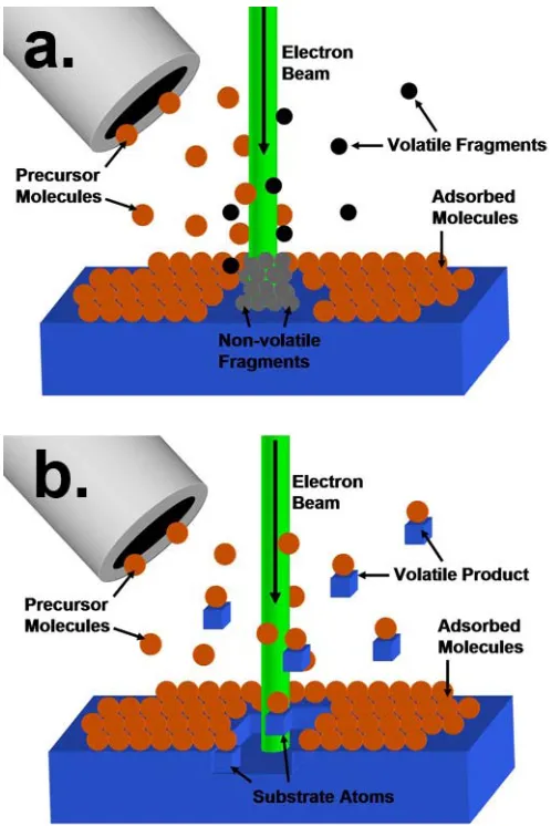
precursor is locally introduced to the substrate and adsorbs to the surface. Upon irradiation with an electron beam a chemical reaction occurs as depicted in Figure 1. Deposition occurs when the decomposition products are non-volatile and material removal occurs when the reaction products are volatile.
The following sections provide an in depth discussion of the process and a
description of the mechanisms that govern precursor introduction, beam sample and beam precursor interactions and the effects of beam and scan parameters. An in depth literature review is presented beginning with beam induced contamination and following the
development of EB induced chemistry process. Precursors used and results found by several groups are discussed and models proposed by others are presented.
2.4.1 Precursor Introduction Optimization
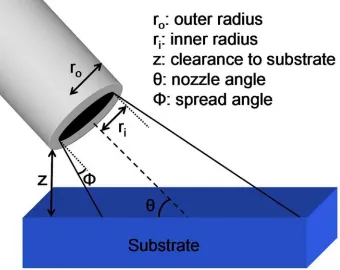
Figure 2. Schematic diagram of a gas introduction nozzle and substrate including several relevant parameters.
The molecular flux is controlled by the dimensions of the needle and its
orientation with respect to the sample as well as the temperature of the reservoir and any valves or limiting apertures. These parameters must be optimized for the maximum and most uniform precursor delivery rate52. The optimum gas flux is obtained when the projected gas area is minimized resulting in the highest density of molecules per unit area. For a given precursor flow rate, this can be obtained by a short nozzle to substrate distance (z), a low spread angle (Ф, dependent on length/diameter ratio of nozzle), small nozzle radius (ri) and a nozzle angle (θ) approaching 90 degrees to the substrate surface. These parameters are depicted schematically in Figure 2.
respect to the substrate normal is undesirable as it results in a change in the spatial distribution of Ses due to forward scattering.
After optimization of the nozzle-substrate geometry, the molecular flux can be further increased by raising the temperature of the precursor reservoir. As the
temperature of the reservoir is increased, the vapor pressure of the precursor in the reservoir increases as well. This causes more molecules to flow through the introduction nozzle and raises the local pressure at the substrate surface. The arrival rate or flux of molecules at the surface is directly proportional to the local pressure at the surface. The flux of molecules in mol/m2 s, defined by the kinetic theory of gas is given by53
mkT p F
π
2
= (5)
where p is the local pressure in Pascal, m is the molecular mass in kg, k is Boltzmann’s constant (1.38×10⁻²³ J/atom-K or 8.62×10⁻⁵ eV/atom-K) and T is the temperature of the substrate surface in Kelvin. Heating of the conductive path to the introduction nozzle is required in some cases to hinder condensation of precursor molecules along the pathway.
In the case of very high precursor introduction rate in relation to the pumping speed of the system, the molecular flow must be restricted. If the local pressure above the surface of the substrate exceeds the 10-3 torr regime, significant scattering of primary beam electrons occurs. The molecular flow can be restricted by the installment of flow restricting valves along the conductive pathway. Needle valves can be used to restrict and adjust precursor flow while a second valve can be used to turn the flow on and off when necessary without altering the flow valve setting thus changing the precursor flux between experiments.
2.4.2 Physics of Precursor-Substrate Interaction
When a flux of molecules impinges on the sample surface the molecules will adsorb with some probability known as the sticking coefficient, s, which determines the adsorption rate. There is a linear relationship between the adsorption rate, Rads, and the sticking coefficient given by54
sF dt
dN R ads
where Rads is the adsorption rate in molecules/m2s, Nads is the number of adsorbed molecules in molecules/m2, t is the unit of time in seconds, F is the initial surface flux in molecules/m2s and s is the sticking coefficient which is unitless.
The sticking coefficient is assigned a value between 0 and 1. A value of 1 means every molecule that impinges on the surface will adsorb while a value of 0 means that no impinging molecules will adsorb. The sticking coefficient depends upon the specific chemistry and physics of the surface, the chemical characteristics of the precursor, surface coverage and temperature. The sticking coefficient is given by the equation53
kT Ea
e f s
− ⋅
= (θ) (7)
where f(θ) is a function of the existing surface coverage of the adsorbed species, Ea is the activation energy of adsorption in eV, k is Boltzmann’s constant, and T is the temperature of the solid interface in Kelvin. Knowledge of the actual sticking coefficient values is not well known for most molecules and a value of 1 is often assumed to simplify models.
Figure 3. Common surface precursor reactions including physisorption, chemisorption, desorption and surface diffusion55.
substrate atoms and adsorbed precursor atoms. Chemisorption is the stronger of the two mechanisms with energies in the range of 1-10 eV/atom.
Physisorption on the other hand, is a weaker non-chemical bond due largely to the Van der Waals forces arising from dipole moments. The chemical identity of the
adsorbate remains the same and typical energies for this type of bond are in the 50-500 meV/atom range. Figure 3 depicts both physisorption and chemisorption along with other common surface-precursor reactions including desorption and surface diffusion. The amount of time an adsorbed molecule remains on the surface before
desorption is referred to as residence or mean stay time. Residence time is also inversely proportional to the surface temperature and is given by56
⎟ ⎠ ⎞ ⎜ ⎝ ⎛ =
kT E t
tR oexp des (8)
where to is the pre-exponential factor [seconds] and Edes is the activation energy for desorption of the adsorbed molecule [eV]. Therefore lowering the substrate temperature results in a longer average residence time for each molecule. If the residence time is increased adsorbed molecules remain on the surface for longer time leading to a higher concentration of adsorbed molecules. Heating the specimen results in lowering the supply rate as both the sticking coefficient and residence time are exponentially decreased resulting in fewer molecules adsorbing and remaining for a shorter time.
After a molecule is adsorbed to the substrate surface it can also diffuse across the substrate surface as depicted in Figure 3. Surface diffusion refers to the migration of adsorbed molecules across the surface of the substrate due to a concentration gradient. Let us consider a surface covered with adsorbed molecules that are uniformly distributed with no initial concentration gradient. Electron irradiation of the specimen results in a chemical reaction at the beam impingement site consuming the local molecules present on the surface. As the reaction occurs, the volatile portion of the molecule is desorbed. A concentration gradient is set up due to the local loss of adsorbed molecules where the reaction occurs. This resultant concentration gradient is the driving force for the
For surface diffusion dominant growth, the material supply rate is exponentially proportional to the temperature of the surface it is diffusing across. A surface adsorbed atom will diffuse a distance55
x=(2Dt)1/2 (9)
in a time t in seconds where D is the diffusion coefficient or diffusion rate of the atom [cm2/s]. The diffusion rate at a specific temperature is given by
⎟ ⎠ ⎞ ⎜ ⎝ ⎛ − = kT E D D A
oexp (10)
where k is the Boltzmann constant, T is the temperature in Kelvin and EA is the activation energy for diffusion typically on the order of a few eV per atom. Do is the diffusion constant expressed as area per unit time (cm2/s). Cooling the substrate surface would have the effect of reducing the diffusion rate and slowing down the supply. Heating the substrate would have the opposite effect and increase the surface diffusion rate increasing the supply to the deposition site.
Ennos58 summarized these two precursor supply mechanisms as: 1) migration of adsorbed molecules over the surface (surface diffusion), or 2) the condensation of vapor phase molecules to the local area (vapor phase adsorption). Because temperature has the opposite effect for surface diffusion and vapor phase adsorption, understanding this process is especially important. Determining if one of these mechanisms is operating solely, in addition to, or in competition with the other is a critical factor in order to optimize supply.
Studying temperature dependent effects on electron beam induced chemistry can therefore be used to discern the effects of surface diffusion and vapor adsorption. For instance, the use of a peltier stage can be used to monitor the effects of heating and cooling the substrate surface on the reaction rate. Another option is to surround the specimen with a cold trap in the vacuum in order to trap the molecules in gas phase before they reach the substrate.
2.4.3 Beam Sample and Beam Adsorbate Interactions
backscattered electrons (BSE). Figure 4 depicts the electron trajectory within a solid and demonstrates secondary electrons (SEI) produced by the primary beam, backscattered electrons (BSEI and BSEII), secondary electrons (SEII) produced by the backscattered electrons exiting the surface.
Figure 4. Primary electron beam interaction with sample depicting relevant signals including backscattered electrons and secondary electrons I and II.
Whether an electron is entering or emerging from a sample surface it can stimulate a chemical reaction with an adsorbed precursor. It is therefore important to understand the energy distribution and spatial distribution of PE, BSE and SE species in order to understand their role in EB induced chemistry. The secondary and backscattered electron yields as well as their energy and spatial distributions are functions of the
Secondary electrons created by the primary beam impinging on the substrate are confined to a localized region ~5λ (λ is the mean free path defined in section 2.3.1). This corresponds to about 1 nm for the SE energy range of 1-50 eV. BSEII and SEII however can originate from the entire interaction volume and extend over a much larger region, highly dependent on the primary beam energy and the atomic number and density of the substrate. BSEII and SEII emerging from the surface away from the primary beam can also induce a chemical reaction of adsorbed molecules on the surface.
It is generally accepted that primary, secondary and backscattered electrons all contribute to inducing chemical reactions with adsorbed precursor molecules SE have an enhanced dissociation cross-section because of their low energy. Due to the enhanced dissociation cross-section for SE and the increased probability of SE production as opposed to BSE, it has been proposed that Ses are the major contributor to EB induced chemistry reactions59.
The electron stimulated dissociation rate of a precursor gas adsorbed to the surface of the substrate is a function of the dissociation cross-section (σ(E)) and the electron flux (Fe) given by the equation55
e
Diss E F
R =σ( ) (11)
The dissociation cross-section (typical value of 10-15 cm2 at the peak) is a function of beam energy and the electron flux (e-/cm2) is a function of the beam current and beam size.
Currently the role that the various electrons play in the electron beam induced chemistry process is not very well understood and further investigations are required to elucidate these effects as they are critical to the process. For now it is sufficient to say that these events significantly impact the rate of deposition or etching as well as the resolution of the process55.
2.4.4 Effects of Beam and Scan Parameters
Once the precursor delivery to the sample surface is maximized by the heating the precursor and optimizing the introduction nozzle geometry, the beam and scan
important beam and scan parameters include the primary beam energy, beam current, spot size, dwell time and refresh time.
The selection of the primary beam energy for electron beam induced chemistries strongly affects the resolution and rate of the process as well as the purity of deposited materials. Higher beam energies provide smaller obtainable spot sizes leading to an increase in feature resolution. However consideration of the SE and BSE production and distribution dependence upon accelerating voltage must also be taken into consideration as they have a significant effect on the process. There is little BSE coefficient
dependence on beam energy but the spatial distribution is significantly effected. As primary beam energy is increased the interaction volume increases leading to a larger area over which BSE and SEII are emitted from. The number of SE emitted decreases with an increase in energy, because of the shallow escape depth (on the order of nm)68. As the primary beam energy is increased, the primary beam range is increased and the interaction volume is pushed deeper into the sample. An increasing fraction of SE are produced at depths larger than the escape depth (~5λ) and therefore cannot reach the surface with enough energy to overcome the barrier and escape.
Localized heating due to the electron beam must also be taken into consideration when depositing rods or pillars. Higher beam energies result in more localized heating. It has been demonstrated by Rack et al.60 that EB induced heating of vertically deposited pillars can increase the temperature in the deposits up to 30 K, decreasing adsorption and causing a decrease in the deposition rate. This effect is negligible for volumetric
depositions as the degree of heating is diminished with an increase in scan size. Due to the large scan areas (up to 400 µm2) and low beam currents (10’s of pA), heating did not play a significant role in this work (temperature effects are usually significant for non-conductive samples at beam currents in the 10-1000 nA range)68.
the process is reaction limited and the excess molecules must first be dissociated before interacting with the molecules in contact with the surface. The optimum value is
obtained when the dwell time is exactly equal to the amount of time required to dissociate the number of molecules present in one pixel for a given beam current.
A numerical example will help to clarify this. Assume that 1 pC (1 pA per s) is required to dissociate all of the adsorbed precursor molecules in a single pixel. For a beam diameter equal to one pixel and a beam current of 1 nA, a dwell time of 10 µs is required to dissociate all the adsorbed precursor molecules. If the dwell time is longer than 10 µs, the beam has completely dissociated all the adsorbed molecules and the process is supply limited. If the dwell time is shorter than 10 µs, all the adsorbed
molecules are not dissociated before the beam is stepped to the next pixel and the process is reaction rate limited. Either of these cases results in lower deposition efficiency than that obtained for the optimized case when the dwell time is equal to 10 µs.
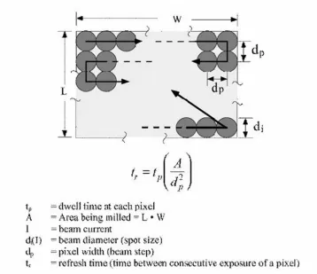
Refresh time is a function of the dwell time, the beam diameter and percent overlap (which together determine the number of pixels) and the size of the scan area. It is defined by the equation
2 )) 1 ( ( ) ( OL d w l p D R − + = τ
τ (12)
where l and w are the length and width of the scan area and OL is the beam overlap ranging from 0 (no overlap) to 1 (100 % overlap and the beam doesn’t move).
Figure 5. Schematic diagram showing the relationship between deposition efficiency and refresh time in arbitrary units. The maximum in deposition efficiency occurs when it is approximately equal to the monolayer formation time (based on model proposed by Koops61).
Figure 6. Diagram depicting the interdependent relationship between refresh time and box size, probe diameter, pixel overlap and dwell timeError! Bookmark not defined..
The amount of time required for one monolayer to adsorb is different for all precursor and substrate combinations depending on sticking coefficient, molecular size and mass, and molecular flux. The monolayer formation time is given by the equation63
2 2
2 1
o o
mono
d kT n
m Fd
t = = π (13)
where F is the molecular flux, m is the molecular mass [g/mole], n is the molecular density of the gas phase precursor [molecules/cm3] and do is the molecular size [nm2].
2.4.5 Proposed Models
The previous sections in this chapter have presented the fundamental physics of precursor introduction, precursor-substrate interactions, interactions of the beam with the adsorbed molecules and substrate and the effects of beam and scan parameters on
deposition rate and efficiency. The understanding of the process has been greatly elucidated by proposed models attempting to explain the mechanisms and gain insight into ways to maximize the reaction rate, increase resolution or enhance the purity of the depositions. In this section models proposed by Koops, Harriott and Hoffman will be briefly described and compared to one another.
Koops et al. proposed a model for the EB induced deposition process and used W(CO)6 and Me2Au(tfac) precursors with a silicon substrate to test their model. They used the Scheuer approach64 in which the adsorbed molecular density at the surface is given by qNf N N N gF dt dN o − − ⎟⎟ ⎠ ⎞ ⎜⎜ ⎝ ⎛ − = τ
1 (14)
where g is the sticking coefficient (0.5-1 is assumed), F is the molecular flux at the substrate (reasonable value is 1019 molecules/cm2s), No is the adsorption site density (typically 1015 sites/cm2), f is the electron flux (1018-1019 e-/cm2s) and q is the
dissociation cross section (10-15 cm2 at the maximum) for the adsorbed molecules under electron bombardment and τ is the residence time (around 0.1 s).
Harriott65 proposes a similar model for FIB gas assisted etching in which the precursor molecules reside on the surface until desorption or a chemical reaction caused by ion beam irradiation occurs. The adsorption rate is given by
o e o N N t msI N N N gF dt dN ) (
1 ⎟⎟− −
⎠ ⎞ ⎜⎜ ⎝ ⎛ − =
τ (15)
reacted surface atoms that can be removed by a single ion and depends on the surface binding energy of the reacted substrate atoms and the energy of the incoming beam.
The first term in equations 14 and 15 are identical and represent the adsorption of vapor phase molecules to the surface. This term depends on the molecular flux
impinging on the specimen surface, the sticking coefficient, and the number of available adsorption sites on the surface as monolayer adsorption is assumed. The second term in both equations is the desorption rate which is equal to the adsorbed molecule surface density divided by the residence time. Both models are the same to this point.
The final term represents the consumption of adsorbed molecules by deposition by Koops or etching by Harriott. In Koop’s model the consumption of molecules by deposition depends on the dissociation cross-section, the electron flux and number of adsorbed molecules. Harriott’s model describes the consumption of molecules from CE-FIB with the number of molecules required to remove a substrate atom, maximum etch yield of atoms per incident ion, ion beam flux and ratio of gas molecule density to adsorption site density. The negative indicates the molecules are being used up.
Previous sections addressed the fact that vapor phase adsorption is not the only supply mechanism. Surface diffusion is not taken into consideration in either of the 2 models discussed above but has been shown to be significant by many authors,,. There should therefore be another positive term alongside the vapor phase adsorption term indicating the resupply of precursor molecules by diffusion across the sample surface.
This issue was addressed by Hoffman et al.66 who modified the equation for electron beam induced deposition to accommodate for surface diffusion as follows
n D nf n n n sJ dt dn o o 2
1 ⎟⎟− − + ∇
⎠ ⎞ ⎜⎜ ⎝ ⎛ − = σ
τ (16)
The equation for deposition rate proposed by Hoffman is considered to be the most complete model and can be used for EB or FIB induced chemistry. By replacing the third term in equation 16 with that of the third term in equation 15 proposed by Harriott, the Hoffman model can be used to describe the FIB induced etching rate. These models help to theoretically visualize the fundamental physics of these processes.
2.5 Electron Beam Induced Chemistry
This section provides a thorough overview of electron beam induced chemistry. It begins with early literature on reducing beam induced contamination and continues on with its first applications to nanofabrication and its evolution into the current techniques using introduced precursors. Various different precursors and results are presented for both deposition and etching using electron beam induced chemistry.
2.5.1 Beam Induced Contamination
Beam-induced contamination has been studied since Stewart described the
formation of insulating films inside vacuum tubes due to electron and ion beam exposure in 193467. Contamination is a general term used to describe the accumulation of foreign material on the surface of a sample due to electron or ion beam irradiation68. This build-up generally results in a thin contamination blanket over the scanned area or a vertical pillar in the case of a stationary beam, leading to a loss in imaging resolution and change in specimen topography and surface composition. Electron microscopy imaging at magnifications above 50,000x is significantly affected and observations of surface modification have been reported at 20,000x in some systems58. Electron lithography techniques utilizing a precursor are very sensitive as contamination buildup can interfere with etch processes or degrade the composition of deposited materials97,91.
interactions near exposed areas excite and rupture common –CH, -COOH, -CNH2, and other bonds, resulting in the release of non-volatile molecules and the formation of carbon double bonds70. This cross-linking is responsible for the accumulation of amorphous carbonaceous deposits.
Hydrocarbon presence in the vacuum chamber arises from several sources including the sample itself, desorption from previously loaded samples, backstreaming from oil pumps and outgassing from 0-rings and stage lubricants. Hydrocarbon molecules are present on the surface of the sample before it is inserted into the SEM and hence the specimen acts as its own source. These molecules adsorb to the sample surface “during the specimen preparation procedure or during storage or transfer through the normal air”71 and remain on the surface upon insertion. Once inside the chamber the molecules randomly migrate along the surface or desorb into the chamber of the SEM where they remain in the gas phase or adsorb to chamber sidewalls and components.
Backstreaming of oils72,73 can introduce hydrocarbons to the sample from rotary vacuum pumps or from oil filled diffusion pump systems used to evacuate the main chamber or sample introduction chamber74. Molecular sieves or cold traps can be employed to reduce backstreaming, but it is impossible to completely eliminate all hydrocarbons introduced by backstreaming without using an oil-free pumping system.
XEI Scientific75 has developed a commercial system that is externally mounted on the vacuum chamber of a SEM in order to actively remove hydrocarbon
contamination from the chamber. The Evactron RF plasma cleaner uses air to produce oxygen radicals to chemically remove oils and hydrocarbons from the inside of the chamber.
Ellis proposes that the contamination electron microscopes is due to the polymerization of hydrocarbons migrating along the surface from chamber walls76. Egerton’s71 observations indicate that the source of the hydrocarbon contamination is indeed surface diffusion across the specimen. Surface migration is also supported by the work of Amman who deposited contamination lines of different length in order to vary the time for the beam to return to the same point (delay or refresh time)77. Significant contamination occurs for large delay times but for short delay times there is insufficient time for hydrocarbons to resupply the exposed region. Hren has shown that a focused beam of 1 μm results in a ring of deposition instead of a cylinder because the adsorbed hydrocarbons “on the specimen diffuse along its surface towards the edge of the irradiated area and are immobilized there”78.
There are arguments for each case but it is most probable that the vapor adsorption and surface diffusion supply mechanisms are both present and that the contributions vary for different precursor-substrate systems. Additional, controlled experiments are needed, including temperature dependent studies in order to further our understanding of the process.
Among the first applications was the use of contamination deposits to study astigmatism in the beams of probe forming systems in 195679. Contamination writing has been considered for use as a form of lithography as proposed by Broers in 196480 because the carbonaceous deposits are resistant to subsequent anisotropic ion etching. In 1976 Broers was successful in using contamination writing to deposit a carbon mask on 10 nm thick gold palladium film81. The film was then ion etched resulting in feature linewidths of less than 80 Å. Electron beam written patterns using contamination have been used as masks for pattern transfer82.
imaging performance on both soft (PMMA) and hard (diamond) surfaces. Free-standing carbon nanoelectrodes have been successfully fabricated with a gap of less than 5 nm suitable to study electrical transport properties of molecules and nanoclusters88. Deposition of contamination has also been used for the fabrication of nanotweezers for use in the AFM89.
Contamination buildup has been seen as an issue since the early days of electron microscopy causing changes in specimen topography and a reduction in resolution. As EBID techniques were developed, the incorporation of impurities due to hydrocarbon presence contaminated the purity of the resulting deposits altering their material
properties. Contamination has however been utilized as a mask and for nanofabrication of various tools and structures. It is important to understand the contamination
mechanisms in order to reduce it for electron microscopy or to maximize it for use as a precursor.
2.5.2 Electron Beam Induced Deposition
Several research groups have pursued experimentation and modeling of EB induced deposition in the last few decades and their works are presented in this section. Research efforts are usually focused on obtaining a high deposition rate, high resolution and/or high purity of the deposited material in order to obtain desirable material
properties.
For EB induced deposition to occur a precursor is selected that has a sufficient sticking coefficient (close to 1) and reasonable residence time (0.1-1 s) on the substrate. Both of these increase the probability that sufficient precursor molecules are present at every pixel for the maximum deposition efficiency to be obtained. The molecules must rapidly decompose under electron beam irradiation into a volatile portion which is pumped away, and a non-volatile fragment which remains on the sample in the form of a deposit with the desired properties. Volatile by-products should have a short residence time (less than the refresh time) in order to prevent incorporation into the deposit thus reducing the purity.