Design and Simulation of a Low-Voltage Low-Offset Amplifier
Abhimanu Surendra K Singh & Poonam Pathak
#
Electronics & Communication, R.G.P.V Bhopal L.K.C.T. Indore M.P. India
1
[email protected]
2
[email protected]
Abstract
—
In many applications, offset of the OP-AMPs should be cancelled to high accuracy be accomplished. In this work, an asymmetrical differential input circuit with active DC offset rejection circuit was implemented to minimize the systematic offset of the amplifier. The proposed OP-AMPs show that the systematic offset voltages is less than 80μV.Keywords—component; formatting; style; styling; insert
Introduction
The CMOS Op-Amp is an important building block of
linear and switched-capacitor circuits. However,
mismatch of the devices causes an offset voltage, which
limits the high-precision application. Commonly, the
offset sources of OP-AMPs are categorized as systematic
offset and random offset. The systematic offset happens
because of the channel length modulation of transistors
and the value of the offset voltages are the functions of
the input and output common mode voltages [1, 2, 3].
For example, in the formal OP-AMPs, the channel length
modulation of transistor shows the systematic offset.
However, the channel length modulation is unimportant,
with no feedback, the output common mode voltage ever
shows the fixed voltage level and doesn’t follow the
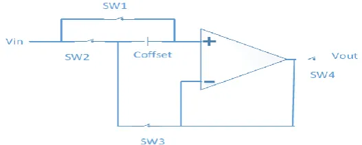
The general method of offset cancelation of OP-AMPs is
the feedback-capacitor circuit as shown in Fig.1 [7]. At
first, as the switch 1 and 2 are turned on, the offset
voltage is stored in C offset. Then the offset of VOUT is
omitted when the switch 1 and 2 are turned off and the
switch 3 and 4 are turned on. But this circuit has some
disadvantages of large capacitor, and many CMOS
switches which is the source of the switching error. In
this work, a continuous time asymmetrical differential
input circuit with common mode feedback circuit which
can minimize the offset of OP-AMPs is presented.
Fig. 1. Typical Offset Compensation Circuit
II. CIRCUIT DESCRIPTION
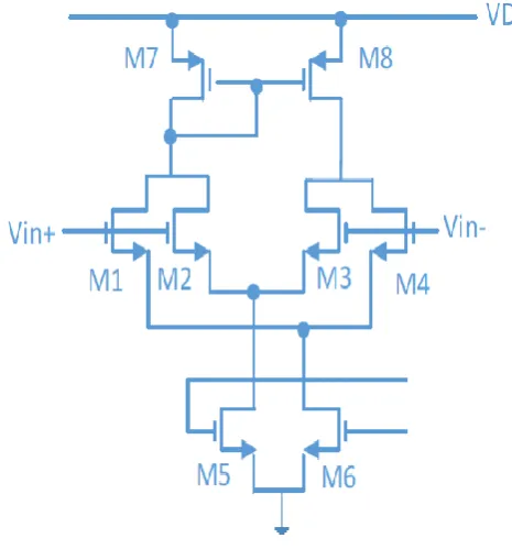
The proposed OP-AMP is composed of three parts:
M9-M12 and current sources M14-M17 [10, 8].
Fig. 2. Input Stage
The second stage is the combination of M
14-M19. Long
channel NMOS transistors are used for input stage to
minimize the differential pair nonlinearity and to insert
more input voltage swing. They also minimize the V
bias
9 12
common-mode level of the input and the output could be
detected and amplified by the DC offset rejection circuit,
and changed to the feedback signal for current sinks of
the amplifier. This is a negative feedback network.
By adjusting the current of the current sinks, the input
and the output common-mode voltage would be
maintained in same level to minimize the systematic
offset. The difference between input and output
common-mode level will be amplified. In the proposed
circuit, the sum of drain currents, I
M5 and IM6 is constant.
Therefore, small signal differential mode open loop
voltage gain of input stage is given by:
Avd,input-stage = -(gm(M3) +gm(M4)).(ro(M8) II
ro(M3) II ro(M4) )
Where gm is the transconductance and ro is the output
resistance of transistor. The total small signal open loop
differential mode voltage gains are given by:
Avd = (Avd,CMFB-stage). (Avd,input-stage).
Fig. 3. DC Offset Rejection Circuit
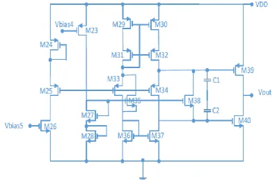
III. OUTPUT STAGE
The class-AB output stage shown in Figure 4, is
composed of an output buffer. Transistor M
23-M26 form two
floating current sources to provide bias current of
branches, which confirm the transistor M
33, M34, M35 and
M
36 work in saturation region. Their gate voltages are
provided by two biasing branches respectively. The
current signal I
IN1 and IIN2 are subtracted through current
mirror and amplified by push-pull stage [10, 2].
Fig. 4. Output Circuit
IV. SIMULATION CIRCUIT
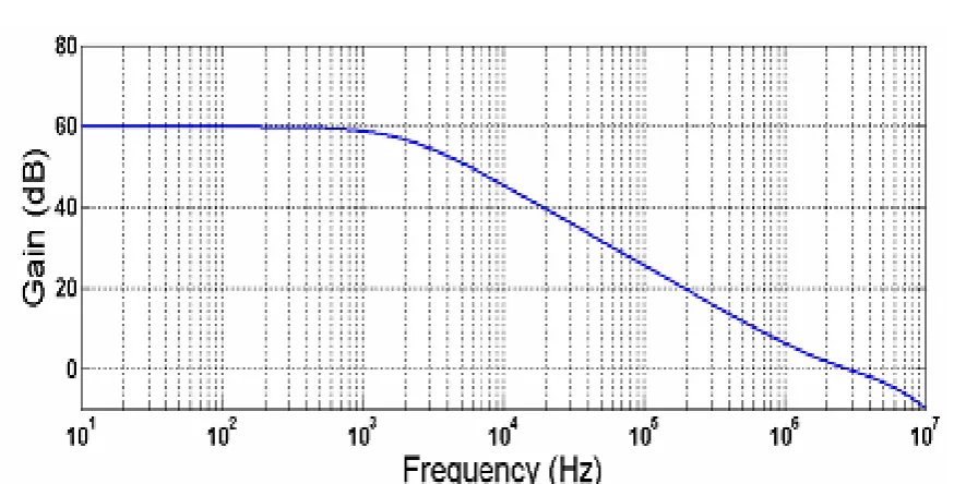
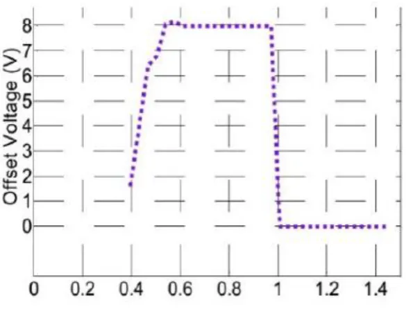
Figure 5 shows the AC responses of the proposed OP-AMP
while driving a 2 pF load. It shows 60 dB open-loop gain,
63.5° phase margin, and 2.82 MHz unity gain bandwidth.
DC sweep analysis of the amplifier connected in an
inverting unity-gain configuration is shown in figure 6. The
simulation results showed good following characteristic
between Vin and Vout , and the offset voltage less than 80
Input Offset Voltage 80μV
V. CONCLUSION
An offset cancellation technique that uses an asymmetrical
differential input circuit with active DC offset rejection
circuit has been presented. Simulation results show that
Op-Amp offset voltage is less than 80μV in entire
operating voltage range.
REFERENCES
[1] B. Razavi, Design of Analog CMOS Integrated Circuits,
McGraw-Hill, 2002, pp.291-336.
[2] D. A. Johns and K. Martin, Analog Integrated Circuit
Design, New York: John Wiley & Sons, Inc., 1997,
pp.221-251.
[3] J. H. Huijsing, R. Hogervorst and K. J. de Langen, “Low power low voltage VLSI operational amplifiers cells”,
IEEE Transactions on Circuits and Systems I, vol. 42,
pp.841-852, Nov. 1995.
[4] J. Y. Zhang, L. Wang and B. Li, “Design of Low Offset
Low Power CMOS Amplifier for Biosensor
Application”, J Biomed Sci Eng, vol. 2, pp.538-542,
2009.
[5] K. T. Lim, S. J. Kim and O. K. Kwon, “The
OP-Amplifier with offset cancelation circuit”, IEEE,
pp.445-447, 2003.
[6] P. E Allen and D. R Holberg, CMOS Analog Circuit
Design, Second Edition, New York, Oxford University
Press Inc., 2002, pp.352-415.
[7] P. Kakoty, “Design of a high frequency low voltage CMOS operational amplifier”, Int. j. VLSI des.
commun. Syst, vol. 2, pp.3680-3692, March 2011.
[8] R. Jacob Baker, CMOS Circuit Design, Layout and
[9] S. Franco, Design with Operational Amplifiers and
Analog Integrated Circuits, McGraw-Hill College, 1988,
pp.60-92.
[10] S. Sheikhaei, S. Mirabbasi, and A. Ivanov, “A 0.35m
CMOS Comparator Circuit For High-Speed ADC
Applications”, IEEE, vol. 6, pp.6134 - 6137,2005.
[11] Y. Tsividis, Operation and Modeling of the MOS
Transistor, 2nd ed, Boston, MA: McGraw-Hill, 1998,