Integrated Power Converter for Distributed
Generation
D.Dastagiri, C.Ravi varma
PG Student [EPS], Dept. of EEE, Sree Vidyanikethan Engineering College, Tirupati, A.P, India
Assistant Professor, Dept. of EEE, Sree Vidyanikethan Engineering College, Tirupati, A.P, India
ABSTRACT: Distributed generation systems with the using of the renewable sources increasingly, application of the distributed generation (DG) in the distribution system acquired more attention. After the power system faults, distribution system which contains many DGs would usually cut off the DGs from the distribution system at the joint where the DGs connected into the system term less. However, considering the enlarge scale and the capability of the DGs, also with the improving ratio of the DG to all generator, cut off the DGs from the distribution system directly without analysis of the splitting point detailed after the faults occurs in the power system, which cannot improve the reliability of the distribution system and made the effect of the DG at a discount. Distributed generation systems also include local energy sources, storages, and loads. Almost always, these entities have their own power converters for grid interfacing and energy processing. Having individual converters has advantages like more flexible individual control and simpler design but does not encourage functionality merging. Reduction of semiconductors to arrive at a more compact integrated design is thus not possible. Addressing this concern, a number of integrated energy generation systems that use 25% lesser semiconductors are proposed. The systems can be single or three phase depending on the types of sources, storages, and loads assembled. They can operate in the grid-tied or stand-alone mode with no compromise in performances expected, when compared with other solutions using more switches.
KEYWORDS: Distributed generation (DG), energy storages, energy systems, microgrids, pulse width-modulated converters.
I. INTRODUCTION
perform some integration rather than use multiple individual converters as per existing practice. For that, a number of integrated energy systems using 25% lesser semiconductors are proposed here for DG [1]. Operating principles and advantages of the systems proposed are first clarified before considering their likely performance tradeoffs. These tradeoffs cannot be avoided by most (if not all) reduced semiconductor topologies but can surely be minimized for the systems proposed. Relevant explanation can be found in a later section, together with experimental results for proving the practicalities of the systems proposed.
II. ENERGY GENERATION SYSTEMS WITH NON INTEGRATED POWER CONVERTERS
Fig.1.1 (a) shows the typical block representation of a common solar energy generation system drawn here for example. Each source or storage included is accompanied by its own dc–dc boost or charging converter tied to a common dc link. The harnessed energy is then forwarded to a dc–ac inverter for conditioning before channeling it to the grid. The inverter can either be single or three phase, even though the latter is explicitly drawn in the diagram. It is also not necessary for the dc–ac inverter to tie to the grid if the energy generated is meant for immediate load consumption in an islanded local microgrid. The dc–ac inverter in an islanded microgrid can also be replaced by a dc–dc converter if the loads are dc by nature. DC network is certainly a possibility, but based on present advancement, ac output would probably continue to dominate for many more
Fig.1.1. Example (a) block diagram and (b) circuit layout of nonintegrated energy system.
the indicated solar panel in Fig.1.1 (b) is replaced by another type of source that can absorb backward flow of energy. Regardless of that, the system shown in Fig.1.1 (b) clearly lacks integration. Its formation is simply by connecting individual well-known converters to a common dc link. The system is thus fully decoupled with each converter having virtually no influence on the others. Surely, this is an advantage, but because of the intermittent nature of the solar source (in fact, most renewable sources) and battery charging process, most of the converters would likely not operate continuously at their rated capacities[2]. The resulting system built with multiple individual converters is hence neither cost effective nor compact. The suggestion is then to introduce some amount of integration to the system to cut down on its number of semiconductors. The integrated system must produce comparable input and output performances as the fully decoupled system. Like all reduced semiconductor topologies though, some tradeoffs like higher voltage stresses and control limitations would likely surface.but can surely be minimized if designed appropriately. Approaches to realize the minimization for the proposed single- and three-phase energy systems are now described as follows.
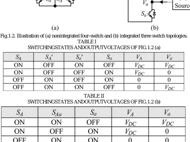
Fig.1.2. Illustration of (a) nonintegrated four-switch and (b) integrated three switch topologies. TABLE I
SWITCHINGSTATES ANDOUTPUTVOLTAGES OF FIG.1.2 (a)
TABLE II
III. INTEGRATEDENERGYGENERATIONSYSTEMS
A. Method of Integration
The integration principles are better explained by referring first to the nonintegrated energy system shown in Fig.1.1 (b). For easier viewing, two of its phase legs with switches {SA,S’A , Sa, S’a} are drawn separately, as shown in Fig.1.2 (a). For each of the illustrated phase legs, its two switches must be switched in complement, meaning that, when one switch is on, the other must be off. Terminal voltage of the considered phase leg can then produce two discrete values identified as Vdc and 0 V. The same applies to the other phase leg shown in Fig.1.2 (a). Terminal voltages of the two phase legs can then be any of the four sets of values indicated in Table I. Instead of two independent phase legs, the switches can be rearranged as shown in Fig.1.2 (b) while still providing two terminal voltages. Instead of four switches, only three switches labeled as {SA, SAa, Sa} are used. That represents a saving of 25%, which can be sizable if more switches are considered. Among the three switches, two of them will be turned on to tie the terminal voltages to either the same or different dc rails at any instant. The three possibilities are summarized in Table II, which, when compared with Table I, tells a constraint faced by the three-switch topology. To be more precise, the terminal voltages of the three-switch topology cannot produce the fourth combination of VA = 0V and Va = Vdc, which certainly is a tradeoff incurred by saving one switch. The overall system design should therefore be planned such that influences from this tradeoff on the terminal voltages
Fig.1.3 Integrated three-phase energy system with multiple sources and storages.
B. Modulation Principles
Referring again to those two simplified illustrations shown in Fig.1.2, making them produce the same terminal voltages
Fig.1.4. Carrier band division and gating signal generation per phase leg.
would demand that they share the same modulation theories. Some constraints would however be accompanying the three switch topology shown in Fig.1.2 (b) since it uses lesser switches. A convenient way of explaining the three-switch modulation is hence to focus on the more established independent phase legs shown in Fig.1.2 (a) first, before shifting the knowledge with constraints added to Fig.1.2 (b). With the circuit shown in Fig.1.2 (a), the phase leg tied to the dc source is, in theory, controlled by a dc reference and a triangular or saw-tooth carrier. The second phase leg tied to a phase of the three-phase ac grid is similarly controlled by a sinusoidal reference and a triangular carrier (saw-tooth carrier not considered here since it has no spectral benefit). Strictly, carriers of the two phase legs need not be the same, but in practice, using one carrier has the benefit of involving only one timer. It is hence advisable to use a common carrier and two independent references for the circuit shown in Fig.1.2 (a). The same independence cannot be introduced to the integrated topology shown in Fig.1.2 (b), whose sinusoidal reference for the upper terminal must always be placed above its linear reference for the lower terminal. Such placement helps to avoid the fourth restricted state of VA = 0V and Va = Vdc. An example illustrating the three-switch modulation is shown in Fig.1.4, where a single carrier band is clearly divided into h1 and h2. The upper sub band h1is assigned to the upper terminal and hence confines the sinusoidal reference. Similarly, the lower sub band h2 is assigned to the lower terminal and hence encompasses the linear reference. Comparing the references with the single common carrier based on the following rules then leads to those gating signals for SA and Sa shown at the bottom of Fig.1.4
(1.1)
To ensure that only two switches are on and hence produce any of the three combinations shown in Table II, the gating signal for the middle switch SAa must be derived from the earlier two based on the following:
Fig.1.5. Other integrated configurations for (a) three- and (b) single-phase grid-tied energy conversions.
Where ⊕ is the logical XOR operator and !SA and !Sa are the complements of SA and Sa with dead time added. Operating on !SA and Sa is recommended since it automatically creates the dead time needed by SAa to avoid shorting the three switches simultaneously . The full set of gating signals obtained (e.g., bottom of Fig.1.4) is thus always in agreement with the allowed states summarized in Table II. Another concern noted with the modulation process is the dc offset added to the sinusoidal reference for centering it within h1.Like triplen, this offset is added to all phases of a three phase system and will therefore be cancelled in the line-to-line voltages.
C. Parameters and Constraints
As mentioned earlier, the lower subbandh2 in Fig.1.4 is assigned to the lower terminal of the three-switch topology shown in Fig.1.2 (b). Given that it is tied to a dc source, the usual parameter of interest would be the duty ratio d or fractional on time of the lower switch Sa. The range of variation of d and its accompanied gain Gdc (= 1/(1−d))can accordingly be determined as
(1.3)
the three-switch topology shown in Fig.1.2 (b), since it is tied to an ac source, its parameter of interest would be the modulation index M. Referring to Fig.1.4, M represents the amplitude of the sinusoidal reference, which, in theory, is also equal to the resulting buck gain Gac. Its value can vary within the range spelled in (1.4), where the factor of 1.15 is added for representing triplen insertion.
(1.4)
The value of M is also known to vary inversely with the dc-link voltage Vdc (M∝1/Vdc)in the case of a fixed ac grid voltage. Lowering Vdc therefore requires M and, hence, h1to be high. That means h2 = 2 − h1in Fig.1.4 must be low, which, for the proposed energy system, is fine since a high dc gain Gdc is needed, as explained earlier. The proposed energy system is therefore a more suitable system for applying the three-switch topology shown in Fig.1.2 (b) rather than those ac–ac converters. In those references, Vdc is doubled because M is set to a maximum of only 0.5.
D. Other Integrated Configurations
Instead of the system shown in Fig.1.3, the three-switch topology shown in Fig.1.2 (b) can be used to form other energy systems. Two proposed examples are shown in Fig.1.5 (a) and (b), where, again, three three-switch phase legs are shown. In general, the number of three-switch phase legs connected in parallel can be any positive integer
Fig.1.6. Illustration of dc-link voltage increase for three-switch topology.
number. It depends on the number of sources, storages, and loads connected together. Where needed, traditional two-switch phase legs can also be added in parallel to the three-switch phase legs. This extension is relatively straightforward and will hence not be explicitly shown in this paper. Rather, the intention for including Fig.1.5 (a) is to show the additional possibility of connecting a solar panel (indicated only as an example) to the dc link through its dc–dc converter. Unlike Fig.1.3, no source is now connected to the lower three dc terminals, which are instead tied to three storages (two batteries and an ultracapacitor). The system however retains its three-phase ac grid interfacing like in Fig.1.3. For illustrating single-phase grid interfacing, Fig.1.5 (b) is referred to instead, where two of its upper terminals are used for single-phase grid interfacing. The same dc offset as in Fig.1.4 must still be added to the two 180◦
phase-shifted sinusoidal references for the two upper terminals, which, when subtracted, will not appear in the ac voltage (VA−VB). Since the third upper terminal is now not used for grid interfacing, it can either be removed together with switch SC or tied to a dc load, as shown in Fig.1.5 (b). Other connections to the lower three dc terminals in Fig.1.5 (b) remain unchanged as in Fig.1.3.
IV. THREE-SWITCH VERSUS FOUR-SWITCH TOPOLOGY
A. Dc-link voltage
dc-link voltage Vdc of the three-switch topology is thus computed as (3.48/h1) p.u. for the three-phase systems shown in Figs.1.3 and 1.5 (a). [As mentioned earlier, a multiplication factor of 1.15 needs to be included for the single-phase system shown in Fig.1.5 (b).] In percentage term, it represents an increase given by
(1.5)
TABLE III
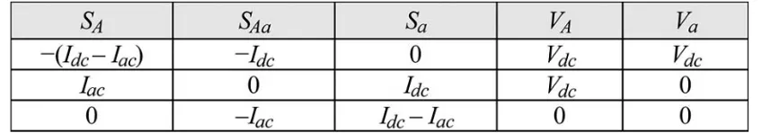
Currents through Switches at different Output Voltages for Four-Switch Topology
Variation of (1.5) is shown in Fig.1.6, from which it is read that the increase is 100% or doubled when h1=1 or M= 0.5. This doubling of dc-link voltage is experienced by those ac–ac converters , which conceptually can be reduced here by increasingh1. For example, if h1 is raised to 1.6 and 1.8, the increase ΔVdc would be 25% and 11%, respectively. It is hence important to keep one sub band much wider than the other (h1 h2 shown in Fig.1.4), which, fortunately, is a requirement enforced by the proposed energy systems. This identification has so far not been discussed in the open literature. When dividing the carrier band, it is also of concern to mention here that the upper subbandh1must include all upper references and the lower sub band h2 must include all lower references. That indirectly means that the highest modulating references in both sub bands will decide on the appropriate level to divide in the full carrier band. These references correspond to the highest upper and lower terminal voltages that the inverter can manage.
B. Switch Currents and Overall System Losses
TABLE I V
Currents through switches at different output voltages for three-switch topology
The currents obtained in Tables III (first three rows only) and IV can then be compared for each pair of terminal voltages produced. The conclusions drawn are summarized hereinafter.
1) By eliminating one switch, the middle switch SAa of the three-switch topology carries the same current as either S’A or S’a of the four-switch topology, depending on the state presently being assumed.
2) The current through SA of the three-switch topology has an interval over which its current is − (Idc− Iac). Otherwise, it is closely similar to the current flowing through SA of the four-switch topology.
3) The current through Sa of the three-switch topology is similar to that flowing through the same switch of the four-switch topology, except for an interval over which the current is (Idc−Iac). It should be noted here that the absolute amplitude of the current (Idc−Iac) depends on the amount of boosting introduced and the individual current polarities (e.g., charging or discharging, terminals connected to sources, storages, or loads). Instantaneous current stresses might therefore be raised, but that does not imply the same for the overall system losses. On average, if a good mix of different entities is tied to the integrated system, its losses should be either comparable or slightly raised as compared to its nonintegrated counterpart. The slightly higher losses are mainly caused by the slightly higher dc-link voltage needed by the integrated system, as understood from Fig.1.4.
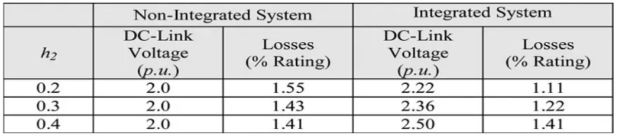
To demonstrate, the overall losses of the nonintegrated and integrated energy systems shown in Figs.1.1 (b) and 1.3 have been computed based on the simulation approach. Switches used for the simulation are 600-V/50-A insulated gate bipolar transistors (IGBTs), whose parameters can be found. For both systems, energy flow has been tuned to flow from the solar source to the ac grid and storages. Results obtained are tabulated in Table V for small lh2≤0.4, which is in
accordance to the earlier suggested band sizing requirement. The results show that, for smaller h2, losses of the nonintegrated energy system increase because of the lower dc terminal voltages and hence higher dc terminal currents if the system power is kept constant. The integrated system, on the other hand, has its losses reduced because of the lower dc-link voltage associated with a smaller h2. This trend is applicable to both three-phase systems shown in Figs.1.3 and 1.5(a), except for higher loss values anticipated with Fig.1.5(a) because of its additional switch S, diode D, and other passive components. The evaluation is next performed with the three-phase grid in Fig.1.1 (b) replaced by a single-phase grid and a resistive load like those shown in Fig.1.5 (b) for the single-phase integrated system. Results obtained for both systems can be found in Table VI, which, upon compared, show lower losses for the integrated
TABLE V
TABLE VI
Losses of energy systems with single-phase grid
system. The reason might probably be linked to the third upper terminal supplying a positive current to the dc load. The earlier notated upper current Iac is thus always positive, which, when subtracted from Idc, will always lead to a smaller (Idc−Iac) for the third three-switch phase leg. Since its currents are reduced, its losses will reduce accordingly too.
V. CONTROLPRINCIPLES
In this section, only the control schemes for the integrated energy system shown in Fig.1.3 are explained in detail. This does not compromise generality since the other two discussed systems in Fig.1.5 (a) and (b) and the nonintegrated system shown in Fig.1.1 (b) share the same control principles. The same control schemes were, in fact, used for single- and three phase experimental testing, whose results are shown in a later section. It is hence appropriate to consider only Fig.1.3 with its upper dc–ac inverter control discussed now with reference to the upper half of Fig.1.7. In that representation, the dc link voltage Vdc is first measured, before being regulated by a classical proportional (P)-integral (I) (PI) controller to follow a defined command V*dc. Parameters of this PI controller are designed based on, where the inner current loop, being much faster, is replaced by a time lap and a low-pass-filter block for representing computational delay and capacitor charging dynamics. The P and I gains are then chosen as K=0.1 and Ki1=10 to give enough phase margin for maintaining the overall system stability. The PI output, being the active current amplitude needed for keeping Vdc constant, is then multiplied with a unit sine synchronized with the ac grid voltage V grid by a standard phase locked loop. The resulting ac signal I*ac represents the in-phase active current reference fed to the inner current loop. The inner current controller can no longer be a PI controller, whose steady-state error is not zero because of its finite gain at the ac frequency of interest. A P–resonant (PR) controller is used instead, whose transfer expression is written as
Fig.1.7. Per-phase illustration of the overall control schemes.
Fig.1.8. Per-phase ac inner current loop.
Where Kp2 and Ki2 are the controller gains and ωc and ωo are the angular cutoff and fundamental frequencies, respectively. Bode diagrams of (1.6) will, in theory, have a high resonant peak at the 50-Hz frequency of interest. This
peak will gradually tend toward infinity as ωc→0. The final tracking performance of the inner current loop can be verified by referring to its control block diagram drawn separately in Fig.1.8. Filter impedance (R+sL) and grid voltage V grid have now been included in the figure for arriving at its closed-loop transfer function written in (1.7). The derived transfer function clearly has two terms for informing that, if the controller gains are chosen high enough, Iac will follow its reference I*ac exactly with little influence from V grid
(1.7)
Fig.1.9. Bode plots of feedforward path of Fig.1.8.
margin at the system crossover frequency (instant at which magnitude response drops to 0 dB). The system is thus stable. The second step is to design the resonant gain so that acceptably small steady-state errors are produced, together with a satisfactory phase margin. The chosen resonant gain here is Ki2 = 10, which will alter only the magnitude response around 50 Hz and not at the crossover frequency. The final phase margin is thus still more than 60◦, which, needless to say, represents a stable system. Cutoff frequency ωc can next be chosen, whose purpose is mainly to lessen selectiveness by Fig.1. 9. Bode plots of feed forward path of Fig.1. 8. widening the bandwidth around the resonant peak. This can be helpful if the 50-Hz resonance frequency varies slightly but should not be excessive since the resonant peak amplitude drops significantly as ωc increases. The resulting signal from the properly designed PR controller then forms the required ac modulating reference (upper sinusoidal reference in Fig.1. 4) needed for switching pulse generation. For that, a timer counting from zero to one and then back is used for realizing a positively displaced triangular carrier, unlike that shown in Fig.1. 4. The ac modulating reference should therefore be changed according to (1.8), whose effect is still to place the reference centrally within the upper subband h1
V_ac_PWM = 0.5Vac_PWMh1 + 1
−
0.5h1. ………
(1.8)Fig.1. 10. Experimental setups and parameters used for (a) single- and (b) three-phase energy systems.
Fig.1. 11. Modulating references for single-phase system in Fig. 10(a) and three-phase system in Fig. 10(b) before transient. (a) Single phase. (b) Three phase.
earlier, no dc offset needs to be added to Mdc, unlike the ac reference Vac_PWM. In general, the presented control schemes function well with the same steady-state responses produced by the nonintegrated and integrated energy systems, if controlled by the same control schemes. Their transient responses are however different caused by coupling introduced by the integrated energy system. To illustrate, a transient step decrease in dc source current
VI. EXPERIMENTALRESULTS
For verification of practicality, scaled-down prototypes shown in Fig.1.10(a) and (b) were assembled in the laboratory using the parameters indicated in the figures (values chosen from those available in the laboratory and, hence, not optimized). Fig.1.10(a) was clearly a single-phase grid-tied system with two of its upper terminals connected to one phase of a 155-V (line-to-line rms) 50-Hz three-phase ac grid and a local single-phase ac load of 30 Ω. The third upper terminal was tied to a local dc load of 13 Ω, while the lower three terminals were connected to three separate dc sources
of 30 V each. Two 180◦phase-shifted sinusoidal and four linear references were thus needed, as shown in Fig. 1.11(a). In the figure, two upper sinusoidal references and a single linear load reference
at Mdc = 0.33 were shown occupying the upper subband with a width of h1/2 = 0.8. Also shown in the figure were three lower linear references clustering around Mdc = 0.15 for the dc sources. They occupy the lower narrower subband with a width of h2/2 = 0.2.
Fig.1.12. Experimental waveforms of single-phase system in Fig.1.10(a). (a) Transient 1. (b) Transient 2.
with the local dc load demand kept unchanged. Power output from dc source 1 therefore dropped to zero in the fourth trace, while the dc load current in the last trace remained constant. The amount of surplus energy injected to the grid was thus reduced, causing the ac supply current in the second plot of Fig.1.12(a) to drop. The same initial conditions in Fig.1.12(a) were repeated in Fig.1. 12(b), whose transient event at t = 100 ms was triggered by turning off dc sources 1 and 2 with the dc load demand kept unchanged. Power values in the fourth and fifth traces of Fig.1.12(b) therefore dropped to zero with the load current in the last trace kept constant. The remaining dc source 3 was not able to power the load fully, hence causing the ac grid current in the second trace to reverse. The ac grid current was now in phase with the ac grid voltage, representing energy drawn from the grid. Testing was next performed on the three-phase system shown in Fig.1.10(b) with its upper three terminals tied to the three phase ac grid and a local ac load of 20 Ω per phase. The
lower three terminals were connected to two 50-V dc sources and a 7-Ω dc load, respectively. The references needed were
therefore three upper sinusoidal references with triplen offset added and three lower linear references, occupying subbands h1 and h2 in Fig.1.11(b). The common dc-link voltage produced was 350 V, as seen from the third trace in Fig.1.13. This value could be reduced further by narrowing h2 or widening h1, as shown in Fig.1.6. Two transient events were also emulated here with the first shown in Fig.1.13(a). Throughout the illustrated duration, both dc sources were producing positive powers,
Fig.1.13. Experimental waveforms of three-phase system in Fig. 10(b). (a) Transient 1. (b) Transient 2.
These results clearly prove the effectiveness of the proposed integrated energy systems, which, in principle, can also be produced by the nonintegrated energy systems like the example shown in Fig. 1.1 (b). The integrated systems however have the following anticipated features, which have now been proven experimentally.
1) The same integrated configuration can be used for single and three-phase energy systems. 2) Doubling of dc-link voltage is not necessary, unlike those of ac–ac converters.
3) No significant deterioration of transient responses when applied to energy systems.
4) Energy flows through all terminals are not impeded by the converter merging, hence giving rise to no damaging surge or dip in voltage across the dc link. The dc-link voltage, in fact, remains nearly constant throughout the experiments. 5) Same implementation complexity with only one timer/ carrier and some dc offsets needed. DC offsets are usually added together with the triplens. Virtually the same performance is achieved with 25% lesser semiconductor.
VII. CONCLUSION
This project has proposed a number of integrated energy systems based on a compact converter topology. Through proper design, the proposed systems are shown to output equally good terminal waveform quality while yet gaining advantages like reduced switch count and compactness. Surely, some tradeoffs cannot be avoided but can be minimized through proper modulation planning and, hence, do not constitute a major problem. Experimental testing has already confirmed their conceptual validity and practicality, regardless of whether implemented in single- or three-phase form.
REFERENCES
[1] Poh Chiang Loh, Lei Zhang, and Feng Gao, “Compact Integrated Energy Systems for Distributed Generation,” ,” IEEE Trans. Ind.
Electron., vol. 60, no. 4, pp. 1137–1145, Apr. 2013.
[2] S. Vazquez, S. M. Lukic, E. Galvan, L. G. Franquelo, and J. M. Carrasco, “Energy storage systems for transport and grid applications,” IEEE
Trans. Ind. Electron., vol. 57, no. 12, pp. 3881– 3895, Dec. 2010.
[3] J. M. Carrasco, L. G. Franquelo, J. T. Bialasiewicz, E. Galvan, R. C. P. Guisado, M. A. M. Prats, J. I. Leon, and N. Moreno-Alfonso, “Power electronic systems for the grid integration of renewable energy sources : A survey,” IEEE Trans. Ind. Electron., vol. 53, no. 4, pp. 1002–1016,Jun. 2006.
[4] D. G. Holmes and T. A. Lipo, Pulse Width Modulation for Power Converters: Principles and Practice. Piscataway, NJ: Wiley, 2003. [5] Ned mohan, torem underland and william P. Robbins, Power Electronics Converters, Applications and Design, Third Edition,2000.